EP2200152B1 - Système photovoltaïque - Google Patents
Système photovoltaïque Download PDFInfo
- Publication number
- EP2200152B1 EP2200152B1 EP20080172418 EP08172418A EP2200152B1 EP 2200152 B1 EP2200152 B1 EP 2200152B1 EP 20080172418 EP20080172418 EP 20080172418 EP 08172418 A EP08172418 A EP 08172418A EP 2200152 B1 EP2200152 B1 EP 2200152B1
- Authority
- EP
- European Patent Office
- Prior art keywords
- voltage
- source
- photovoltaic
- route
- photovoltaic system
- Prior art date
- Legal status (The legal status is an assumption and is not a legal conclusion. Google has not performed a legal analysis and makes no representation as to the accuracy of the status listed.)
- Not-in-force
Links
Images


Classifications
-
- H—ELECTRICITY
- H02—GENERATION; CONVERSION OR DISTRIBUTION OF ELECTRIC POWER
- H02J—ELECTRIC POWER NETWORKS; CIRCUIT ARRANGEMENTS OR SYSTEMS FOR SUPPLYING OR DISTRIBUTING ELECTRIC POWER; SYSTEMS FOR STORING ELECTRIC ENERGY
- H02J7/00—Circuit arrangements for charging or discharging batteries or for supplying loads from batteries
- H02J7/34—Parallel operation in networks using both storage and other DC sources, e.g. providing buffering
- H02J7/35—Parallel operation in networks using both storage and other DC sources, e.g. providing buffering with light sensitive cells
-
- Y—GENERAL TAGGING OF NEW TECHNOLOGICAL DEVELOPMENTS; GENERAL TAGGING OF CROSS-SECTIONAL TECHNOLOGIES SPANNING OVER SEVERAL SECTIONS OF THE IPC; TECHNICAL SUBJECTS COVERED BY FORMER USPC CROSS-REFERENCE ART COLLECTIONS [XRACs] AND DIGESTS
- Y02—TECHNOLOGIES OR APPLICATIONS FOR MITIGATION OR ADAPTATION AGAINST CLIMATE CHANGE
- Y02E—REDUCTION OF GREENHOUSE GAS [GHG] EMISSIONS, RELATED TO ENERGY GENERATION, TRANSMISSION OR DISTRIBUTION
- Y02E10/00—Energy generation through renewable energy sources
- Y02E10/50—Photovoltaic [PV] energy
- Y02E10/56—Power conversion systems, e.g. maximum power point trackers
Definitions
- the present invention relates generally to the field of photovoltaic systems.
- the use of photovoltaic systems to generate power is increasingly establishing itself around the globe.
- Photovoltaic systems also known as solar panel systems, are easy to install, do not cost much to operate and can be used practically anywhere where sunlight is available. The various possibilities range from small fixed systems for home use right through to large solar parks with mobile solar modules that follow the position of the sun.
- the present invention relates specifically to the field of large solar parks.
- the photovoltaic system comprises a photovoltaic source having an input terminal and an output terminal, wherein the photovoltaic system comprises a voltage adding arrangement comprising a first input terminal and an output terminal, the voltage adding arrangement is connected in series with the photovoltaic source, and in that a first route comprising a voltage source and a second route constituting a voltage source bypass extend between said first input terminal and said output terminal of the voltage adding arrangement, said first and second routes being alternately activateable, said photovoltaic system being arranged to generate an output voltage which is essentially uninfluenced by variable irradiation/weather , i.e. clouds shading the photovoltaic source.
- a photovoltaic source such as a photovoltaic module comprising several photovoltaic cells, or a plurality of photovoltaic modules, needs for optimal operation unaffected irradiation from the sun, and the output voltage is dependent directly on the degree of the instantaneous irradiation.
- the output voltage of the photovoltaic system is decreased.
- the direct correlation between the instantaneous irradiation and the output voltage is a major issue in locations having a varying degree of irradiation.
- the power mains to which a photovoltaic source is arranged to feed electricity, requires alternating current at a specific voltage level.
- a DC/AC converter is arranged between the photovoltaic source and the power mains, which converter must be arranged to operate at a as wide input voltage range as possible in order to manage a varying output voltage from the photovoltaic source.
- a converter managing a wide input voltage range is proportionately expensive as it usually is comprised of more than one stage.
- a conventional way of managing a greatly varying input voltage is to use a boost DC/DC converter to provide a reasonable input voltage to said DC/AC converter. The use of a boost DC/DC converter at this stage reduces the efficiency of the photovoltaic system.
- a primary object of the present invention is to provide an improved photovoltaic system of the initially defined type which is arranged to generate an output voltage which is essentially uninfluenced by varying irradiation, i.e. a cloud shading the photovoltaic source, or if a specific photovoltaic source is malfunctioning.
- a photovoltaic system of the initially defined type which is characterized in that that the voltage adding arrangement comprises a charger device connected to the voltage source of the first route, the charger device comprising a first input terminal and a second input terminal, at least one of which being connected to a charger switch.
- the present invention is based on the insight that a voltage source connected in series with the photovoltaic source adds voltage when occasionally needed in order to get a less variable output voltage from the photovoltaic system, even at a location having a variable degree of instantaneous irradiation, or may be used in order to get an output power which corresponds to the instantaneous need.
- the voltage source may be a fixed voltage source or a regulated voltage source, and in a preferred embodiment of the present invention, the voltage source comprises at least two batteries, which are individually connectable in series with the first route and with each other. This means that the added voltage from the voltage source may be added in a stepwise manner in order to get an as invariable output voltage of the photovoltaic system as possible.
- the charger device is constituted by a DC/DC converter, the first input terminal of which is connected, directly or indirectly, to an input terminal of the photovoltaic source and the second input terminal of which is connected, directly or indirectly, to an output terminal of the photovoltaic source.
- the charger uses the output voltage from the photovoltaic source to charge the voltage source, and thereby the photovoltaic system is self supporting with regards to the occasional need of added voltage.
- the regulated voltage source of the voltage adding arrangement comprises a bidirectional DC/DC converter and a voltage source, which is connected to a first input terminal and a second input terminal of the bidirectional DC/DC converter, a first output terminal of the bidirectional DC/DC converter being connected to the first input terminal of the voltage adding arrangement and a second output terminal of the bidirectional DC/DC converter being connected to the first route at the opposite side of the route switch than the output terminal of the voltage adding arrangement and being connected by means of a charger switch, direct or indirect, to the output terminal of the photovoltaic source.
- the quantity of added voltage to the photovoltaic system is regulateable, which result in that the quantity of the added voltage in theory ranges from 0% to 100% of the maximum voltage level of the voltage source, or even higher than 100% if the regulator is of a suitable boost converter type.
- DE 26 46 715 discloses a photovoltaic system for the recharging of an energy source/accumulator, which photovoltaic system has a voltage output that is essentially uninfluenced by varying irradiation.
- the disclosed photovoltaic system comprises two generators, one of which may be a photovoltaic source and the other may be an element that can be comparable with the voltage adding arrangement of the invention.
- said two generators can be arranged either in parallel or in series with each other depending on the momentary output of each generator.
- FR-A-2.335.081 discloses a photovoltaic system for the recharging of an accumulator, which photovoltaic system has a voltage output that is essentially uninfluenced by varying irradiation.
- the photovoltaic system of FR-A-2.335.081 comprises one photovoltaic source and one capacitor circuit arrangement, the latter being comparable with one of the voltage adding arrangements of the invention.
- the photovoltaic source and the capacitor circuit arrangement can be connected either in parallel or in series with each other in order to supply an appropriate output voltage to the accumulator independently of the instantaneous irradiation.
- US 2003/0230334 discloses a photovoltaic system comprising a battery and a photovoltaic source which are connected in series with each other in order to charge an accumulator.
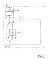
- FIG 1 discloses a photovoltaic system 1, 4, also known as a solar panel system, comprising a photovoltaic source 1 and at least one voltage adding arrangement 4.
- the smallest structural part of a photovoltaic source 1 is a photovoltaic cell consisting of a light absorbing material which is connected to an external circuit.
- a number of photovoltaic cells, conventionally connected in series, constitute a photovoltaic module, which may be used singly or a plurality of them may be connected in series, in parallel or in any combination thereof, into photovoltaic panels.
- a photovoltaic source 1 having a first connector 2 and a second connector 3 according to the invention preferably comprises a photovoltaic module or a plurality of photovoltaic modules.
- the first connector of such a photovoltaic source will in the following be termed input terminal, while the second connector of such a photovoltaic source will be termed output terminal.
- the photovoltaic source 1 is designed to generate an output power at a certain current and a voltage under standard illumination/irradiation present at the location at which the specific photovoltaic system will operate.
- the photovoltaic source 1 is directly dependent on the instantaneous irradiation from the sun, which occasionally may be more or less blocked by clouds which results in that the output voltage of the photovoltaic system will vary over time.
- the photovoltaic system comprises at least one voltage adding arrangement 4, which is connected in series with said photovoltaic source 1.
- the voltage adding arrangement 4 comprises a first connector 5 and a second connector 6, which in the figures is connected to the input terminal 2 of the photovoltaic source 1.
- a voltage adding arrangement may also include a third and a fourth connector.
- the first connector of a voltage adding arrangement will in the following be termed first input terminal, while the second connector of a voltage adding arrangement will be termed output terminal.
- the third and fourth connectors will when they appear be termed second input terminal and third input terminal, respectively.
- the photovoltaic source 1 is located downstream the voltage
- the photovoltaic system is arranged to be connected to a grid, power mains, or the like (not shown), directly or indirectly, in order to supply the output power of the photovoltaic system to a user.
- the voltage adding arrangement 4 comprises a first route 7 and a second route 8 extending between the first input terminal 5 and the output terminal 6 of the voltage adding arrangement 4.
- the first route 7 comprises a voltage source, generally designated 9, and the second route 8 constitutes a voltage source bypass, the first route 7 and the second route 8 being alternately activateable.
- the voltage adding arrangement 4 comprises a common route switch 10 for the first route 7 and the second route 8.
- the first route 7 and the second route 8 may comprise separate route switches (not shown), but it should be pointed out that only one of the first route 7 and the second route 8 shall be active at the same time, in order not to short circuit the voltage source 9. Both the first route 7 and the second route 8 may be inactive at the same time.
- the photovoltaic system When the second route 8 is active the photovoltaic system is in a first mode of operation, in which the output voltage of the photovoltaic system is equal to the output voltage of the photovoltaic source 1, some structural losses may nevertheless occur.
- the first route 7 When the first route 7 is active the photovoltaic system is in a second mode of operation, in which the output voltage of the photovoltaic system is equal to the sum of the output voltage of the photovoltaic source 1 and the output voltage of the voltage adding arrangement 4, some structural losses may nevertheless occur.
- the photovoltaic system switches preferably from the first mode of operation to the second mode of operation when the output voltage of the photovoltaic source 1 decreases below a predetermined threshold value, and vice versa.
- the instantaneous need of output voltage from the photovoltaic system may be considered to raise or lower said threshold values.
- the voltage source 9 may be a fixed voltage source, e.g. a battery, a plurality of batteries, a fuel cell, or the like, or a regulated voltage source, e.g. a set of batteries, or an arrangement comprising a regulator and a fixed voltage source, or the like.
- a fixed voltage source e.g. a battery, a plurality of batteries, a fuel cell, or the like
- a regulated voltage source e.g. a set of batteries, or an arrangement comprising a regulator and a fixed voltage source, or the like.
- the disclosed regulated voltage source 9 comprises four batteries 11a, 11b, 11c, 11d, a bypass arrangement 12 of the first route 7 and three switches 13b, 13c, 13d.
- the default position of each switch 13b, 13c, 13d is in a disconnected position with regard to the corresponding battery 11b, 11c, 11d.
- the switch that at the present is the lowest switch being in the disconnected position also has to be connected to the bypass arrangement 12.
- all switches 13b, 13c, 13d may be connected to the bypass arrangement 12 when in the disconnected positions.
- the switches 13b, 13c, 13d By connecting the switches 13b, 13c, 13d to the corresponding batteries 11b, 11c, 11d, from below and upwards, a stepwise increase of the output voltage from the regulated voltage source 9 is made, depending on the instantaneous need of added voltage to the output voltage of the photovoltaic system.
- the batteries 11a, 11b, 11c, 11d are individually connectable in series with the first route 7 and with each other, and other structural combinations are thus conceivable.
- the photovoltaic system 1, 4 disclosed by figures 3 , 4 , 5 is constituted by the photovoltaic system as illustrated in connection with figure 1 in which the voltage adding arrangement 4 further comprises a charger device 14 connected to the voltage source 9 of the first route 7 and the voltage source 9 is a rechargeable voltage source.
- the charger device 14 comprises a first input terminal 15 and a second input terminal 16, at least one of which being connected to a charger switch 17.
- the charger device 14 has an inactive mode when the first route 7 of the voltage adding arrangement 4 is active and the charger switch 17 is open, and a charging mode when the second route 8 of the voltage adding arrangement 4 is active and the charger switch 17 is closed.
- the use of a charging device 14 implies that the voltage source 9 is rechargeable.
- the voltage source 9 may as a basis only be charged when there is no voltage output therefrom. However, if the voltage source 9 comprises a set of batteries the, at the present, unused batteries may be charged even if there is a voltage output from the voltage source 9. Thus, when the photovoltaic system is in the abovementioned first mode of operation the charging device 14 may be in either the inactive mode or the charging mode, and when the photovoltaic system is in the abovementioned second mode of operation the charging device 14 must be in the inactive mode.
- the charger device is constituted by a DC/DC converter 14, or the like, the first input terminal 15 of which is connected to a second input terminal 18 of the voltage adding arrangement 4, which second input terminal 18 is connected to the first input terminal 5 of the voltage adding arrangement 4.
- the second input terminal 16 of the DC/DC converter 14 is connected to a third input terminal 19 of the voltage adding arrangement 4, which third input terminal 19 is connected to the output terminal 3 of the photovoltaic source 1.
- the first input terminal 15 of the DC/DC converter 14 may be connected directly to the first input terminal 5 of the voltage adding arrangement or to the input terminal 2 of the photovoltaic source 1, and the second input terminal 16 of the DC/DC converter 14 may be connected directly to the output terminal 3 of the photovoltaic source 1.
- the output voltage from the photovoltaic source 1 is used to charge the voltage source 9.
- the DC/DC converter 14 may be put in charging mode when the capability of the voltage source 9 reaches a predetermined level and/or when there is a surplus of energy from the photovoltaic source 1 with regards to the required output voltage of the photovoltaic system.
- the charger device is constituted by a AC/DC converter or a DC/DC converter 14, the first input terminal 15 of which is connected to the second input terminal 18 of the voltage adding arrangement 4.
- the second input terminal 16 of the AC/DC converter or the DC/DC converter 14 is connected to the third input terminal 19 of the voltage adding arrangement 4.
- Said second input terminal 18 and third input terminal 19 of the voltage adding arrangement 4 is connectable to an external power source 20, e.g. a grid, power mains, a motor, a generator, or the like.
- the charging device 14 shall be constituted by a AC/DC converter 14, or the like, and if the external power source 20 is a DC power source the charging device shall be constituted by a DC/DC converter 14, or the like.
- the external power source 20 is used to charge the voltage source 9.
- the AC/DC converter or the DC/DC converter 14 may be put in charging mode when the capability of the voltage source 9 reaches a predetermined level and/or when there is no voltage output from the voltage source 9.
- the charging device 14 is set in charging mode during the night, when a slower charging of the voltage source 9 is admitted and thus a smaller charging device 14 is required.
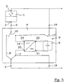
- figure 5 discloses a third embodiment of the present invention.
- the voltage adding arrangement 4 in the shown embodiment comprises a regulated voltage source 9'.
- Said regulated voltage source 9' comprises a voltage source 9 and a charger device 14'.
- the charger device 14' is constituted by a bidirectional DC/DC converter, or the like, and the voltage source 9 is preferably a fixed voltage source, e.g. a battery, or in it self a regulated voltage source, e.g. as disclosed in connection with figure 2 .
- the voltage source 9 is connected to a first input terminal 21 and to a second input terminal 22 of the bidirectional DC/DC converter 14', a first output terminal 23 of the bidirectional DC/DC converter 14' being connected to the first input terminal 5 of the voltage adding arrangement 4, and a second output terminal 24 of the bidirectional DC/DC converter 14' being connected to the first route 7, at the opposite side of the route switch 10 than the output terminal 6 of the voltage adding arrangement 4, and being connected by means of a charger switch 17 to the third input terminal 19 of the voltage adding arrangement 4, which third input terminal 19 is connected to the output terminal 3 of the photovoltaic source 1.
- first output terminal 23 of the bidirectional DC/DC converter 14' may as well be connected to the second input terminal 18 of the voltage adding arrangement 4, and the second output terminal 24 of the bidirectional DC/DC converter 14' may be connected by means of the charger switch 17 directly to the output terminal 3 of the photovoltaic source 1.
- the bidirectional DC/DC converter 14' has a regulator mode when the first route 7 of the voltage adding arrangement 4 is active and the charger switch 17 is open, and a charging mode when the second route 8 of the voltage adding arrangement 4 is active and the charger switch 17 is closed.
- the output voltage from the voltage source may in theory be everything between 0% and 100% of the capacity of the voltage source 9, or even higher than 100% if the regulator is of a suitable boost converter type, some structural losses may nevertheless occur.
- the bidirectional DC/DC converter 14' may be in either the regulator mode or in the charging mode, and when the photovoltaic system is in the abovementioned second mode of operation the bidirectional DC/DC converter 14' must be in the regulator mode.
- the bidirectional DC/DC converter 14' may be put in charging mode when the capacity of the voltage source 9 reaches a predetermined level and/or when there is a surplus of energy from the photovoltaic source 1 with regards to the required output voltage of the photovoltaic system.
- the bidirectional DC/DC converter 14' could be exchanged by a device only capable of regulating the output voltage of the voltage source 9. Then the second output terminal 24 of that device should not be connected to the third input terminal 19 of the voltage adding arrangement 4.
- a separate charging device e.g. as disclosed in connection with the first and second embodiments according to figures 3 and 4 , respectively, could be used. That is, such an alternative should be constituted by said first or second embodiment of the present invention having a regulated voltage source with a continuously variable output voltage.
- all switches preferably is controlled by a control system (not shown) which for instance may supervise the instantaneous capacity of the voltage source, the instantaneous output voltage from the photovoltaic source, the instantaneous irradiation, etc.
- the capacity of the voltage source may be a part of, equal to, or more than, the capacity of the photovoltaic source, all depending on the specific application. If the photovoltaic system is expected to have an output voltage during long cloudy periods or during the nights, the capacity of the voltage source should preferably be equal to or more than the capacity of the photovoltaic source. If the voltage source is expected only to support the photovoltaic source during short periods of decreased irradiation, the capacity of the voltage source could for instance be about 10-40% 11 capacity of the photovoltaic source.
- the charging devices according to the first and third embodiments of the present invention should be connected to the input terminal of the photovoltaic source and to the output terminal of the voltage adding arrangement.
- photovoltaic sources and/or voltage adding arrangements may be connected to the inventive photovoltaic system in parallel, in series, or in any combination thereof.
- a common charger device may be used to charge several voltage sources.
Landscapes
- Engineering & Computer Science (AREA)
- Power Engineering (AREA)
- Charge And Discharge Circuits For Batteries Or The Like (AREA)
- Photovoltaic Devices (AREA)
- Secondary Cells (AREA)
Claims (12)
- Système photovoltaïque permettant de générer une tension de sortie essentiellement insensible aux variations de rayonnement, le système photovoltaïque comprenant une source photovoltaïque (1) possédant une borne négative (2) et une borne positive (3), le système photovoltaïque comprenant un montage additionneur de tension (4) comprenant une première borne négative (5) et une borne positive (6), le montage additionneur de tension (4) étant relié en série avec la source photovoltaïque (1), et un premier chemin (7) comprenant une source de tension rechargeable (9, 9') et un deuxième chemin (8) constituant une dérivation de source de tension s'étendant entre ladite première borne négative (5) et ladite borne positive (6) du montage additionneur de tension (4), lesdits premier et deuxième chemins étant activables en alternance,
caractérisé en ce que le montage additionneur de tension (4) comprend en outre un commutateur (17) de chargeur et un dispositif chargeur (14, 14') relié à la source de tension (9, 9') du premier chemin (7), le dispositif chargeur (14, 14') comprenant une première borne d'entrée (15) et une deuxième borne d'entrée (16) dont une au moins est reliée au commutateur (17) de chargeur par le biais duquel le dispositif chargeur (14, 14') peut être relié à la source photovoltaïque (1) ou à une source d'alimentation externe (20) afin de charger la source de tension (9, 9'). - Système photovoltaïque selon la revendication 1, la source photovoltaïque (1) étant constituée d'un module photovoltaïque ou d'une pluralité de modules photovoltaïques.
- Système photovoltaïque selon la revendication 1 ou 2, le montage additionneur de tension (4) comprenant un commutateur commun (10) de chemin pour le premier chemin (7) et le deuxième chemin (8).
- Système photovoltaïque selon la revendication 1 ou 2, le premier chemin (7) et le deuxième chemin (8) du montage additionneur de tension (4) comprenant des commutateurs de chemin distincts.
- Système photovoltaïque selon l'une quelconque des revendications précédentes, la source de tension (9, 9') étant constituée d'une source de tension fixe ou d'une source de tension régulée.
- Système photovoltaïque selon l'une quelconque des revendications précédentes, la source de tension (9) étant constituée d'au moins une batterie.
- Système photovoltaïque selon l'une quelconque des revendications précédentes, la source de tension (9) comprenant au moins deux batteries (11a, 11b, 11c, 11d) susceptibles d'être individuellement reliées en série avec le premier chemin (7) et l'une (les unes) avec l'autre (les autres).
- Système photovoltaïque selon l'une quelconque des revendications précédentes, le dispositif chargeur (14) possédant un mode inactif lorsque le commutateur (17) de chargeur est ouvert, et un mode de charge lorsque le deuxième chemin (8) du montage additionneur de tension (4) est actif et le commutateur (17) de chargeur est fermé.
- Système photovoltaïque selon l'une quelconque des revendications précédentes, le dispositif chargeur (14) étant constitué d'un convertisseur continu-continu dont la première borne d'entrée (15) est reliée, directement ou indirectement, à la borne d'entrée (2) de la source photovoltaïque (1) et dont la deuxième borne d'entrée (16) est reliée, directement ou indirectement, à la borne de sortie (3) de la source photovoltaïque (1).
- Système photovoltaïque selon l'une quelconque des revendications 1 à 8, le dispositif chargeur (14) étant constitué d'un convertisseur alternatif-continu ou d'un convertisseur continu-continu dont la première borne d'entrée (15) est reliée à une deuxième borne d'entrée (18) du montage additionneur de tension (4) et dont la deuxième borne d'entrée (16) est reliée à une troisième borne d'entrée (19) du montage additionneur de tension (4), lesdites deuxième et troisième bornes d'entrée du montage additionneur de tension (4) étant susceptibles d'être reliées à une source d'alimentation externe (20).
- Système photovoltaïque selon l'une quelconque des revendications 1 à 7, le montage additionneur de tension (4) comprenant une source de tension régulée (9') comprenant une source de tension (9) et un dispositif chargeur (14'), lequel dispositif chargeur (14') est constitué d'un convertisseur continu-continu bidirectionnel, la source de tension (9) étant reliée à une première borne d'entrée (21) et à une deuxième borne d'entrée (22) du convertisseur continu-continu bidirectionnel (14'), une première borne de sortie (23) du convertisseur continu-continu bidirectionnel (14') étant reliée à la première borne d'entrée (5) du montage additionneur de tension (4), et une deuxième borne de sortie (24) du convertisseur continu-continu bidirectionnel (14') étant reliée au premier chemin (7) du côté du commutateur (10) de chemin opposé à celui de la borne de sortie (6) du montage additionneur de tension (4), et étant reliée par le biais d'un commutateur (17) de chargeur, directement ou indirectement, à la borne de sortie (3) de la source photovoltaïque (1).
- Système photovoltaïque selon la revendication 11, le convertisseur continu-continu bidirectionnel (14') possédant un mode de régulation lorsque le premier chemin (7) du montage additionneur de tension (4) est actif et le commutateur (17) de chargeur est ouvert, et un mode de charge lorsque le deuxième chemin (8) du montage additionneur de tension (4) est actif et le commutateur (17) de chargeur est fermé.
Priority Applications (9)
| Application Number | Priority Date | Filing Date | Title |
|---|---|---|---|
| ES08172418T ES2381227T3 (es) | 2008-12-19 | 2008-12-19 | Un sistema fotovoltaico |
| AT08172418T ATE544223T1 (de) | 2008-12-19 | 2008-12-19 | Photovoltaiksystem |
| EP20080172418 EP2200152B1 (fr) | 2008-12-19 | 2008-12-19 | Système photovoltaïque |
| AU2009329553A AU2009329553B2 (en) | 2008-12-19 | 2009-12-18 | A photovoltaic system |
| AU2009329554A AU2009329554B2 (en) | 2008-12-19 | 2009-12-18 | A photovoltaic system |
| PCT/EP2009/067568 WO2010070115A2 (fr) | 2008-12-19 | 2009-12-18 | Système photovoltaïque |
| PCT/EP2009/067565 WO2010070114A2 (fr) | 2008-12-19 | 2009-12-18 | Système photovoltaïque |
| CN200980151594.3A CN102257699B (zh) | 2008-12-19 | 2009-12-18 | 光伏系统 |
| US13/163,173 US8643323B2 (en) | 2008-12-19 | 2011-06-17 | Photovoltaic system |
Applications Claiming Priority (1)
| Application Number | Priority Date | Filing Date | Title |
|---|---|---|---|
| EP20080172418 EP2200152B1 (fr) | 2008-12-19 | 2008-12-19 | Système photovoltaïque |
Publications (2)
| Publication Number | Publication Date |
|---|---|
| EP2200152A1 EP2200152A1 (fr) | 2010-06-23 |
| EP2200152B1 true EP2200152B1 (fr) | 2012-02-01 |
Family
ID=40627640
Family Applications (1)
| Application Number | Title | Priority Date | Filing Date |
|---|---|---|---|
| EP20080172418 Not-in-force EP2200152B1 (fr) | 2008-12-19 | 2008-12-19 | Système photovoltaïque |
Country Status (7)
| Country | Link |
|---|---|
| US (1) | US8643323B2 (fr) |
| EP (1) | EP2200152B1 (fr) |
| CN (1) | CN102257699B (fr) |
| AT (1) | ATE544223T1 (fr) |
| AU (2) | AU2009329554B2 (fr) |
| ES (1) | ES2381227T3 (fr) |
| WO (2) | WO2010070114A2 (fr) |
Families Citing this family (11)
| Publication number | Priority date | Publication date | Assignee | Title |
|---|---|---|---|---|
| DE102010016138A1 (de) * | 2010-03-25 | 2011-09-29 | Refu Elektronik Gmbh | Solarwechselrichter für erweiterten Einstrahlungswertebereich und Betriebsverfahren |
| EP2461456B1 (fr) | 2010-12-03 | 2014-07-02 | ABB Oy | Conversion CA de tension CC variable tel qu'une alimentation solaire |
| GB2487419B (en) * | 2011-01-24 | 2012-12-19 | Alexander John Topping | Method for solar cell assembly with increased operational power output |
| US9073937B2 (en) | 2011-06-16 | 2015-07-07 | Board Of Trustees Of The University Of Alabama | Organic photovoltaic-battery hybrid device |
| DE102012002599B4 (de) * | 2012-02-13 | 2016-03-03 | Refusol Gmbh | Energieerzeugungsanlage mit Wechselrichter und Energiespeichersystem |
| EP2773036B1 (fr) * | 2013-02-27 | 2016-02-24 | Optistring Technologies AB | Procédé de conversion CC-CA |
| US10199832B2 (en) * | 2015-04-28 | 2019-02-05 | First Solar, Inc. | Photovoltaic DC power distribution system |
| FR3036866B1 (fr) | 2015-05-25 | 2018-09-07 | Commissariat A L'energie Atomique Et Aux Energies Alternatives | Optimisation de la recuperation energetique solaire photovoltaique |
| EP3398239A1 (fr) * | 2015-12-29 | 2018-11-07 | Vito NV | Dispositif et procédé de reconfiguration d'un dispositif de stockage d'énergie rechargeable en chaînes de connexion de batteries séparées |
| FI129503B (en) | 2018-05-29 | 2022-03-31 | L7 Drive Oy | Adaptive DC-DC converter for use with a loader and charger |
| CN117748977B (zh) * | 2023-12-26 | 2024-12-17 | 北京索英电气技术股份有限公司 | 一种光伏逆变器和光伏发电系统 |
Family Cites Families (15)
| Publication number | Priority date | Publication date | Assignee | Title |
|---|---|---|---|---|
| CH617822B (fr) * | 1975-12-10 | Ebauches Sa | Dispositif permettant de recharger un accumulateur a l'aide d'elements photosensibles. | |
| CH594306A5 (fr) * | 1976-05-21 | 1978-01-13 | Ebauches Sa | |
| US5327071A (en) | 1991-11-05 | 1994-07-05 | The United States Of America As Represented By The Administrator Of The National Aeronautics & Space Administration | Microprocessor control of multiple peak power tracking DC/DC converters for use with solar cell arrays |
| DE4204237A1 (de) * | 1992-02-13 | 1993-08-19 | Grundig Emv | Solar-ladestation fuer diktiergeraete |
| US5929538A (en) * | 1997-06-27 | 1999-07-27 | Abacus Controls Inc. | Multimode power processor |
| GB9725128D0 (en) * | 1997-11-27 | 1998-01-28 | Weinberg Alan H | Solar array system |
| US6034506A (en) * | 1998-01-16 | 2000-03-07 | Space Systems/Loral, Inc. | Lithium ion satellite battery charge control circuit |
| US6599655B2 (en) * | 2001-04-06 | 2003-07-29 | The Boeing Company | Procedure for performing battery reconditioning on a space vehicle designed with one battery |
| US6768047B2 (en) * | 2002-06-13 | 2004-07-27 | Koninklijke Philips Electronics N.V. | Autonomous solid state lighting system |
| NL1027247C2 (nl) * | 2004-10-14 | 2006-04-19 | Tendris Solutions Bv | Inrichting en werkwijze voor het laden van een accumulator. |
| DE102005017835B3 (de) | 2005-04-18 | 2006-11-23 | Beck Energy Gmbh | Photovoltaikgenerator mit Thermoschalterelement |
| EP1901414B1 (fr) * | 2006-09-15 | 2009-07-08 | ERGOBIONIK GmbH | Commande pour une illumination alimentée par énergie solaire |
| US7812247B2 (en) | 2006-10-23 | 2010-10-12 | Ascent Solar Technologies Inc. | Flexible photovoltaic array with integrated wiring and control circuitry, and associated methods |
| WO2008064605A1 (fr) * | 2006-11-30 | 2008-06-05 | Beijing Hi-Tech Wealth Investment & Development Co., Ltd | Procédé, appareil et système permettant de fournir de l'énergie à l'aide de cellules photovoltaïques |
| CN100468912C (zh) * | 2007-05-15 | 2009-03-11 | 北京恒基伟业投资发展有限公司 | 非对称蓄电池组、具有该电池组的太阳能电池及充放电法 |
-
2008
- 2008-12-19 EP EP20080172418 patent/EP2200152B1/fr not_active Not-in-force
- 2008-12-19 AT AT08172418T patent/ATE544223T1/de active
- 2008-12-19 ES ES08172418T patent/ES2381227T3/es active Active
-
2009
- 2009-12-18 AU AU2009329554A patent/AU2009329554B2/en not_active Ceased
- 2009-12-18 WO PCT/EP2009/067565 patent/WO2010070114A2/fr not_active Ceased
- 2009-12-18 AU AU2009329553A patent/AU2009329553B2/en not_active Ceased
- 2009-12-18 CN CN200980151594.3A patent/CN102257699B/zh active Active
- 2009-12-18 WO PCT/EP2009/067568 patent/WO2010070115A2/fr not_active Ceased
-
2011
- 2011-06-17 US US13/163,173 patent/US8643323B2/en active Active
Also Published As
| Publication number | Publication date |
|---|---|
| AU2009329553B2 (en) | 2013-07-11 |
| WO2010070114A2 (fr) | 2010-06-24 |
| CN102257699B (zh) | 2015-01-07 |
| ATE544223T1 (de) | 2012-02-15 |
| AU2009329553A1 (en) | 2011-06-23 |
| WO2010070115A4 (fr) | 2010-11-25 |
| ES2381227T3 (es) | 2012-05-24 |
| AU2009329554B2 (en) | 2013-05-02 |
| CN102257699A (zh) | 2011-11-23 |
| WO2010070115A2 (fr) | 2010-06-24 |
| WO2010070115A3 (fr) | 2010-10-07 |
| EP2200152A1 (fr) | 2010-06-23 |
| US8643323B2 (en) | 2014-02-04 |
| WO2010070114A3 (fr) | 2010-09-16 |
| US20120025751A1 (en) | 2012-02-02 |
| WO2010070114A4 (fr) | 2010-11-18 |
| AU2009329554A1 (en) | 2010-06-24 |
Similar Documents
| Publication | Publication Date | Title |
|---|---|---|
| EP2200152B1 (fr) | Système photovoltaïque | |
| US8629648B2 (en) | Photovoltaic system | |
| US20130099581A1 (en) | Energy Storage System | |
| US20150048794A1 (en) | Battery charge balancing device and battery charge balancing system | |
| JP5541982B2 (ja) | 直流配電システム | |
| WO2017161059A9 (fr) | Système et procédé de régulation de cc symétrique pour génération et stockage optimisés d'énergie solaire | |
| Jing et al. | Smart hybrid energy storage for stand-alone PV microgrid: Optimization of battery lifespan through dynamic power allocation | |
| CN108054826B (zh) | 一种防冲击电流蓄电池保护的光储系统 | |
| Hassan et al. | CONTROL AND ENERGY MANAGEMENT SCHEME FOR A PV/SC/BATTERY HYBRID RENEWABLE POWER SYSTEM. | |
| Zhou et al. | Hybrid diesel/MCT/battery electricity power supply system for power management in small islanded sites: case study for the ouessant French island | |
| CN102983617B (zh) | 具有适应性电能控制的太阳光伏发电系统及其操作方法 | |
| Gawande et al. | Design and development of cost-effective solar PV based DC microgrid for rural applications | |
| Cavallaro et al. | Smart photovoltaic UPS system for domestic appliances | |
| KR101929974B1 (ko) | 태양광 발전시스템 | |
| CN223872051U (zh) | 光伏储能系统 | |
| Remache et al. | Predictive Power Control and Power Management for Islanded PV Microgrid with Battery-Supercapacitor Hybrid Energy Storage System | |
| Ramya et al. | A novel multi input DC-DC converter for integrated wind, PV renewable energy generated system | |
| CN114977294B (zh) | 一种光储系统及控制方法 | |
| CN210468881U (zh) | 一种太阳能转换器 | |
| KR20150029809A (ko) | 계통 연계형 태양광발전 장치 | |
| CN111464111B (zh) | 一种太阳能发电智能控制系统 | |
| Meshram et al. | Design and Development of MPPT based Converter for Efficient Solar Power Conversion | |
| Srinivasan et al. | Advanced Energy Management via Integrated Converter in PV-Wind Hybrid Storage-Based DC Microgrids | |
| Choi et al. | Large-scale PV systems with energy storage utilizing high-gain DC/DC converters | |
| Chandra et al. | Empowering Renewable Energy: The Role of Battery Storage and Digital Platforms in Solar PV Systems |
Legal Events
| Date | Code | Title | Description |
|---|---|---|---|
| PUAI | Public reference made under article 153(3) epc to a published international application that has entered the european phase |
Free format text: ORIGINAL CODE: 0009012 |
|
| 17P | Request for examination filed |
Effective date: 20081221 |
|
| AK | Designated contracting states |
Kind code of ref document: A1 Designated state(s): AT BE BG CH CY CZ DE DK EE ES FI FR GB GR HR HU IE IS IT LI LT LU LV MC MT NL NO PL PT RO SE SI SK TR |
|
| AX | Request for extension of the european patent |
Extension state: AL BA MK RS |
|
| AKX | Designation fees paid |
Designated state(s): AT BE BG CH CY CZ DE DK EE ES FI FR GB GR HR HU IE IS IT LI LT LU LV MC MT NL NO PL PT RO SE SI SK TR |
|
| GRAP | Despatch of communication of intention to grant a patent |
Free format text: ORIGINAL CODE: EPIDOSNIGR1 |
|
| GRAS | Grant fee paid |
Free format text: ORIGINAL CODE: EPIDOSNIGR3 |
|
| RIN1 | Information on inventor provided before grant (corrected) |
Inventor name: NORRGA, STAFFAN Inventor name: THORBURN, STEFAN Inventor name: BAKAS, PANAGIOTIS Inventor name: PAPASTERGIOU, KONSTANTINOS Inventor name: DEMETRIADES, GEORGIOS Inventor name: DIJKHUIZEN, FRANS Inventor name: AENGQUIST, LENNART Inventor name: STRIDH, BENGT |
|
| GRAA | (expected) grant |
Free format text: ORIGINAL CODE: 0009210 |
|
| AK | Designated contracting states |
Kind code of ref document: B1 Designated state(s): AT BE BG CH CY CZ DE DK EE ES FI FR GB GR HR HU IE IS IT LI LT LU LV MC MT NL NO PL PT RO SE SI SK TR |
|
| REG | Reference to a national code |
Ref country code: GB Ref legal event code: FG4D |
|
| REG | Reference to a national code |
Ref country code: AT Ref legal event code: REF Ref document number: 544223 Country of ref document: AT Kind code of ref document: T Effective date: 20120215 Ref country code: CH Ref legal event code: EP |
|
| REG | Reference to a national code |
Ref country code: DE Ref legal event code: R096 Ref document number: 602008013057 Country of ref document: DE Effective date: 20120329 |
|
| REG | Reference to a national code |
Ref country code: ES Ref legal event code: FG2A Ref document number: 2381227 Country of ref document: ES Kind code of ref document: T3 Effective date: 20120524 |
|
| REG | Reference to a national code |
Ref country code: NL Ref legal event code: VDEP Effective date: 20120201 |
|
| LTIE | Lt: invalidation of european patent or patent extension |
Effective date: 20120201 |
|
| PG25 | Lapsed in a contracting state [announced via postgrant information from national office to epo] |
Ref country code: LT Free format text: LAPSE BECAUSE OF FAILURE TO SUBMIT A TRANSLATION OF THE DESCRIPTION OR TO PAY THE FEE WITHIN THE PRESCRIBED TIME-LIMIT Effective date: 20120201 Ref country code: NO Free format text: LAPSE BECAUSE OF FAILURE TO SUBMIT A TRANSLATION OF THE DESCRIPTION OR TO PAY THE FEE WITHIN THE PRESCRIBED TIME-LIMIT Effective date: 20120501 Ref country code: NL Free format text: LAPSE BECAUSE OF FAILURE TO SUBMIT A TRANSLATION OF THE DESCRIPTION OR TO PAY THE FEE WITHIN THE PRESCRIBED TIME-LIMIT Effective date: 20120201 Ref country code: HR Free format text: LAPSE BECAUSE OF FAILURE TO SUBMIT A TRANSLATION OF THE DESCRIPTION OR TO PAY THE FEE WITHIN THE PRESCRIBED TIME-LIMIT Effective date: 20120201 Ref country code: IS Free format text: LAPSE BECAUSE OF FAILURE TO SUBMIT A TRANSLATION OF THE DESCRIPTION OR TO PAY THE FEE WITHIN THE PRESCRIBED TIME-LIMIT Effective date: 20120601 |
|
| PG25 | Lapsed in a contracting state [announced via postgrant information from national office to epo] |
Ref country code: PL Free format text: LAPSE BECAUSE OF FAILURE TO SUBMIT A TRANSLATION OF THE DESCRIPTION OR TO PAY THE FEE WITHIN THE PRESCRIBED TIME-LIMIT Effective date: 20120201 Ref country code: GR Free format text: LAPSE BECAUSE OF FAILURE TO SUBMIT A TRANSLATION OF THE DESCRIPTION OR TO PAY THE FEE WITHIN THE PRESCRIBED TIME-LIMIT Effective date: 20120502 Ref country code: BE Free format text: LAPSE BECAUSE OF FAILURE TO SUBMIT A TRANSLATION OF THE DESCRIPTION OR TO PAY THE FEE WITHIN THE PRESCRIBED TIME-LIMIT Effective date: 20120201 Ref country code: LV Free format text: LAPSE BECAUSE OF FAILURE TO SUBMIT A TRANSLATION OF THE DESCRIPTION OR TO PAY THE FEE WITHIN THE PRESCRIBED TIME-LIMIT Effective date: 20120201 Ref country code: FI Free format text: LAPSE BECAUSE OF FAILURE TO SUBMIT A TRANSLATION OF THE DESCRIPTION OR TO PAY THE FEE WITHIN THE PRESCRIBED TIME-LIMIT Effective date: 20120201 Ref country code: PT Free format text: LAPSE BECAUSE OF FAILURE TO SUBMIT A TRANSLATION OF THE DESCRIPTION OR TO PAY THE FEE WITHIN THE PRESCRIBED TIME-LIMIT Effective date: 20120601 |
|
| REG | Reference to a national code |
Ref country code: AT Ref legal event code: MK05 Ref document number: 544223 Country of ref document: AT Kind code of ref document: T Effective date: 20120201 |
|
| PG25 | Lapsed in a contracting state [announced via postgrant information from national office to epo] |
Ref country code: CY Free format text: LAPSE BECAUSE OF FAILURE TO SUBMIT A TRANSLATION OF THE DESCRIPTION OR TO PAY THE FEE WITHIN THE PRESCRIBED TIME-LIMIT Effective date: 20120201 |
|
| PG25 | Lapsed in a contracting state [announced via postgrant information from national office to epo] |
Ref country code: RO Free format text: LAPSE BECAUSE OF FAILURE TO SUBMIT A TRANSLATION OF THE DESCRIPTION OR TO PAY THE FEE WITHIN THE PRESCRIBED TIME-LIMIT Effective date: 20120201 Ref country code: CZ Free format text: LAPSE BECAUSE OF FAILURE TO SUBMIT A TRANSLATION OF THE DESCRIPTION OR TO PAY THE FEE WITHIN THE PRESCRIBED TIME-LIMIT Effective date: 20120201 Ref country code: SI Free format text: LAPSE BECAUSE OF FAILURE TO SUBMIT A TRANSLATION OF THE DESCRIPTION OR TO PAY THE FEE WITHIN THE PRESCRIBED TIME-LIMIT Effective date: 20120201 Ref country code: EE Free format text: LAPSE BECAUSE OF FAILURE TO SUBMIT A TRANSLATION OF THE DESCRIPTION OR TO PAY THE FEE WITHIN THE PRESCRIBED TIME-LIMIT Effective date: 20120201 Ref country code: DK Free format text: LAPSE BECAUSE OF FAILURE TO SUBMIT A TRANSLATION OF THE DESCRIPTION OR TO PAY THE FEE WITHIN THE PRESCRIBED TIME-LIMIT Effective date: 20120201 Ref country code: SE Free format text: LAPSE BECAUSE OF FAILURE TO SUBMIT A TRANSLATION OF THE DESCRIPTION OR TO PAY THE FEE WITHIN THE PRESCRIBED TIME-LIMIT Effective date: 20120201 |
|
| PG25 | Lapsed in a contracting state [announced via postgrant information from national office to epo] |
Ref country code: SK Free format text: LAPSE BECAUSE OF FAILURE TO SUBMIT A TRANSLATION OF THE DESCRIPTION OR TO PAY THE FEE WITHIN THE PRESCRIBED TIME-LIMIT Effective date: 20120201 |
|
| PLBE | No opposition filed within time limit |
Free format text: ORIGINAL CODE: 0009261 |
|
| STAA | Information on the status of an ep patent application or granted ep patent |
Free format text: STATUS: NO OPPOSITION FILED WITHIN TIME LIMIT |
|
| 26N | No opposition filed |
Effective date: 20121105 |
|
| PG25 | Lapsed in a contracting state [announced via postgrant information from national office to epo] |
Ref country code: AT Free format text: LAPSE BECAUSE OF FAILURE TO SUBMIT A TRANSLATION OF THE DESCRIPTION OR TO PAY THE FEE WITHIN THE PRESCRIBED TIME-LIMIT Effective date: 20120201 |
|
| REG | Reference to a national code |
Ref country code: DE Ref legal event code: R097 Ref document number: 602008013057 Country of ref document: DE Effective date: 20121105 |
|
| PG25 | Lapsed in a contracting state [announced via postgrant information from national office to epo] |
Ref country code: MC Free format text: LAPSE BECAUSE OF NON-PAYMENT OF DUE FEES Effective date: 20121231 Ref country code: BG Free format text: LAPSE BECAUSE OF FAILURE TO SUBMIT A TRANSLATION OF THE DESCRIPTION OR TO PAY THE FEE WITHIN THE PRESCRIBED TIME-LIMIT Effective date: 20120501 |
|
| REG | Reference to a national code |
Ref country code: CH Ref legal event code: PL |
|
| GBPC | Gb: european patent ceased through non-payment of renewal fee |
Effective date: 20121219 |
|
| REG | Reference to a national code |
Ref country code: IE Ref legal event code: MM4A |
|
| PG25 | Lapsed in a contracting state [announced via postgrant information from national office to epo] |
Ref country code: CH Free format text: LAPSE BECAUSE OF NON-PAYMENT OF DUE FEES Effective date: 20121231 Ref country code: IE Free format text: LAPSE BECAUSE OF NON-PAYMENT OF DUE FEES Effective date: 20121219 Ref country code: LI Free format text: LAPSE BECAUSE OF NON-PAYMENT OF DUE FEES Effective date: 20121231 |
|
| PG25 | Lapsed in a contracting state [announced via postgrant information from national office to epo] |
Ref country code: GB Free format text: LAPSE BECAUSE OF NON-PAYMENT OF DUE FEES Effective date: 20121219 Ref country code: MT Free format text: LAPSE BECAUSE OF FAILURE TO SUBMIT A TRANSLATION OF THE DESCRIPTION OR TO PAY THE FEE WITHIN THE PRESCRIBED TIME-LIMIT Effective date: 20120201 |
|
| PG25 | Lapsed in a contracting state [announced via postgrant information from national office to epo] |
Ref country code: TR Free format text: LAPSE BECAUSE OF FAILURE TO SUBMIT A TRANSLATION OF THE DESCRIPTION OR TO PAY THE FEE WITHIN THE PRESCRIBED TIME-LIMIT Effective date: 20120201 |
|
| PG25 | Lapsed in a contracting state [announced via postgrant information from national office to epo] |
Ref country code: LU Free format text: LAPSE BECAUSE OF NON-PAYMENT OF DUE FEES Effective date: 20121219 |
|
| PG25 | Lapsed in a contracting state [announced via postgrant information from national office to epo] |
Ref country code: HU Free format text: LAPSE BECAUSE OF FAILURE TO SUBMIT A TRANSLATION OF THE DESCRIPTION OR TO PAY THE FEE WITHIN THE PRESCRIBED TIME-LIMIT Effective date: 20081219 |
|
| REG | Reference to a national code |
Ref country code: FR Ref legal event code: PLFP Year of fee payment: 8 |
|
| REG | Reference to a national code |
Ref country code: FR Ref legal event code: PLFP Year of fee payment: 9 |
|
| PGFP | Annual fee paid to national office [announced via postgrant information from national office to epo] |
Ref country code: DE Payment date: 20161213 Year of fee payment: 9 |
|
| PGFP | Annual fee paid to national office [announced via postgrant information from national office to epo] |
Ref country code: FR Payment date: 20161222 Year of fee payment: 9 Ref country code: ES Payment date: 20161213 Year of fee payment: 9 |
|
| PGFP | Annual fee paid to national office [announced via postgrant information from national office to epo] |
Ref country code: IT Payment date: 20161223 Year of fee payment: 9 |
|
| REG | Reference to a national code |
Ref country code: DE Ref legal event code: R119 Ref document number: 602008013057 Country of ref document: DE |
|
| REG | Reference to a national code |
Ref country code: FR Ref legal event code: ST Effective date: 20180831 |
|
| PG25 | Lapsed in a contracting state [announced via postgrant information from national office to epo] |
Ref country code: FR Free format text: LAPSE BECAUSE OF NON-PAYMENT OF DUE FEES Effective date: 20180102 Ref country code: DE Free format text: LAPSE BECAUSE OF NON-PAYMENT OF DUE FEES Effective date: 20180703 Ref country code: IT Free format text: LAPSE BECAUSE OF NON-PAYMENT OF DUE FEES Effective date: 20171219 |
|
| REG | Reference to a national code |
Ref country code: ES Ref legal event code: FD2A Effective date: 20190703 |
|
| PG25 | Lapsed in a contracting state [announced via postgrant information from national office to epo] |
Ref country code: ES Free format text: LAPSE BECAUSE OF NON-PAYMENT OF DUE FEES Effective date: 20171220 |