EP2201323B1 - Präzisionserhöhungsmechanismus und -verfahren für ein faser-optisches Strommessgerät - Google Patents
Präzisionserhöhungsmechanismus und -verfahren für ein faser-optisches Strommessgerät Download PDFInfo
- Publication number
- EP2201323B1 EP2201323B1 EP08838669.3A EP08838669A EP2201323B1 EP 2201323 B1 EP2201323 B1 EP 2201323B1 EP 08838669 A EP08838669 A EP 08838669A EP 2201323 B1 EP2201323 B1 EP 2201323B1
- Authority
- EP
- European Patent Office
- Prior art keywords
- fiber
- gap
- mirror
- optical fiber
- quarter wave
- Prior art date
- Legal status (The legal status is an assumption and is not a legal conclusion. Google has not performed a legal analysis and makes no representation as to the accuracy of the status listed.)
- Active
Links
Images


Classifications
-
- G—PHYSICS
- G01—MEASURING; TESTING
- G01R—MEASURING ELECTRIC VARIABLES; MEASURING MAGNETIC VARIABLES
- G01R15/00—Details of measuring arrangements of the types provided for in groups G01R17/00 - G01R29/00, G01R33/00 - G01R33/26 or G01R35/00
- G01R15/14—Adaptations providing voltage or current isolation, e.g. for high-voltage or high-current networks
- G01R15/24—Adaptations providing voltage or current isolation, e.g. for high-voltage or high-current networks using light-modulating devices
- G01R15/245—Adaptations providing voltage or current isolation, e.g. for high-voltage or high-current networks using light-modulating devices using magneto-optical modulators, e.g. based on the Faraday or Cotton-Mouton effect
- G01R15/246—Adaptations providing voltage or current isolation, e.g. for high-voltage or high-current networks using light-modulating devices using magneto-optical modulators, e.g. based on the Faraday or Cotton-Mouton effect based on the Faraday, i.e. linear magneto-optic, effect
-
- G—PHYSICS
- G01—MEASURING; TESTING
- G01R—MEASURING ELECTRIC VARIABLES; MEASURING MAGNETIC VARIABLES
- G01R15/00—Details of measuring arrangements of the types provided for in groups G01R17/00 - G01R29/00, G01R33/00 - G01R33/26 or G01R35/00
- G01R15/14—Adaptations providing voltage or current isolation, e.g. for high-voltage or high-current networks
- G01R15/24—Adaptations providing voltage or current isolation, e.g. for high-voltage or high-current networks using light-modulating devices
- G01R15/247—Details of the circuitry or construction of devices covered by G01R15/241 - G01R15/246
Definitions
- This invention relates generally to a device and method for enhancing the accuracy of a current measuring apparatus, and more particularly where the current measuring apparatus uses optical sensing technology.
- Conventional high current (up to about 500 KA) measurement equipment uses Hall effect technology to measure the magnetic field around a conductor. Electricity carried through a conductor produces a magnetic field that varies with current, and conventional measurement equipment uses an electronic sensor (Hall sensor) that varies its output voltage in response to changes in magnetic field density. A Hall sensor in close proximity to the conductor can thus be used to effectively measure the current without interrupting the circuit or making electrical contact with the conductor. Typically, the Hall sensor is integrated with a wound core that surrounds the conductor to be measured. Conventional Hall technology current measuring equipment has the disadvantages of being expensive, large, heavy and time-consuming to install.
- Optical devices can also be used to measure current.
- Such devices are interferometers that utilize the Faraday effect, in which there is an interaction between light and the magnetic field produced around the conductor, to measure current.
- Existing technology for carrying out this measurement does not have sufficient accuracy under all circumstances. The reason for this is explained below.
- An optical interferometer of the type described such as the Fiber Optic Current Sensor made and sold by Nxtphase, works on the principle that the speeds of right handed circularly polarized (RHCP) and left handed circularly polarized (LHCP) light waves are oppositely affected by a magnetic field.
- a fiber optic circuit is arranged in such a way that two beams, one that is RHCP and one that is LHCP, are sent through an optical fiber that extends through the magnetic field around the conductor, and the total phase difference accumulated between the two beams is measured.
- the total phase difference is proportional to the line integral of the magnetic field along the path of the sensing fiber.
- the sensor measures the closed path integral of the magnetic field around the conductor. By Ampere's Law, this is equal to the current carried in the conductor.
- the phase shift caused by the magnetic field is a function of the current flowing in the conductor, and there are two main properties that affect how much phase shift is measured for a given current, also called the "scaling" of the current sensor.
- the first of these is the quality of the quarter wave plate.
- the quarter wave plate defines the beginning of the sensing region, where the beams are polarized, and the end of the sensing region for the returning light.
- An imperfect quarter wave plate gives rise to impure beams, and consequently a change in the scaling of the sensor.
- the properties described above that affect the scaling of the sensor are functions of temperature.
- Current sensors are used for the measurement of large DC currents, and the conductors that carry these currents are large and generate significant heat. Because of this, there can be large temperature gradients around the conductor, which reduces the ability of the current sensor to maintain an accurate scale factor.
- a known fibre-optic current sensor ( BOHNERT K: ET AL; "Highly Accurate Fibre-Optic DC Current Sensor for the Electro-Winning Industry", PETROLEUM ANO CHEMICAL INOUSTRY CONFERENCE, 2005, INDUSTRY APPLICATION'S SOCIETY 52ND ANNUAL DENVER, CO, USA 12-14 SEPT. 2005, NEW YORK,IEEE, US, 12 September 2005 (2005-09-12), pages 121-128, XP010846487, ISBN: 978-0-7803-9272-4 ) exploits the Faraday effect in an optical fibre and measures the path integral of the magnetic field along a closed loop around current-carrying bus bars.
- Orthogonal linear polarisations are converted into left and right circular polarisations at the sensing fibre coil entrance by means of a short section of elliptical-core fibre acting as a quarter-wave retarder.
- the differential magneto-optic phase shift of left and right circular light waves propagating in the fibre is detected.
- the circular light waves are reflected and pass the coil a second time with swapped polarisations.
- the coil is installed in such a way that the retarder and reflector coincide resulting in a closed-loop integration of the magnetic field.
- WO 2007/112600 A1 discloses a fibre-optic sensor also exploiting the Faraday effect.
- a retarder at the entrance end of the sensing fibre converts the linear light waves into left and right circularly polarised light waves. A phase shift between them depends on the currents through three conductors.
- the optical interferometer includes a magnetic shield around a substantial portion of the gap for further minimizing a magnetic field passing through the gap. More preferably, a magnetic shield is formed around a substantial portion of a modulator. It is contemplated that magnetic shielding is formed around a substantial portion of a housing containing at least the gap, a modulator and a compensation coil.
- the magnetic shield preferably reduces the magnetic field at the gap to less than about 0,01 Tesla (100 Gauss), more preferably to less than about 0,005 Tesla (50 Gauss), and most preferably to less than about 0,0015 Tesla (15 Gauss).
- the amount of magnetic field (produced by the current flowing through the conductor) that passes through the loop formed by the optical fiber is increased. This produces improved accuracy in the measurement of the current flowing through the sensor. Additionally, by shielding the components of the interferometer from magnetic fields, including the field produced by the current carrying conductor, errors in current measurement are further minimized.
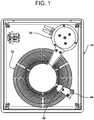
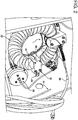
- a case 10 houses elements of the components of a current sensing apparatus. Many of the components of the apparatus are known in the art, and are not illustrated or described in detail herein.
- a light source sends light through a waveguide to a linear polarizer and then to a splitter to create two linearly polarized light waves that are then modulated by the modulator 20.
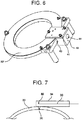
- the light goes out of the modulator 20 through an optical fiber 30 (see Fig. 2 ) in a loop around the current carrying conductor (not shown) after first passing through a quarter waveplate 36 (see Fig. 7 ) that creates right and left hand circularly polarized light from the two linearly polarized light waves.
- the two light waves traverse the fiber 30 loop, reflect off a mirror 50 at the end of the fiber 30 and return around the same path with opposite circular polarization.
- the optical fiber 30 is coiled in the case 10 an integral number of times to form the coil 32.
- the quarter wave plate 36 (shown schematically in Fig. 7 ) is created in a conventional manner by creating a physical structure in the optical fiber 30, and the quarter wave plate is positioned in the coil 32 at the mirror block 40.
- the mirror block 40 is a preferably steel block having a plate 41 and a body 42 that enclose the coil housing 32', which is hollow and through which the fiber 30 extends.
- the body 42 has a channel 43 into which the coil housing 32' is inserted.
- the plate 41 clamps the coil housing 32' in the channel by fasteners inserted through apertures in the plate 41 and are fixed in the body 42.
- the end of the fiber 30 at which the mirror 50 is formed is encased within a protective tube 34, as shown in Figs. 2 and 7 .
- the tube 34 is attached to the outer sheathing of the optical fiber 30, as shown in Fig. 2 , and the fiber 30 "floats" within the tube 34 with space on both sides and the end from the mirror 50, as illustrated schematically in Fig. 7 .
- the tube 34 is inserted into the mirror block 40 through the aperture 44 illustrated in Fig. 6 . Once the tube 34 is inserted in the aperture 44, the position of the mirror 50 relative to the quarter wave plate 36 (see Fig. 7 ) is adjusted. Once the desired position is attained, as described below, the rotary clamp 46 is tightened around the sheathing of the fiber 30 to clamp the fiber 30 and, therefore, the mirror 50 in the desired position.
- the positions of the mirror 50 and the quarter wave plate 36 can be marked, or otherwise detected, for example using x-ray, magnetic resonance imaging (MRI) or other inspection techniques, and mounted as close to one another as possible to reduce the gap therebetween.
- MRI magnetic resonance imaging
- a magnetic test can be performed, such as by passing a strong magnet over any parts of the device that are sensitive to magnetic fields. The system is monitored for accuracy during the movement of the magnet. The mirror in the tube 34 is moved to each of a plurality of different positions in the block, and the magnet is again passed over the region. After the tube 34 has been placed at each possible position in the range, the tube 34 is mounted at that position at which the system shows optimal accuracy while the magnet is passed over the area being tested. Any method of positioning the mirror 50 as close to the quarter wave plate 36 as possible is contemplated in order to obtain a predetermined maximum gap size.
- the accuracy of the current sensing device is improved by minimizing the gap between the mirror 50 and quarter wave plate 36 due to a portion of the magnetic field created by the current carrying conductor being measured passing through this gap.
- the gap is large, a large amount of the magnetic field passes through the gap and does not have an effect, or has less of an effect, on the phase shift in the fiber 30 passing around the conductor. This causes the error detection to be less accurate.
- the gap is small, less of the magnetic field passes through the gap, and therefore becomes a part of the correction of the invention. If the gap could be closed completely, then the measurement should be ideal. However, this is not possible in most practical situations, and therefore a maximum gap size, which is quite small, is permitted.
- the size of the gap is as small as possible, and is preferably infinitesimal. Of course, it is known that there will essentially always be some finite gap size. However, the most benefit obtained is when the gap is less than 0.02 percent of the total length of the fiber, assuming that the fiber and the gap are exposed to essentially the same magnetic field levels. Thus, for a typical fiber in an apparatus with which the invention is used, a gap of 0.0 to 12 millimeters is preferred, a gap of 0.0 to 6 millimeters is more preferred, and a gap of 0.0 to 2 millimeters is most preferred. A gap of about 15 millimeters or greater is not a small enough gap to meet the requirements of the present invention. Thus, it is critical that the gap be smaller than about 15 millimeters for the apparatus used herein.
- the body 42 and the plate 41 are made of magnetic shielding material, in order that they shield the gap from magnetic fields.
- the body 42 and the plate 41 are preferably made of steel, which offers substantial magnetic shielding for low cost in a material that is relatively easily shaped.
- Other materials that are contemplated are low carbon steel, such as 1018, 1020, 1117, 1010, 1006 and pure steel. Of course, other steel compositions can be used.
- higher permeability material can be used, such as nickel (78-80%) iron alloy, such as that sold under the trademarks HYMU80, HIPERNOM, PERMALLOY 80 and MUMETAL.
- Another nickel iron alloy (48-52% nickel) can be used, and is sold under the trademarks CARPENTER HIGH PERMEABILITY "49", ALLOY 48 and MAGNIFIER 50, among others.
- the latter group is considered medium permeability materials.
- suitable materials A person having ordinary skill will be aware of other suitable materials currently in existence, or which may come into existence, that can substitute for the materials described herein.
- the desired magnetic shields preferably have multiple layers of the shielding material with an air gap between each layer.
- the outermost layer is of the highest permeability material
- the inner layer is of the lowest permeability
- a middle layer is of a medium permeability material.
- Material thicknesses have not been optimized, although it is considered advantageous to have steel of between around 0,3175 cm to 0,635 cm (one-eighth to one-quarter of one inch) thick. Of course, other thicknesses are contemplated.
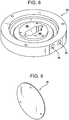
- the modulator 20 is also shielded by the shields 22, 24 and 28, as shown in Figs. 8, 9 and 10 .
- the lower shield 22 mounts to the floor 8 of the case 10, and the middle shield 24 mounts to the lower shield 22.
- the upper shield 28 mounts to the top of the lower shield 22 as shown in Fig. 10 .
- the apertures 25 and 26 permit exit of the fiber 30 as shown in Fig. 2 .
- the entire case 10, including a floor 8 and removable lid (not shown) be made of magnetic shielding material of the types described herein. This provides substantial shielding of the critical components of the apparatus by the very housing of those components. However, this has practical limitations, such as weight and cost that, unless overcome, would limit the ability of such shielding to be implemented.
Landscapes
- Physics & Mathematics (AREA)
- General Physics & Mathematics (AREA)
- Engineering & Computer Science (AREA)
- Power Engineering (AREA)
- Measuring Instrument Details And Bridges, And Automatic Balancing Devices (AREA)
Claims (7)
- Optisches Interferometer umfassend eine optische Faser (30) zum Umlaufen um einen Leiter, um damit einen Weg für einen Lichtstrahl auszubilden, eine Viertel-Wellenplatte (36) in der optischen Faser (30) und einen Spiegel (50) in der Nähe eines Endes der optischen Faser (30) zum Messen eines Stroms durch den Leiter, der auf dem Effekt eines Magnetfeldes basiert, das durch einen durch den Leiter fließenden Strom erzeugt wird, basierend auf Licht, das durch die optische Faser (30) hindurchgeht, ferner umfassend eine Lücke, die zwischen der Viertelwellenplatte (36) und dem Spiegel (50) ausgebildet ist und kleiner als eine vorab festgelegte maximale Lücke ist, um das durch die Lücke hindurchtretende Magnetfeld zu minimieren,
gekennzeichnet durch
eine magnetische Abschirmung (41, 42) um einen wesentlichen Teil des Spalts, um ein durch den Spalt laufendes Magnetfeld weiter zu minimieren, wobei die magnetische Abschirmung (41, 42) umfasst:(a) einen Spiegelblock (40) mit einer Platte (41) und einem Körper (42), der ein hohles Spulengehäuse (32') umgibt, durch das sich die Faser (30) erstreckt, wobei die Faser (30) ein ganzzahliges Vielfach gewickelt ist, um eine Spule (32) zu bilden,(b) wobei besagter Körper (42) einen Kanal (43) aufweist, in den das Spulengehäuse (32') eingesetzt ist, und in besagtem Kanal (43) ein Teil der Faser (30) angeordnet ist, welche die Viertel-Wellenplatte (36) enthält;(c) wobei besagte Platte (41) besagtes Spulengehäuse (32') in dem Kanal (43) durch in die Platte (41) eingesetzte und in dem Körper (42) befestigte Befestigungselemente einklemmt, und(d) eine Öffnung (44), die in dem Spiegelblock (40) ausgebildet ist und sich neben dem Kanal (43) erstreckt, wobei in besagte Öffnung ein Schutzrohr (34) eingesetzt ist, wobei das Rohr (34) das Ende der Faser (30) umhüllt und das Rohr (34) und das Faserende sich durch die Öffnung (44) erstrecken, wodurch das Faserende benachbart zu der Viertel-Wellenplatte (36) angeordnet wird, wobei die Öffnung (44) so konfiguriert ist, dass die Position des Spiegels (50) relativ zur Viertel-Wellenplatte (36) einstellbar ist, und wobei der Spiegelblock (40) eine Drehklemme (46) aufweist, die konfiguriert ist, um um eine Ummantelung der Faser (30) festgezogen zu werden, um die Faser (30) und den Spiegel (50) in einer gewünschten Position festzuklemmen. - Optisches Interferometer nach Anspruch 1, ferner aufweisend eine magnetische Abschirmung (41, 42), die um einen wesentlichen Teil eines Modulators (20) herum ausgebildet ist.
- Optisches Interferometer nach Anspruch 1, ferner aufweisend eine magnetische Abschirmung (41,42), die um einen wesentlichen Teil eines Gehäuses ausgebildet ist, das mindestens den Spalt und einen Modulator (20) und eine Kompensationsspule enthält.
- Optisches Interferometer nach Anspruch 1, wobei ein Zwischenraum wenigstens zwischen dem Schutzrohr (34) und dem Faserende ausgebildet ist.
- Verfahren zum Minimieren von Fehlern in einem optischen Interferometer, umfassend eine optische Faser (30), die sich um einen Leiter erstreckt um damit einen Weg für einen Lichtstrahl auszubilden, eine Viertel-Wellenplatte (36) in der optischen Faser und einen Spiegel (50) in der Nähe eines Endes der optischen Faser (30) zum Messen eines Stroms durch den Leiter, der auf dem Effekt eines Magnetfeldes basiert, das durch einen durch den Leiter fließenden Strom erzeugt wird, basierend auf Licht, das durch die optische Faser (30) hindurchgeht, das Verfahren ferner umfassend die Ausbildung einer Lücke zwischen der Viertel-Wellenplatte (36) und dem Spiegel (50), die kleiner als eine vorab festgelegte maximale Lücke ist, um das durch die Lücke hindurchtretende Magnetfeld zu minimieren, wobei das Verfahren gekennzeichnet ist durch weiteres Minimieren eines durch den Spalt laufenden Magnetfelds durch Bereitstellen einer magnetischen Abschirmung (41, 42) um einen wesentlichen Teil des Spalts, wobei die magnetische Abschirmung (41, 42) umfasst:(a) einen Spiegelblock (40) mit einer Platte (41) und einem Körper (42), der ein hohles Spulengehäuse (32') umgibt, durch das sich die Faser (30) erstreckt, wobei die Faser (30) ein ganzzahliges Vielfach gewickelt ist, um eine Spule (32) zu bilden,(b) wobei besagter Körper (42) einen Kanal (43) aufweist, in den das Spulengehäuse (32') eingesetzt ist, und in besagtem Kanal (43) ein Teil der Faser (30) angeordnet ist, der die Viertel-Wellenplatte (36) enthält;(c) wobei besagte Platte (41) besagtes Spulengehäuse (32') in dem Kanal (43) durch in die Platte (41) eingesetzte und in dem Körper (42) befestigte Befestigungselemente einklemmt, und(d) eine Öffnung (44), die in dem Spiegelblock (40) ausgebildet ist und sich neben dem Kanal (43) erstreckt, wobei in besagte Öffnung ein Schutzrohr (34) eingesetzt ist, wobei das Rohr (34) das Ende der Faser (30) umhüllt und das Rohr (34) und das Faserende sich durch die Öffnung (44) erstrecken, wobei das Faserende benachbart zu der Viertel-Wellenplatte (36) angeordnet wird, wobei die Öffnung (44) so konfiguriert ist, dass die Position des Spiegels (50) relativ zur Viertel-Wellenplatte (36) einstellbar ist, und wobei der Spiegelblock (40) eine Drehklemme (46) aufweist, die konfiguriert ist, um um eine Ummantelung der Faser (30) festgezogen zu werden, um die Faser (30) und den Spiegel (50) in einer gewünschten Position festzuklemmen.
- Verfahren nach Anspruch 5, ferner aufweisend einen Einstellschritt, der aufweist:(a) Bewegen der optischen Faser (30) in eine erste Position;(b) Bestimmen eines Fehlers, wenn sich die optische Faser (30) an der ersten Position befindet;(c) Bewegen der optischen Faser (30) in eine zweite Position;(d) Bestimmen eines Fehlers, wenn sich die optische Faser (30) an der zweiten Position befindet;(e) Vergleichen des Fehlers, wenn sich die optische Faser (30) an der ersten Position befindet, mit dem Fehler, wenn sich die optische Faser (30) an der zweiten Position befindet;(f) Bewegen der optischen Faser (30) in eine Position, die den Fehler weiter minimiert; und dann(g) Fixieren der optischen Faser (30) in Position.
- Verfahren nach Anspruch 5, ferner aufweisend das Festziehen der Drehklemme (46) um eine Ummantelung der Faser, um das Rohr in der gewünschten Position festzuklemmen.
Applications Claiming Priority (2)
| Application Number | Priority Date | Filing Date | Title |
|---|---|---|---|
| US11/874,944 US7602198B2 (en) | 2007-10-19 | 2007-10-19 | Accuracy enhancing mechanism and method for current measuring apparatus |
| PCT/US2008/080110 WO2009052253A1 (en) | 2007-10-19 | 2008-10-16 | Accuracy enhancing mechanism and method for current measuring apparatus |
Publications (3)
| Publication Number | Publication Date |
|---|---|
| EP2201323A1 EP2201323A1 (de) | 2010-06-30 |
| EP2201323A4 EP2201323A4 (de) | 2018-02-21 |
| EP2201323B1 true EP2201323B1 (de) | 2020-04-29 |
Family
ID=40562835
Family Applications (1)
| Application Number | Title | Priority Date | Filing Date |
|---|---|---|---|
| EP08838669.3A Active EP2201323B1 (de) | 2007-10-19 | 2008-10-16 | Präzisionserhöhungsmechanismus und -verfahren für ein faser-optisches Strommessgerät |
Country Status (3)
| Country | Link |
|---|---|
| US (1) | US7602198B2 (de) |
| EP (1) | EP2201323B1 (de) |
| WO (1) | WO2009052253A1 (de) |
Families Citing this family (2)
| Publication number | Priority date | Publication date | Assignee | Title |
|---|---|---|---|---|
| RU2677990C2 (ru) | 2014-08-19 | 2019-01-22 | Абб Швайц Аг | Оптический датчик с двулучепреломляющим измерительным spun-волокном |
| CN109581024B (zh) * | 2017-09-29 | 2020-12-18 | 南京南瑞继保电气有限公司 | 一种光纤电流互感器 |
Family Cites Families (16)
| Publication number | Priority date | Publication date | Assignee | Title |
|---|---|---|---|---|
| US4491795A (en) | 1982-05-17 | 1985-01-01 | Honeywell Inc. | Josephson junction interferometer device for detection of curl-free magnetic vector potential fields |
| FR2632404B1 (fr) * | 1988-06-03 | 1990-09-21 | Elf Aquitaine | Capteur interferometrique et son utilisation dans un dispositif interferometrique |
| US5677622A (en) | 1991-12-24 | 1997-10-14 | The University Of Sydney | Current sensor using a Sagnac interferometer and spun, single mode birefringent optical fiber to detect current via the Faraday effect |
| US5715080A (en) | 1992-09-11 | 1998-02-03 | Scerbak; David G. | Compact uniform field Faraday isolator |
| US5521774A (en) | 1994-03-18 | 1996-05-28 | Cartesian Data, Inc. | Memory storage module for storing and accessing |
| US5694216A (en) * | 1996-04-25 | 1997-12-02 | University Of Central Florida | Scanning heterodyne acousto-optical interferometers |
| JP3488576B2 (ja) * | 1996-08-30 | 2004-01-19 | 株式会社東芝 | 光変流器 |
| US6915048B2 (en) * | 2001-06-18 | 2005-07-05 | Cidra Corporation | Fabry-perot filter/resonator |
| JP3933965B2 (ja) * | 2002-03-14 | 2007-06-20 | 富士通株式会社 | 波長特性可変装置、光増幅器および光伝送システム |
| US6886365B2 (en) * | 2002-11-04 | 2005-05-03 | Harris Corporation | Fiber optic Fabry-Perot interferometer and associated methods |
| US6943892B2 (en) | 2003-01-29 | 2005-09-13 | Sarnoff Corporation | Instrument having a multi-mode optical element and method |
| ATE377195T1 (de) * | 2003-09-03 | 2007-11-15 | Abb Research Ltd | Temperaturstabilisierte sensorspule und stromsensor |
| EP1586854A3 (de) * | 2004-04-15 | 2006-02-08 | Davidson Instruments | Interferometrischer Signalkonditionierer zur Messung der absoluten Länge von Spalten in einem fiberoptischen Fabry-Pérot-Interferometer |
| US7599069B2 (en) * | 2005-05-06 | 2009-10-06 | The University Of Chicago | Vector beam generator using a passively phase stable optical interferometer |
| WO2007112600A1 (en) * | 2006-04-04 | 2007-10-11 | Abb Research Ltd | Fiber-optic current sensor with sum detection |
| US8115937B2 (en) * | 2006-08-16 | 2012-02-14 | Davidson Instruments | Methods and apparatus for measuring multiple Fabry-Perot gaps |
-
2007
- 2007-10-19 US US11/874,944 patent/US7602198B2/en active Active
-
2008
- 2008-10-16 WO PCT/US2008/080110 patent/WO2009052253A1/en not_active Ceased
- 2008-10-16 EP EP08838669.3A patent/EP2201323B1/de active Active
Non-Patent Citations (1)
| Title |
|---|
| None * |
Also Published As
| Publication number | Publication date |
|---|---|
| EP2201323A4 (de) | 2018-02-21 |
| US7602198B2 (en) | 2009-10-13 |
| US20090102454A1 (en) | 2009-04-23 |
| WO2009052253A1 (en) | 2009-04-23 |
| EP2201323A1 (de) | 2010-06-30 |
Similar Documents
| Publication | Publication Date | Title |
|---|---|---|
| EP2304447B1 (de) | Magnetoresistive sensor-anordnung zur strommessung | |
| US8320719B2 (en) | Method for manufacturing a fiber optic current sensor with inherent temperature compensation of the faraday effect | |
| KR100248128B1 (ko) | 광변류기 | |
| RU2677990C2 (ru) | Оптический датчик с двулучепреломляющим измерительным spun-волокном | |
| EP0853765A1 (de) | Stromfühler mit kompensation für die temperaturabhängigkeit der verdet-konstante | |
| US8461822B2 (en) | Temperature compensated fiber optic current or magnetic field sensor with insensitivity to variations in sensor parameters | |
| US5237265A (en) | Fiber optics arrangement for measuring the intensity of an electric current | |
| Bohnert et al. | Fiber-optic dc current sensor for the electro-winning industry | |
| CN112034229A (zh) | 一种全光纤电压互感器 | |
| EP2201323B1 (de) | Präzisionserhöhungsmechanismus und -verfahren für ein faser-optisches Strommessgerät | |
| CA2258602A1 (en) | Fiber optic current sensor with bend birefringence compensation | |
| Mali et al. | Design methodologies for measurement of KA DC current: A review | |
| Liehr | Optical measurement of currents in power converters | |
| JP2000111586A (ja) | 電流計測装置 | |
| Song et al. | A faraday effect based clamp-on magneto-optical current transducer for power systems | |
| JP4215313B2 (ja) | 光変流器 | |
| Silventoinen et al. | Review on the current measurement systems in power electronics | |
| US8933686B2 (en) | Single-phase optical current transformer | |
| JP2002107386A (ja) | 電流センサ | |
| Fan et al. | Electromagnetic Sensors | |
| Lovchy | Simulation of the sensitivity of a fiber-optic magneto-optical electric current sensor with a strictly nonuniform distribution of the magnetic field around the loop | |
| Song et al. | A clamp-on magneto-optical current transducer for power systems | |
| Lim et al. | Hybrid fiber-optic current sensor using two Faraday glass-slab magnetic field sensors | |
| JP2002277491A (ja) | 電流センサ | |
| Yoshino et al. | Optical Current Sensors |
Legal Events
| Date | Code | Title | Description |
|---|---|---|---|
| PUAI | Public reference made under article 153(3) epc to a published international application that has entered the european phase |
Free format text: ORIGINAL CODE: 0009012 |
|
| 17P | Request for examination filed |
Effective date: 20100511 |
|
| AK | Designated contracting states |
Kind code of ref document: A1 Designated state(s): AT BE BG CH CY CZ DE DK EE ES FI FR GB GR HR HU IE IS IT LI LT LU LV MC MT NL NO PL PT RO SE SI SK TR |
|
| AX | Request for extension of the european patent |
Extension state: AL BA MK RS |
|
| DAX | Request for extension of the european patent (deleted) | ||
| RIN1 | Information on inventor provided before grant (corrected) |
Inventor name: SHERMAN, CHRISTOPHER, S. Inventor name: MASRI, FARID, E. |
|
| RA4 | Supplementary search report drawn up and despatched (corrected) |
Effective date: 20180124 |
|
| RIC1 | Information provided on ipc code assigned before grant |
Ipc: G01R 15/24 20060101ALI20180118BHEP Ipc: G01B 9/02 20060101AFI20180118BHEP |
|
| STAA | Information on the status of an ep patent application or granted ep patent |
Free format text: STATUS: EXAMINATION IS IN PROGRESS |
|
| 17Q | First examination report despatched |
Effective date: 20181205 |
|
| REG | Reference to a national code |
Ref country code: DE Ref legal event code: R079 Ref document number: 602008062604 Country of ref document: DE Free format text: PREVIOUS MAIN CLASS: G01B0009020000 Ipc: G01R0015240000 |
|
| GRAP | Despatch of communication of intention to grant a patent |
Free format text: ORIGINAL CODE: EPIDOSNIGR1 |
|
| STAA | Information on the status of an ep patent application or granted ep patent |
Free format text: STATUS: GRANT OF PATENT IS INTENDED |
|
| RIC1 | Information provided on ipc code assigned before grant |
Ipc: G01R 15/24 20060101AFI20191010BHEP |
|
| INTG | Intention to grant announced |
Effective date: 20191112 |
|
| GRAS | Grant fee paid |
Free format text: ORIGINAL CODE: EPIDOSNIGR3 |
|
| GRAJ | Information related to disapproval of communication of intention to grant by the applicant or resumption of examination proceedings by the epo deleted |
Free format text: ORIGINAL CODE: EPIDOSDIGR1 |
|
| GRAL | Information related to payment of fee for publishing/printing deleted |
Free format text: ORIGINAL CODE: EPIDOSDIGR3 |
|
| STAA | Information on the status of an ep patent application or granted ep patent |
Free format text: STATUS: EXAMINATION IS IN PROGRESS |
|
| GRAR | Information related to intention to grant a patent recorded |
Free format text: ORIGINAL CODE: EPIDOSNIGR71 |
|
| STAA | Information on the status of an ep patent application or granted ep patent |
Free format text: STATUS: GRANT OF PATENT IS INTENDED |
|
| GRAA | (expected) grant |
Free format text: ORIGINAL CODE: 0009210 |
|
| STAA | Information on the status of an ep patent application or granted ep patent |
Free format text: STATUS: THE PATENT HAS BEEN GRANTED |
|
| INTC | Intention to grant announced (deleted) | ||
| AK | Designated contracting states |
Kind code of ref document: B1 Designated state(s): AT BE BG CH CY CZ DE DK EE ES FI FR GB GR HR HU IE IS IT LI LT LU LV MC MT NL NO PL PT RO SE SI SK TR |
|
| INTG | Intention to grant announced |
Effective date: 20200324 |
|
| REG | Reference to a national code |
Ref country code: GB Ref legal event code: FG4D |
|
| REG | Reference to a national code |
Ref country code: CH Ref legal event code: EP |
|
| REG | Reference to a national code |
Ref country code: DE Ref legal event code: R096 Ref document number: 602008062604 Country of ref document: DE |
|
| REG | Reference to a national code |
Ref country code: AT Ref legal event code: REF Ref document number: 1264120 Country of ref document: AT Kind code of ref document: T Effective date: 20200515 |
|
| REG | Reference to a national code |
Ref country code: IE Ref legal event code: FG4D |
|
| REG | Reference to a national code |
Ref country code: CH Ref legal event code: NV Representative=s name: SCHNEIDER FELDMANN AG PATENT- UND MARKENANWAEL, CH |
|
| REG | Reference to a national code |
Ref country code: NL Ref legal event code: MP Effective date: 20200429 |
|
| REG | Reference to a national code |
Ref country code: LT Ref legal event code: MG4D |
|
| REG | Reference to a national code |
Ref country code: CH Ref legal event code: PFA Owner name: DYNAMP LLC, US Free format text: FORMER OWNER: DYNAMP LLC, US |
|
| PG25 | Lapsed in a contracting state [announced via postgrant information from national office to epo] |
Ref country code: GR Free format text: LAPSE BECAUSE OF FAILURE TO SUBMIT A TRANSLATION OF THE DESCRIPTION OR TO PAY THE FEE WITHIN THE PRESCRIBED TIME-LIMIT Effective date: 20200730 Ref country code: IS Free format text: LAPSE BECAUSE OF FAILURE TO SUBMIT A TRANSLATION OF THE DESCRIPTION OR TO PAY THE FEE WITHIN THE PRESCRIBED TIME-LIMIT Effective date: 20200829 Ref country code: PT Free format text: LAPSE BECAUSE OF FAILURE TO SUBMIT A TRANSLATION OF THE DESCRIPTION OR TO PAY THE FEE WITHIN THE PRESCRIBED TIME-LIMIT Effective date: 20200831 Ref country code: SE Free format text: LAPSE BECAUSE OF FAILURE TO SUBMIT A TRANSLATION OF THE DESCRIPTION OR TO PAY THE FEE WITHIN THE PRESCRIBED TIME-LIMIT Effective date: 20200429 Ref country code: NO Free format text: LAPSE BECAUSE OF FAILURE TO SUBMIT A TRANSLATION OF THE DESCRIPTION OR TO PAY THE FEE WITHIN THE PRESCRIBED TIME-LIMIT Effective date: 20200729 Ref country code: FI Free format text: LAPSE BECAUSE OF FAILURE TO SUBMIT A TRANSLATION OF THE DESCRIPTION OR TO PAY THE FEE WITHIN THE PRESCRIBED TIME-LIMIT Effective date: 20200429 Ref country code: LT Free format text: LAPSE BECAUSE OF FAILURE TO SUBMIT A TRANSLATION OF THE DESCRIPTION OR TO PAY THE FEE WITHIN THE PRESCRIBED TIME-LIMIT Effective date: 20200429 |
|
| REG | Reference to a national code |
Ref country code: AT Ref legal event code: MK05 Ref document number: 1264120 Country of ref document: AT Kind code of ref document: T Effective date: 20200429 |
|
| PG25 | Lapsed in a contracting state [announced via postgrant information from national office to epo] |
Ref country code: LV Free format text: LAPSE BECAUSE OF FAILURE TO SUBMIT A TRANSLATION OF THE DESCRIPTION OR TO PAY THE FEE WITHIN THE PRESCRIBED TIME-LIMIT Effective date: 20200429 Ref country code: BG Free format text: LAPSE BECAUSE OF FAILURE TO SUBMIT A TRANSLATION OF THE DESCRIPTION OR TO PAY THE FEE WITHIN THE PRESCRIBED TIME-LIMIT Effective date: 20200729 Ref country code: HR Free format text: LAPSE BECAUSE OF FAILURE TO SUBMIT A TRANSLATION OF THE DESCRIPTION OR TO PAY THE FEE WITHIN THE PRESCRIBED TIME-LIMIT Effective date: 20200429 |
|
| PG25 | Lapsed in a contracting state [announced via postgrant information from national office to epo] |
Ref country code: NL Free format text: LAPSE BECAUSE OF FAILURE TO SUBMIT A TRANSLATION OF THE DESCRIPTION OR TO PAY THE FEE WITHIN THE PRESCRIBED TIME-LIMIT Effective date: 20200429 |
|
| PG25 | Lapsed in a contracting state [announced via postgrant information from national office to epo] |
Ref country code: EE Free format text: LAPSE BECAUSE OF FAILURE TO SUBMIT A TRANSLATION OF THE DESCRIPTION OR TO PAY THE FEE WITHIN THE PRESCRIBED TIME-LIMIT Effective date: 20200429 Ref country code: IT Free format text: LAPSE BECAUSE OF FAILURE TO SUBMIT A TRANSLATION OF THE DESCRIPTION OR TO PAY THE FEE WITHIN THE PRESCRIBED TIME-LIMIT Effective date: 20200429 Ref country code: DK Free format text: LAPSE BECAUSE OF FAILURE TO SUBMIT A TRANSLATION OF THE DESCRIPTION OR TO PAY THE FEE WITHIN THE PRESCRIBED TIME-LIMIT Effective date: 20200429 Ref country code: ES Free format text: LAPSE BECAUSE OF FAILURE TO SUBMIT A TRANSLATION OF THE DESCRIPTION OR TO PAY THE FEE WITHIN THE PRESCRIBED TIME-LIMIT Effective date: 20200429 Ref country code: AT Free format text: LAPSE BECAUSE OF FAILURE TO SUBMIT A TRANSLATION OF THE DESCRIPTION OR TO PAY THE FEE WITHIN THE PRESCRIBED TIME-LIMIT Effective date: 20200429 Ref country code: CZ Free format text: LAPSE BECAUSE OF FAILURE TO SUBMIT A TRANSLATION OF THE DESCRIPTION OR TO PAY THE FEE WITHIN THE PRESCRIBED TIME-LIMIT Effective date: 20200429 Ref country code: RO Free format text: LAPSE BECAUSE OF FAILURE TO SUBMIT A TRANSLATION OF THE DESCRIPTION OR TO PAY THE FEE WITHIN THE PRESCRIBED TIME-LIMIT Effective date: 20200429 |
|
| REG | Reference to a national code |
Ref country code: DE Ref legal event code: R097 Ref document number: 602008062604 Country of ref document: DE |
|
| PG25 | Lapsed in a contracting state [announced via postgrant information from national office to epo] |
Ref country code: SK Free format text: LAPSE BECAUSE OF FAILURE TO SUBMIT A TRANSLATION OF THE DESCRIPTION OR TO PAY THE FEE WITHIN THE PRESCRIBED TIME-LIMIT Effective date: 20200429 Ref country code: PL Free format text: LAPSE BECAUSE OF FAILURE TO SUBMIT A TRANSLATION OF THE DESCRIPTION OR TO PAY THE FEE WITHIN THE PRESCRIBED TIME-LIMIT Effective date: 20200429 |
|
| PLBE | No opposition filed within time limit |
Free format text: ORIGINAL CODE: 0009261 |
|
| STAA | Information on the status of an ep patent application or granted ep patent |
Free format text: STATUS: NO OPPOSITION FILED WITHIN TIME LIMIT |
|
| 26N | No opposition filed |
Effective date: 20210201 |
|
| PG25 | Lapsed in a contracting state [announced via postgrant information from national office to epo] |
Ref country code: SI Free format text: LAPSE BECAUSE OF FAILURE TO SUBMIT A TRANSLATION OF THE DESCRIPTION OR TO PAY THE FEE WITHIN THE PRESCRIBED TIME-LIMIT Effective date: 20200429 |
|
| GBPC | Gb: european patent ceased through non-payment of renewal fee |
Effective date: 20201016 |
|
| PG25 | Lapsed in a contracting state [announced via postgrant information from national office to epo] |
Ref country code: MC Free format text: LAPSE BECAUSE OF FAILURE TO SUBMIT A TRANSLATION OF THE DESCRIPTION OR TO PAY THE FEE WITHIN THE PRESCRIBED TIME-LIMIT Effective date: 20200429 Ref country code: LU Free format text: LAPSE BECAUSE OF NON-PAYMENT OF DUE FEES Effective date: 20201016 |
|
| REG | Reference to a national code |
Ref country code: BE Ref legal event code: MM Effective date: 20201031 |
|
| PG25 | Lapsed in a contracting state [announced via postgrant information from national office to epo] |
Ref country code: BE Free format text: LAPSE BECAUSE OF NON-PAYMENT OF DUE FEES Effective date: 20201031 Ref country code: GB Free format text: LAPSE BECAUSE OF NON-PAYMENT OF DUE FEES Effective date: 20201016 |
|
| PG25 | Lapsed in a contracting state [announced via postgrant information from national office to epo] |
Ref country code: IE Free format text: LAPSE BECAUSE OF NON-PAYMENT OF DUE FEES Effective date: 20201016 |
|
| PG25 | Lapsed in a contracting state [announced via postgrant information from national office to epo] |
Ref country code: TR Free format text: LAPSE BECAUSE OF FAILURE TO SUBMIT A TRANSLATION OF THE DESCRIPTION OR TO PAY THE FEE WITHIN THE PRESCRIBED TIME-LIMIT Effective date: 20200429 Ref country code: MT Free format text: LAPSE BECAUSE OF FAILURE TO SUBMIT A TRANSLATION OF THE DESCRIPTION OR TO PAY THE FEE WITHIN THE PRESCRIBED TIME-LIMIT Effective date: 20200429 Ref country code: CY Free format text: LAPSE BECAUSE OF FAILURE TO SUBMIT A TRANSLATION OF THE DESCRIPTION OR TO PAY THE FEE WITHIN THE PRESCRIBED TIME-LIMIT Effective date: 20200429 |
|
| REG | Reference to a national code |
Ref country code: CH Ref legal event code: U11 Free format text: ST27 STATUS EVENT CODE: U-0-0-U10-U11 (AS PROVIDED BY THE NATIONAL OFFICE) Effective date: 20251101 |
|
| PGFP | Annual fee paid to national office [announced via postgrant information from national office to epo] |
Ref country code: FR Payment date: 20251024 Year of fee payment: 18 |
|
| PGFP | Annual fee paid to national office [announced via postgrant information from national office to epo] |
Ref country code: CH Payment date: 20251101 Year of fee payment: 18 |
|
| PGFP | Annual fee paid to national office [announced via postgrant information from national office to epo] |
Ref country code: DE Payment date: 20251222 Year of fee payment: 18 |