EP2201602B1 - Éléments d'alignement pour communication de proximité - Google Patents
Éléments d'alignement pour communication de proximité Download PDFInfo
- Publication number
- EP2201602B1 EP2201602B1 EP08799569.2A EP08799569A EP2201602B1 EP 2201602 B1 EP2201602 B1 EP 2201602B1 EP 08799569 A EP08799569 A EP 08799569A EP 2201602 B1 EP2201602 B1 EP 2201602B1
- Authority
- EP
- European Patent Office
- Prior art keywords
- semiconductor die
- semiconductor
- feature
- proximity
- positive
- Prior art date
- Legal status (The legal status is an assumption and is not a legal conclusion. Google has not performed a legal analysis and makes no representation as to the accuracy of the status listed.)
- Active
Links
Images






Classifications
-
- H—ELECTRICITY
- H10—SEMICONDUCTOR DEVICES; ELECTRIC SOLID-STATE DEVICES NOT OTHERWISE PROVIDED FOR
- H10D—INORGANIC ELECTRIC SEMICONDUCTOR DEVICES
- H10D62/00—Semiconductor bodies, or regions thereof, of devices having potential barriers
- H10D62/10—Shapes, relative sizes or dispositions of the regions of the semiconductor bodies; Shapes of the semiconductor bodies
- H10D62/117—Shapes of semiconductor bodies
-
- H—ELECTRICITY
- H10—SEMICONDUCTOR DEVICES; ELECTRIC SOLID-STATE DEVICES NOT OTHERWISE PROVIDED FOR
- H10W—GENERIC PACKAGES, INTERCONNECTIONS, CONNECTORS OR OTHER CONSTRUCTIONAL DETAILS OF DEVICES COVERED BY CLASS H10
- H10W46/00—Marks applied to devices, e.g. for alignment or identification
-
- H—ELECTRICITY
- H10—SEMICONDUCTOR DEVICES; ELECTRIC SOLID-STATE DEVICES NOT OTHERWISE PROVIDED FOR
- H10W—GENERIC PACKAGES, INTERCONNECTIONS, CONNECTORS OR OTHER CONSTRUCTIONAL DETAILS OF DEVICES COVERED BY CLASS H10
- H10W72/00—Interconnections or connectors in packages
-
- H—ELECTRICITY
- H10—SEMICONDUCTOR DEVICES; ELECTRIC SOLID-STATE DEVICES NOT OTHERWISE PROVIDED FOR
- H10W—GENERIC PACKAGES, INTERCONNECTIONS, CONNECTORS OR OTHER CONSTRUCTIONAL DETAILS OF DEVICES COVERED BY CLASS H10
- H10W90/00—Package configurations
-
- H—ELECTRICITY
- H10—SEMICONDUCTOR DEVICES; ELECTRIC SOLID-STATE DEVICES NOT OTHERWISE PROVIDED FOR
- H10W—GENERIC PACKAGES, INTERCONNECTIONS, CONNECTORS OR OTHER CONSTRUCTIONAL DETAILS OF DEVICES COVERED BY CLASS H10
- H10W46/00—Marks applied to devices, e.g. for alignment or identification
- H10W46/101—Marks applied to devices, e.g. for alignment or identification characterised by the type of information, e.g. logos or symbols
-
- H—ELECTRICITY
- H10—SEMICONDUCTOR DEVICES; ELECTRIC SOLID-STATE DEVICES NOT OTHERWISE PROVIDED FOR
- H10W—GENERIC PACKAGES, INTERCONNECTIONS, CONNECTORS OR OTHER CONSTRUCTIONAL DETAILS OF DEVICES COVERED BY CLASS H10
- H10W46/00—Marks applied to devices, e.g. for alignment or identification
- H10W46/301—Marks applied to devices, e.g. for alignment or identification for alignment
-
- H—ELECTRICITY
- H10—SEMICONDUCTOR DEVICES; ELECTRIC SOLID-STATE DEVICES NOT OTHERWISE PROVIDED FOR
- H10W—GENERIC PACKAGES, INTERCONNECTIONS, CONNECTORS OR OTHER CONSTRUCTIONAL DETAILS OF DEVICES COVERED BY CLASS H10
- H10W46/00—Marks applied to devices, e.g. for alignment or identification
- H10W46/601—Marks applied to devices, e.g. for alignment or identification for use after dicing
- H10W46/603—Formed on wafers or substrates before dicing and remaining on chips after dicing
-
- H—ELECTRICITY
- H10—SEMICONDUCTOR DEVICES; ELECTRIC SOLID-STATE DEVICES NOT OTHERWISE PROVIDED FOR
- H10W—GENERIC PACKAGES, INTERCONNECTIONS, CONNECTORS OR OTHER CONSTRUCTIONAL DETAILS OF DEVICES COVERED BY CLASS H10
- H10W90/00—Package configurations
- H10W90/20—Configurations of stacked chips
- H10W90/293—Configurations of stacked chips characterised by non-galvanic coupling between the chips, e.g. capacitive coupling
-
- H—ELECTRICITY
- H10—SEMICONDUCTOR DEVICES; ELECTRIC SOLID-STATE DEVICES NOT OTHERWISE PROVIDED FOR
- H10W—GENERIC PACKAGES, INTERCONNECTIONS, CONNECTORS OR OTHER CONSTRUCTIONAL DETAILS OF DEVICES COVERED BY CLASS H10
- H10W90/00—Package configurations
- H10W90/20—Configurations of stacked chips
- H10W90/293—Configurations of stacked chips characterised by non-galvanic coupling between the chips, e.g. capacitive coupling
- H10W90/295—Configurations of stacked chips characterised by non-galvanic coupling between the chips, e.g. capacitive coupling optical coupling
-
- H—ELECTRICITY
- H10—SEMICONDUCTOR DEVICES; ELECTRIC SOLID-STATE DEVICES NOT OTHERWISE PROVIDED FOR
- H10W—GENERIC PACKAGES, INTERCONNECTIONS, CONNECTORS OR OTHER CONSTRUCTIONAL DETAILS OF DEVICES COVERED BY CLASS H10
- H10W90/00—Package configurations
- H10W90/701—Package configurations characterised by the relative positions of pads or connectors relative to package parts
- H10W90/721—Package configurations characterised by the relative positions of pads or connectors relative to package parts of bump connectors
- H10W90/722—Package configurations characterised by the relative positions of pads or connectors relative to package parts of bump connectors between stacked chips
Definitions
- the present invention relates to techniques for aligning semiconductor dies. More specifically, the present invention relates to facilitating proximity communication by aligning proximity connectors on adjacent semiconductor dies.
- One promising technique involves integrating arrays of capacitive transmitters and receivers onto semiconductor chips to facilitate inter-chip communication. If a first chip is situated face-to-face with a second chip so that transmitter pads on the first chip are capacitively coupled with receiver pads on the second chip, the first chip can directly transmit signals to the second chip without having to route the signals through intervening signal lines within a printed circuit board.
- Capacitive coupling requires precise alignment between the transmitter pads and the receiver pads (both of which are more generally referred to as proximity connectors), both in a plane defined by the pads and in a direction perpendicular to the plane. Misalignment between the transmitter pads and the receiver pads may cause each receiving pad to span two transmitting pads, thereby destroying a received signal. In theory, for communication to be possible chips must be aligned so that misalignment is less than half of a pitch between the pads. In practice, the alignment requirements may be more stringent. In addition, reducing misalignment can improve communication performance between the chips and reduce power consumption.
- FIG. 1 illustrates one such approach in which negative features, such as etch pits 112, and micro-spheres 114 are used to align semiconductor dies 110 (and thus proximity connectors) in a multi-chip module ( MCM ).
- MCM multi-chip module
- etch-pits can be defined photolithographically using a subtractive process (i.e., a photolithographic process that removes material) before, during, or after circuit fabrication on the semiconductor dies 110. This enables the etch pits 112 to be accurately placed on the semiconductor dies 110 in relationship to circuits and the proximity connectors. Therefore, the photolithographic alignment between the etch pits 112 and circuits establishes precise alignment between circuits on the top and bottom semiconductor dies 110.
- the alignment in the X , Y , and Z directions, as well as the angular alignment between semiconductor dies 110 depends only on the relative sizes of the etch-pits 112 and the micro-spheres 114, and on the orientation and placement of the etch pits 112 on the semiconductor dies 110.
- the lateral alignment between circuits on the semiconductor dies 110 is achieved in a 'snap-fit' manner, provided the micro-spheres 114 are appropriately sized to fit into the etched pits 112.
- micro-spheres 114 that are too large do not fit into the etch pits 112, and micro-spheres 114 that are too small do not properly align the top and bottom semiconductor dies 110.
- micro-spheres 114 sit in the groove of the etch pits 112 correctly (for example, their equators lie exactly at or higher than the surface of the semiconductor die 110-1 and exactly at or lower than the surface of semiconductor die 110-2) then circuits on the top and bottom semiconductor dies 110 are precisely aligned.
- alignment in the Z direction is a function of the photolithographic feature size of the etch pits 112, the etch depth of the etch pits 112, and the diameter of the micro-spheres 114.
- EP 1,650,801 describes a method and apparatus providing capacitive communication between opposed communication pads on first and second chips. Alignment spurs provide positive alignment of communication pads.
- US 6,495,396 describes a multi-chip semiconductor that comprises a first and second semiconductor devices.
- the first semiconductor device has a first surface containing a first ridge alignment member and a second ridge alignment member with a receiving area between the first and second ridge alignment members.
- the second semiconductor device has a second surface containing a third ridge alignment member, the second semiconductor device being positioned such that at least a portion of the third ridge alignment member is located within the receiving area of the first semiconductor device.
- Embodiments of a semiconductor die, an MCM, and systems that include the features disclosed herein. MCM are described.
- the MCM which is sometimes referred to as a macro-chip, includes an array of chip modules (CMs) or single-chip modules ( SCMs ), and a given SCM includes at least one semiconductor die.
- the semiconductor die communicates with other semiconductor dies, SCMs , and/or devices in the MCM using proximity communication of electrical (capacitively coupled) signals and/or proximity communication of optical signals (which are, respectively, sometimes referred to as electrical proximity communication and optical proximity communication). This proximity communication occurs via proximity pads or connectors that are located on or are proximate to a surface of the semiconductor die.
- a given semiconductor die may include positive features (which protrude or extend above a surrounding region) that are photolithographically defined using an additive (i.e., a material-deposition) and/or a subtractive (i.e., a material-removal) processes. These positive features may include: hemispheres, bumps or top-hat shapes, ridges, pyramids, and/or truncated pyramids. In some embodiments, positive features on a first semiconductor die mate with or couple to negative features (which is positioned below or recessed relative to a surrounding region) on a second semiconductor die.
- positive and/or negative features are used in combination with micro-spheres or balls.
- the micro-spheres may be used to couple power or optical signals to the semiconductor die, as well as providing the necessary alignment between the semiconductor dies. Note that this approach to aligning proximity connectors can be implemented in a wafer-scale process, thereby facilitating simpler and lower cost assembly of MCMs.
- Embodiments of the semiconductor die may be used in a variety of applications, including: telephony, storage area networks, data centers, networks (such as local area networks), and/or computer systems (such as multi-processor computer systems).
- the semiconductor die may be included in a switch in a backplane that is coupled to multiple processor blades, or in a switch that is coupled to different types of components (such as processors, memory, I/O devices, and/or peripheral devices).
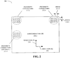
- FIG 2 presents a block diagram illustrating an embodiment of a device 200 that includes proximity connectors 212 (which may be capacitive, optical, inductive, and/or conductive-based connectors).
- Device 200 may include at least one semiconductor die 210, where semiconductor die 210 may include integrated circuit electronics corresponding to layers deposited on a semiconductor substrate.
- semiconductor die 210 may be packaged in an SCM and/or an MCM , where the MCM may include two or more SCMs. When packaged, for example in the SCM or the MCM , semiconductor die 210 is sometimes referred to as a "chip.”
- the proximity connectors 212 may be located on or proximate to at least one surface of the semiconductor die 210, the SCM and/or the MCM. In other embodiments, the semiconductor die 210, the SCM and/or the MCM may be coupled to the proximity connectors 212. In an exemplary embodiment, the proximity connectors 212 are substantially located at or near one or more corners (proximity connectors 212-1 and 212-2) and/or edges (proximity connectors 212-3) of the semiconductor die 210. In other embodiments, proximity connectors 212 may be situated at one or more arbitrary locations on, or proximate to, the surface of the semiconductor die 210.
- first pitch 214-1 between adjacent connectors or pads in a first direction ( X ) 216 of the surface and a second pitch 214-2 between adjacent connectors or pads in a second direction ( Y ) 218 of the surface.
- first pitch 214-1 and the second pitch 214-2 are approximately equal.
- FIG. 3 presents a block diagram illustrating an embodiment of an MCM 300 that includes semiconductor dies 210 that communicate using capacitively coupled proximity communication (which is used as an illustration).
- Semiconductor dies 210 may include proximity connectors or pads 212 that are located on or proximate to at least surfaces 308 of the semiconductor dies 210.
- the proximity connectors 212 may be situated beneath protective layers such that they are located below the surfaces 308.
- subsets of the proximity connectors 212 may be coupled to transmit circuits 310 (such as transmit drivers) and receive circuits 312 (such as receivers).
- One of the transmit circuits 310, at least a subset of the proximity connectors 212 on the adjacent semiconductor dies 210, and one of the receive circuits 312 may constitute a communication channel.
- the communication channel may include transmit circuit 310-1, some of the proximity connectors 212, and receive circuit 312-1.
- transmit circuits 310 and receive circuits 312 may utilize voltage-mode signaling (i.e., voltage-mode drivers and receivers).
- semiconductor dies 210 may also include wiring and electronics (not shown) to relay the data signals to additional electronics on the semiconductor dies 210, such as logic, memory (for example, a packet buffer memory), I/O ports, demultiplexers, multiplexers, and switching elements.
- transmit and receive proximity connectors 212 on adjacent semiconductor dies 210 may have, at worst, only limited misalignment, i.e., substantially accurate alignment.
- the alignment between two or more proximity connectors 212 on adjacent semiconductor dies 210 may be within a few microns in the first direction ( X ) 216 ( FIG. 2 ) and/or a few microns in the second direction ( Y ) 218 ( FIG.
- MCM 300 illustrates a misalignment 314 in the third direction ( Z ).
- the proximity connectors 212 may be aligned in six degrees of freedom, including: the first direction ( X ) 216 ( FIG. 2 ); the second direction ( Y ) 218 ( FIG. 2 ); the third direction ( Z ); an angle in the first plane defined by the first direction ( X ) 216 ( FIG. 2 ) and the second direction ( Y ) 218 ( FIG. 2 ); an angle in a second plane defined by the first direction ( X ) 216 ( FIG. 2 ) and the third direction ( Z ); and an angle in a third plane defined by the second direction ( Y ) 218 ( FIG. 2 ) and the third direction ( Z).
- X 216, Y 218, and Z are the normal orthogonal axes of 3-space. Also note that if a surface, such as the surface 308-1, of either of the adjacent semiconductor dies 210 is non-planar (for example, due to quadrapole distortion), additional alignment problems may be introduced.
- allowed misalignment in the first direction ( X ) 216 ( FIG. 2 ), the second direction ( Y ) 218 ( FIG. 2 ) and/or the third direction ( Z ) is less than one half of the pitch 214 ( FIG. 2 ) between adjacent pads 212.
- misalignment in the first direction ( X ) 216 ( FIG. 2 ) and/or the second direction ( Y ) 218 ( FIG. 2 ) may be less than 25 ⁇ m
- the misalignment 314 in the third direction ( Z ) may be less than 5 ⁇ m.
- the misalignment 314 is between 1 and 10 ⁇ m.
- Solutions such as self-alignment and/or self-adjustment of relative positions of the proximity connectors 212 on adjacent semiconductor dies 210 and/or in a component (such as a bridge chip) coupling two or more semiconductor dies 210, may reduce and/or eliminate the misalignment 314 in the third direction ( Z ).
- structures that have flexibility compliance or are spring like may be used.
- a feedback control loop may be used to reduce and/or eliminate the misalignment 314 in the third direction ( Z ).
- alignment of the semiconductor dies 210 (and thus, at least some of the proximity connectors 212) may be facilitated by coupling of alignment features 316 on or proximate to the surfaces 308.
- Reducing or eliminating the misalignment 314, in turn, may lead to at least partial overlap of one or more proximity connectors 212 on the adjacent semiconductor dies 210 and increase a magnitude of the capacitively coupled data signals.
- the solutions may reduce misalignment in the first plane, i.e., the plane including at least some of the proximity connectors 212, when used in conjunction with techniques such as electronic steering (where data signals are routed to given proximity connectors 212 based on the alignment in the first plane). Consequently, these solutions may facilitate proximity communication between the semiconductor dies 210, SCMs and/or MCMs.
- the solutions may also reduce and/or eliminate a need for narrow tolerances, precise manufacturing, and/or precise assembly of the semiconductor dies 210, the SCM and/or the MCM.
- the proximity connectors 212 on the adjacent semiconductor dies 210 utilize capacitive coupling for inter-chip communication.
- different connectors may be overlapped on adjacent semiconductor dies 210.
- one embodiment of the present invention uses optical proximity connectors, in which data signals are communicated optically between terminals on adjacent semiconductor dies 210.
- Other embodiments use magnetic proximity connectors, in which data signals are communicated magnetically between terminals on closely adjacent semiconductor dies 210, or conductive connectors (such as an array of solder balls).
- semiconductor dies 210 are included in an array of semiconductor dies in an MCM.
- semiconductor dies 210 in such an array may be positioned face-to-face, such that proximity connectors 212 on the corners (and more generally on side edges) of the semiconductor dies 210 overlap and couple signals between adjacent semiconductor dies using, for example, capacitively coupled proximity communication.
- the semiconductor dies 210 are face up (or face down) and signals between adjacent semiconductor dies are capacitively coupled via a face-down (or face-up) bridge component.
- the device 200 ( FIG. 2 ) and the MCM 300 are illustrated as having a number of components in a given configuration, in other embodiments the device 200 ( FIG. 2 ) and/or the MCM 300 may include fewer components or additional components, two or more components may be combined into a single component, and/or a position of one or more components may be changed. Furthermore, functions of the MCM 300 may be implemented in hardware and/or in software.
- alignment features such as alignment features 316.
- features may be fabricated on a wide variety of materials, including a semiconductor, a metal, a glass, sapphire, and/or silicon dioxide.
- silicon is used as an illustrative example.
- the features may be fabricated using additive and/or subtractive processes, including sputtering, isotropic etching, and/or anisotropic etching.
- features are defined using photolithographic and/or direct-write techniques.
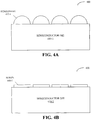
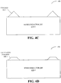
- FIGs. 4A-4D provide examples 400, 430, 450, and 470 that illustrate positive features fabricated on semiconductor dies 410, including: hemispheres 412, ridges, top-hat shapes or bumps 440, pyramids 460, and/or truncated pyramids 480. These features may mate with or couple to corresponding negative features facilitating 'snap-fit' assembly, thereby providing and maintaining precise alignment. Note that these negative features may include: slots, trenches, etch pits, pyramids, and/or truncated pyramids.
- Integrated hemispheres 412 provide a direct approach for achieving wafer-scale assembly of an MCM by supplementing or replacing the use of micro-spheres or balls (as illustrated in FIG. 1 ). These hemispheres may be defined on semiconductor die 410-1 using standard photoresist. Then, the photoresist may be annealed to reflow the material and to allow surface tension to draw the photoresist into hemispherical shapes. Next, the formed half lenses may be hard-baked into the solid-glass hemispheres 412, which are ready to be mated with etch pits (and more generally, negative features) on the opposing chip or semiconductor die in an MCM. Alternatively, metal bumps (such as bumps 440 in FIG. 4B ) may be lithographically patterned. These bumps may be reflowed and allowed to cool. During the cooling operation, surface tension may lead to the formation of hemispherical-shaped metal bumps.
- positive features may also be fabricated using a subtractive process, for example, by selective etching into a silicon substrate.
- a mask area may protect a portion of the substrate from etching. In this case, the region surrounding the mask area is etched.
- the etching may be self-limiting or self-terminating, such as anisotropic lithography along the ⁇ 111> crystallographic direction to produce pyramids 460 ( FIG. 4C ).
- etch stops are defined, for example, using CMOS technology.
- an isotropic etch may be used to produce a mesa or bump 440 ( FIG. 4B ) or to produce truncated pyramids 480 (in which the sides are along the ⁇ 111> crystallographic direction and top is, for example, along the ⁇ 100> crystallographic direction).
- truncated pyramids 480 may be fabricated by stopping an anisotropic etch prior to completion (such as when a desired etch depth is reached).
- examples 400 ( FIG. 4A ), 430 ( FIG. 4B ), 450 ( FIG. 4C ), and 470 (and the embodiments described below) are illustrated as having a limited number of positive features having a given configuration, other examples may include fewer components or additional components, two or more components may be combined into a single component, and/or a position of one or more components may be changed.
- the positive features may be fabricated in one or more directions.
- positive features such as hemispheres 412 ( FIG. 4A ) have a hexagonal-closed-packed configuration.
- a wide variety of materials may be used for the positive and/or negative features.
- a given semiconductor die includes both positive and negative features, thereby breaking the symmetry and ensuring that chips can only be assembled in one physical arrangement or orientation (note that another approach, described below with reference to FIG. 7 , uses a key-shaped feature).
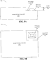
- FIGs. 5A and 5B provide block diagrams that illustrate a side-view 500 and a top-view 530 of an example of a semiconductor die 510.
- This example illustrates the combination of positive and negative features.
- negative feature 512 (defined by an etch depth 514) may be combined with positive feature 516.
- This configuration may be fabricated by etching negative feature 512 and then depositing positive feature 516.
- photoresist in the central area of positive feature 516 both features may be defined concurrently during an etch operation.
- the height of positive feature 516 may extend to the surface of semiconductor die 510, i.e., the height of positive feature 516 would equal the etch depth 514.
- This co-planar arrangement can promote alignment of semiconductor dies in an MCM , for example, by reducing misalignment 314 ( Fig. 3 ).
- an additional etch operation may be used to recess the top of the positive feature 516 relative to the surface of semiconductor die 510.
- FIGs. 6A and 6B provide block diagrams illustrating a side-view 600 and a top-view 630 of an example of a semiconductor die 610. This example also illustrates the combination of a positive feature 612 (defined by a height 614 relative to the surface of semiconductor die 610) and a negative feature 616. These features are configured to mate with those illustrated in FIGs. 5A and 5B to facilitate alignment of these semiconductor dies.
- a shape of a positive and/or a negative feature is used to determine an orientation of a semiconductor die or to limit the possible semiconductor dies that a given semiconductor die can mate with in an MCM (thereby facilitating self-assembly of an MCM ).
- FIG. 7 provides a block diagram of an embodiment 700 of a semiconductor die 710 that includes a key-shaped feature 712.
- either or both of the mating features on the semiconductor dies include a material, such as a soft metal to provide stress relief (for example, for stress due to relative motion or due to temperature differences) between coupled semiconductor dies.
- a material such as a soft metal to provide stress relief (for example, for stress due to relative motion or due to temperature differences) between coupled semiconductor dies.
- FIGs. 8A and 8B which provide block diagrams of embodiments 800 and 830 of semiconductor dies 810.
- positive feature 812 and/or corresponding negative feature 840 may include one or more layers, such as layers 814.
- micro-spheres may also allow micro-spheres in an MCM to couple power to one or more semiconductor dies.
- the micro-spheres are made of metal or have a metal (conductive) coating. These micro-spheres may or may not be used to align the semiconductor dies. For example, alignment is facilitated using positive and negative features and micro-spheres are used to couple power or other signals (such as optical signals) to the semiconductor dies.
- micro-spheres may include materials such as: sapphire, glass, silicon dioxide, and/or conductive materials (for example, a metal).
- micro-spheres are used in conjunction with positive and/or negative features to align semiconductor dies.
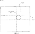
- FIG. 9 provides a block diagram illustrating a top-view of an embodiment of an MCM 900.
- This MCM includes semiconductor dies that have orthogonal trenches 910.
- a micro-sphere 912 maintains boundary conditions and constrains relative motion of the semiconductor dies in the Xand/or Ydirections.
- a soft metal layer, or a solid and/or liquid lubricant is included in one or more of the trenches 910 and/or on the micro-sphere 912.
- features, such as the trenches 910 may be defined to facilitate alignment but to also allow for motion associated with thermal expansion. For example, one trench may be 1 ⁇ m wide and the other may be 1.5 ⁇ m wide.
- FIG. 10 presents a flow chart illustrating an embodiment of a process 1000 for reducing misalignment between two semiconductor dies.
- a first semiconductor die is positioned relative to the second semiconductor die (1010).
- the first semiconductor die and the second semiconductor die are configured to communicate signals via proximity communication through a first set of proximity connectors proximate to a first surface of the first semiconductor die and a second set of proximity connectors proximate to a second surface of the second semiconductor die.
- a positive feature which is coupled to a third surface of the first semiconductor die, is coupled to a negative feature, which is coupled to a fourth surface of the second semiconductor die (1012).
- this coupling facilitates alignment of the first set of proximity connectors and the second set of proximity connectors.
- a first region around the positive feature defines a first plane and a second region around the negative feature defines a second plane, and the positive feature protrudes above the first plane and the negative feature is recessed below the second plane.
- process 1000 there may be additional or fewer operations, the order of the operations may be changed, and two or more operations may be combined into a single operation.
- FIG. 11 presents a block diagram illustrating a computer system 1100, which includes one or more processors 1110, a communication interface 1112, a user interface 1114, and one or more signal lines 1122 coupling these components together.
- the one or more processing units 1110 may support parallel processing and/or multi-threaded operation
- the communication interface 1112 may have a persistent communication connection
- the one or more signal lines 1122 may constitute a communication bus.
- the user interface 1114 may include: a display 1116, a keyboard 1118, and/or a pointer, such as a mouse 1120.
- Computer system 1100 may include memory 1124, which may include high speed random access memory and/or non-volatile memory. More specifically, memory 1124 may include: ROM, RAM, EPROM, EEPROM, FLASH, one or more smart cards, one or more magnetic disc storage devices, and/or one or more optical storage devices. Memory 1124 may store an operating system 1126, such as SOLARIS, LINUX, UNIX, OS X, or WINDOWS, that includes procedures (or a set of instructions) for handling various basic system services for performing hardware dependent tasks. Memory 1124 may also store procedures (or a set of instructions) in a communication module 1128. The communication procedures may be used for communicating with one or more computers and/or servers, including computers and/or servers that are remotely located with respect to the computer system 1100.
- memory 1124 may include high speed random access memory and/or non-volatile memory. More specifically, memory 1124 may include: ROM, RAM, EPROM, EEPROM, FLASH, one or more smart cards, one or more magnetic disc storage devices,
- Memory 1124 may also include the one or more program modules (of sets of instructions) 1130. Instructions in the program modules 1130 in the memory 1124 may be implemented in a high-level procedural language, an object-oriented programming language, and/or in an assembly or machine language. The programming language may be compiled or interpreted, i.e., configurable or configured to be executed by the one or more processing units 1110.
- Computer system 1100 may include one or more macro-chips 1108 (such as one or more MCMs) that include semiconductor dies that are aligned using positive and/or negative features as described.
- macro-chips 1108 such as one or more MCMs
- Computer system 1100 may include fewer components or additional components, two or more components may be combined into a single component, and/or a position of one or more components may be changed.
- the functionality of the computer system 1100 may be implemented more in hardware and less in software, or less in hardware and more in software, as is known in the art.
- FIG. 11 is intended to be a functional description of the various features that may be present in the computer system 1100 rather than as a structural schematic of the embodiments described herein.
- the functions of the computer system 1100 may be distributed over a large number of servers or computers, with various groups of the servers or computers performing particular subsets of the functions.
- some or all of the functionality of the computer system 1100 may be implemented in one or more application specific integrated circuits (ASICs) and/or one or more digital signal processors (DSPs).
- ASICs application specific integrated circuits
- DSPs digital signal processors
Landscapes
- Solid State Image Pick-Up Elements (AREA)
- Internal Circuitry In Semiconductor Integrated Circuit Devices (AREA)
Claims (4)
- Puce semi-conductrice (710), comprenant :des connecteurs de proximité (212) proches d'une première surface de la puce semi-conductrice, la puce semi-conductrice étant configurée pour communiquer par signaux avec une autre puce semi-conductrice par communication de proximité par le biais d'un ou plusieurs des connecteurs de proximité ; etun élément positif couplé à une deuxième surface de la puce semi-conductrice, une première région autour de l'élément positif définissant un premier plan et l'élément positif faisant saillie au-dessus du premier plan,caractérisé en ce que l'élément positif comporte une seule structure de clavette en forme de L (712) située à proximité d'un coin de la puce semi-conductrice qui spécifie une seule orientation en rotation dans le premier plan de la puce semi-conductrice par rapport à l'autre puce semi-conductrice pour aligner mécaniquement la puce semi-conductrice avec l'autre puce semi-conductrice, la puce semi-conductrice étant configurée pour s'accoupler avec une structure de clavette en forme de L négative correspondante de l'autre puce semi-conductrice à l'orientation en rotation.
- Puce semi-conductrice de la revendication 1, dans laquelle l'élément positif comporte une arête.
- Puce semi-conductrice de l'une quelconque des revendications précédentes, dans laquelle l'élément positif est un élément d'accouplement sur la puce semi-conductrice et comporte un matériau de relaxation des contraintes pour la relaxation des contraintes mécaniques quand la puce semi-conductrice est couplée à l'autre puce semi-conductrice.
- Système, comprenant :une première puce semi-conductrice formée par la puce semi-conductrice de l'une quelconque des revendications précédentes ; etune deuxième puce semi-conductrice formant l'autre puce semi-conductrice,dans lequel la deuxième puce semi-conductrice comporte un deuxième ensemble de connecteurs de proximité proches d'une première surface de la deuxième puce semi-conductrice et est configurée pour communiquer par signaux avec la première puce semi-conductrice par communication de proximité par le biais du deuxième ensemble de connecteurs de proximité ;dans lequel la deuxième puce semi-conductrice comporte un élément négatif couplé à une deuxième surface de la deuxième puce semi-conductrice ;dans lequel une région autour de l'élément négatif définit un premier plan de la deuxième puce semi-conductrice ;dans lequel l'élément négatif est en retrait sous le premier plan de la deuxième puce semi-conductrice ;dans lequel l'élément positif se couple à l'élément négatif à la seule orientation en rotation, facilitant ainsi l'alignement du premier ensemble de connecteurs de proximité et du deuxième ensemble de connecteurs de proximité ; etdans lequel l'élément négatif comporte une seule structure de clavette en forme de L correspondant à l'élément positif.
Applications Claiming Priority (2)
| Application Number | Priority Date | Filing Date | Title |
|---|---|---|---|
| US11/864,347 US7923845B2 (en) | 2007-09-28 | 2007-09-28 | Alignment features for proximity communication |
| PCT/US2008/076555 WO2009045711A1 (fr) | 2007-09-28 | 2008-09-16 | Caractéristiques d'alignement pour communication de proximité |
Publications (2)
| Publication Number | Publication Date |
|---|---|
| EP2201602A1 EP2201602A1 (fr) | 2010-06-30 |
| EP2201602B1 true EP2201602B1 (fr) | 2019-01-09 |
Family
ID=40110975
Family Applications (1)
| Application Number | Title | Priority Date | Filing Date |
|---|---|---|---|
| EP08799569.2A Active EP2201602B1 (fr) | 2007-09-28 | 2008-09-16 | Éléments d'alignement pour communication de proximité |
Country Status (4)
| Country | Link |
|---|---|
| US (1) | US7923845B2 (fr) |
| EP (1) | EP2201602B1 (fr) |
| TW (1) | TWI476871B (fr) |
| WO (1) | WO2009045711A1 (fr) |
Families Citing this family (11)
| Publication number | Priority date | Publication date | Assignee | Title |
|---|---|---|---|---|
| WO2006019911A1 (fr) * | 2004-07-26 | 2006-02-23 | Sun Microsystems, Inc. | Module multipuce et module monopuce pour puces et connecteurs de proximite |
| US8102020B2 (en) | 2006-05-18 | 2012-01-24 | Oracle America, Inc. | Equalization in proximity communication |
| US8212354B2 (en) * | 2009-12-17 | 2012-07-03 | Oracle America, Inc. | Active plastic bridge chips |
| US8564137B2 (en) | 2010-11-05 | 2013-10-22 | Stmicroelectronics, Inc. | System for relieving stress and improving heat management in a 3D chip stack having an array of inter-stack connections |
| US8653671B2 (en) * | 2010-11-05 | 2014-02-18 | Stmicroelectronics, Inc. | System for relieving stress and improving heat management in a 3D chip stack |
| US20140090234A1 (en) * | 2011-05-23 | 2014-04-03 | University Of Massachusetts | Apparatus and methods for multi-scale alignment and fastening |
| EP2769407B1 (fr) | 2011-10-21 | 2017-05-10 | Santa Barbara Infrared Inc. | Techniques de juxtaposition de matrices d'éléments de pixels |
| US9748214B2 (en) | 2011-10-21 | 2017-08-29 | Santa Barbara Infrared, Inc. | Techniques for tiling arrays of pixel elements and fabricating hybridized tiles |
| ITVI20120145A1 (it) | 2012-06-15 | 2013-12-16 | St Microelectronics Srl | Struttura comprensiva di involucro comprendente connessioni laterali |
| FR3062237B1 (fr) * | 2017-01-23 | 2020-05-01 | Commissariat A L'energie Atomique Et Aux Energies Alternatives | Procede de realisation d’une puce a circuit integre et puce a circuit integre. |
| US12598999B2 (en) * | 2022-05-23 | 2026-04-07 | International Business Machines Corporation | Multi-chip die alignment |
Family Cites Families (9)
| Publication number | Priority date | Publication date | Assignee | Title |
|---|---|---|---|---|
| US6495396B1 (en) | 2001-08-29 | 2002-12-17 | Sun Microsystems, Inc. | Method of coupling and aligning semiconductor devices including multi-chip semiconductor devices |
| US6885090B2 (en) | 2001-11-28 | 2005-04-26 | North Carolina State University | Inductively coupled electrical connectors |
| TWI280641B (en) * | 2001-12-28 | 2007-05-01 | Via Tech Inc | Chip structure |
| TWI245402B (en) * | 2002-01-07 | 2005-12-11 | Megic Corp | Rod soldering structure and manufacturing process thereof |
| US7018867B2 (en) | 2003-02-06 | 2006-03-28 | Intel Corporation | Fabricating stacked chips using fluidic templated-assembly |
| TW592013B (en) * | 2003-09-09 | 2004-06-11 | Advanced Semiconductor Eng | Solder bump structure and the method for forming the same |
| KR100555706B1 (ko) * | 2003-12-18 | 2006-03-03 | 삼성전자주식회사 | 미세 솔더볼 구현을 위한 ubm 및 이를 이용한 플립칩패키지 방법 |
| US7106079B2 (en) | 2004-10-22 | 2006-09-12 | Sun Microsystems, Inc. | Using an interposer to facilate capacitive communication between face-to-face chips |
| US7592707B2 (en) | 2005-10-03 | 2009-09-22 | Sun Microsystems, Inc. | Method and apparatus for facilitating proximity communication and power delivery |
-
2007
- 2007-09-28 US US11/864,347 patent/US7923845B2/en active Active
-
2008
- 2008-09-16 EP EP08799569.2A patent/EP2201602B1/fr active Active
- 2008-09-16 WO PCT/US2008/076555 patent/WO2009045711A1/fr not_active Ceased
- 2008-09-18 TW TW097135877A patent/TWI476871B/zh active
Non-Patent Citations (1)
| Title |
|---|
| None * |
Also Published As
| Publication number | Publication date |
|---|---|
| TW200931602A (en) | 2009-07-16 |
| TWI476871B (zh) | 2015-03-11 |
| WO2009045711A1 (fr) | 2009-04-09 |
| US7923845B2 (en) | 2011-04-12 |
| US20090085233A1 (en) | 2009-04-02 |
| EP2201602A1 (fr) | 2010-06-30 |
Similar Documents
| Publication | Publication Date | Title |
|---|---|---|
| EP2201602B1 (fr) | Éléments d'alignement pour communication de proximité | |
| EP2218103B1 (fr) | Module multipuce et communication de proximité entre des puces dans le module | |
| EP2815429B1 (fr) | Module à plusieurs puces comprenant une structure compressible et méthode de maintien d'alignement dans un module à plusieurs puces à l'aide d'une structure compressible | |
| EP2612356B1 (fr) | Boîtier de puces à empilement incliné à coudes statiques | |
| US8188581B2 (en) | Mechanical coupling in a multi-chip module using magnetic components | |
| EP2609623B1 (fr) | Communication optique dans un boîtier de puces à empilement en rampe | |
| EP2612355B1 (fr) | Boîtier de puces empilées avec rampe et son procédé de fabrication | |
| US7888175B2 (en) | Method and apparatus for facilitating proximity communication and power delivery | |
| US11735528B2 (en) | Semiconductor memory stacks connected to processing units and associated systems and methods | |
| EP1443559B1 (fr) | Module d'ensemble de circuits intégrés | |
| US8975754B2 (en) | Chip package for high-count chip stacks | |
| US20110278718A1 (en) | Assembly of multi-chip modules using reflowable features | |
| CN116314090A (zh) | 包括采用不同焊料材料的互连的微电子组件 | |
| US8531042B2 (en) | Technique for fabricating microsprings on non-planar surfaces | |
| US20110149539A1 (en) | Base plate for use in a multi-chip module | |
| WO2009045712A1 (fr) | Auto-assemblage de micro-structures | |
| US7514289B2 (en) | Methods and structures for facilitating proximity communication | |
| EP4020032B1 (fr) | Architectures de rainure de silicium et procédés de fabrication d'alignement passif dans une puce photonique | |
| US8487429B2 (en) | Assembly of multi-chip modules using sacrificial features | |
| CN121712084A (zh) | 半导体结构及其制备方法和半导体器件 | |
| WO2026066395A1 (fr) | Structure d'encapsulation de puce, son procédé de fabrication et dispositif électronique |
Legal Events
| Date | Code | Title | Description |
|---|---|---|---|
| PUAI | Public reference made under article 153(3) epc to a published international application that has entered the european phase |
Free format text: ORIGINAL CODE: 0009012 |
|
| 17P | Request for examination filed |
Effective date: 20100409 |
|
| AK | Designated contracting states |
Kind code of ref document: A1 Designated state(s): AT BE BG CH CY CZ DE DK EE ES FI FR GB GR HR HU IE IS IT LI LT LU LV MC MT NL NO PL PT RO SE SI SK TR |
|
| AX | Request for extension of the european patent |
Extension state: AL BA MK RS |
|
| RAP1 | Party data changed (applicant data changed or rights of an application transferred) |
Owner name: ORACLE AMERICA, INC. |
|
| RIN1 | Information on inventor provided before grant (corrected) |
Inventor name: KRISHNAMOORTHY, ASHOK V. Inventor name: MITCHELL, JAMES G. Inventor name: CUNNINGHAM, JOHN E. |
|
| DAX | Request for extension of the european patent (deleted) | ||
| STAA | Information on the status of an ep patent application or granted ep patent |
Free format text: STATUS: EXAMINATION IS IN PROGRESS |
|
| 17Q | First examination report despatched |
Effective date: 20161216 |
|
| GRAP | Despatch of communication of intention to grant a patent |
Free format text: ORIGINAL CODE: EPIDOSNIGR1 |
|
| STAA | Information on the status of an ep patent application or granted ep patent |
Free format text: STATUS: GRANT OF PATENT IS INTENDED |
|
| RIC1 | Information provided on ipc code assigned before grant |
Ipc: H01L 23/48 20060101ALI20180704BHEP Ipc: H01L 29/06 20060101ALI20180704BHEP Ipc: H01L 21/98 20060101AFI20180704BHEP Ipc: H01L 25/065 20060101ALI20180704BHEP Ipc: H01L 23/544 20060101ALI20180704BHEP |
|
| INTG | Intention to grant announced |
Effective date: 20180727 |
|
| GRAS | Grant fee paid |
Free format text: ORIGINAL CODE: EPIDOSNIGR3 |
|
| GRAA | (expected) grant |
Free format text: ORIGINAL CODE: 0009210 |
|
| STAA | Information on the status of an ep patent application or granted ep patent |
Free format text: STATUS: THE PATENT HAS BEEN GRANTED |
|
| AK | Designated contracting states |
Kind code of ref document: B1 Designated state(s): AT BE BG CH CY CZ DE DK EE ES FI FR GB GR HR HU IE IS IT LI LT LU LV MC MT NL NO PL PT RO SE SI SK TR |
|
| REG | Reference to a national code |
Ref country code: GB Ref legal event code: FG4D |
|
| REG | Reference to a national code |
Ref country code: CH Ref legal event code: EP Ref country code: AT Ref legal event code: REF Ref document number: 1088379 Country of ref document: AT Kind code of ref document: T Effective date: 20190115 |
|
| REG | Reference to a national code |
Ref country code: DE Ref legal event code: R096 Ref document number: 602008058704 Country of ref document: DE |
|
| REG | Reference to a national code |
Ref country code: IE Ref legal event code: FG4D |
|
| REG | Reference to a national code |
Ref country code: NL Ref legal event code: MP Effective date: 20190109 |
|
| REG | Reference to a national code |
Ref country code: LT Ref legal event code: MG4D |
|
| PG25 | Lapsed in a contracting state [announced via postgrant information from national office to epo] |
Ref country code: NL Free format text: LAPSE BECAUSE OF FAILURE TO SUBMIT A TRANSLATION OF THE DESCRIPTION OR TO PAY THE FEE WITHIN THE PRESCRIBED TIME-LIMIT Effective date: 20190109 |
|
| REG | Reference to a national code |
Ref country code: AT Ref legal event code: MK05 Ref document number: 1088379 Country of ref document: AT Kind code of ref document: T Effective date: 20190109 |
|
| PG25 | Lapsed in a contracting state [announced via postgrant information from national office to epo] |
Ref country code: ES Free format text: LAPSE BECAUSE OF FAILURE TO SUBMIT A TRANSLATION OF THE DESCRIPTION OR TO PAY THE FEE WITHIN THE PRESCRIBED TIME-LIMIT Effective date: 20190109 Ref country code: SE Free format text: LAPSE BECAUSE OF FAILURE TO SUBMIT A TRANSLATION OF THE DESCRIPTION OR TO PAY THE FEE WITHIN THE PRESCRIBED TIME-LIMIT Effective date: 20190109 Ref country code: FI Free format text: LAPSE BECAUSE OF FAILURE TO SUBMIT A TRANSLATION OF THE DESCRIPTION OR TO PAY THE FEE WITHIN THE PRESCRIBED TIME-LIMIT Effective date: 20190109 Ref country code: PT Free format text: LAPSE BECAUSE OF FAILURE TO SUBMIT A TRANSLATION OF THE DESCRIPTION OR TO PAY THE FEE WITHIN THE PRESCRIBED TIME-LIMIT Effective date: 20190509 Ref country code: NO Free format text: LAPSE BECAUSE OF FAILURE TO SUBMIT A TRANSLATION OF THE DESCRIPTION OR TO PAY THE FEE WITHIN THE PRESCRIBED TIME-LIMIT Effective date: 20190409 Ref country code: LT Free format text: LAPSE BECAUSE OF FAILURE TO SUBMIT A TRANSLATION OF THE DESCRIPTION OR TO PAY THE FEE WITHIN THE PRESCRIBED TIME-LIMIT Effective date: 20190109 Ref country code: PL Free format text: LAPSE BECAUSE OF FAILURE TO SUBMIT A TRANSLATION OF THE DESCRIPTION OR TO PAY THE FEE WITHIN THE PRESCRIBED TIME-LIMIT Effective date: 20190109 |
|
| PG25 | Lapsed in a contracting state [announced via postgrant information from national office to epo] |
Ref country code: BG Free format text: LAPSE BECAUSE OF FAILURE TO SUBMIT A TRANSLATION OF THE DESCRIPTION OR TO PAY THE FEE WITHIN THE PRESCRIBED TIME-LIMIT Effective date: 20190409 Ref country code: HR Free format text: LAPSE BECAUSE OF FAILURE TO SUBMIT A TRANSLATION OF THE DESCRIPTION OR TO PAY THE FEE WITHIN THE PRESCRIBED TIME-LIMIT Effective date: 20190109 Ref country code: GR Free format text: LAPSE BECAUSE OF FAILURE TO SUBMIT A TRANSLATION OF THE DESCRIPTION OR TO PAY THE FEE WITHIN THE PRESCRIBED TIME-LIMIT Effective date: 20190410 Ref country code: IS Free format text: LAPSE BECAUSE OF FAILURE TO SUBMIT A TRANSLATION OF THE DESCRIPTION OR TO PAY THE FEE WITHIN THE PRESCRIBED TIME-LIMIT Effective date: 20190509 Ref country code: LV Free format text: LAPSE BECAUSE OF FAILURE TO SUBMIT A TRANSLATION OF THE DESCRIPTION OR TO PAY THE FEE WITHIN THE PRESCRIBED TIME-LIMIT Effective date: 20190109 |
|
| REG | Reference to a national code |
Ref country code: DE Ref legal event code: R097 Ref document number: 602008058704 Country of ref document: DE |
|
| PG25 | Lapsed in a contracting state [announced via postgrant information from national office to epo] |
Ref country code: SK Free format text: LAPSE BECAUSE OF FAILURE TO SUBMIT A TRANSLATION OF THE DESCRIPTION OR TO PAY THE FEE WITHIN THE PRESCRIBED TIME-LIMIT Effective date: 20190109 Ref country code: CZ Free format text: LAPSE BECAUSE OF FAILURE TO SUBMIT A TRANSLATION OF THE DESCRIPTION OR TO PAY THE FEE WITHIN THE PRESCRIBED TIME-LIMIT Effective date: 20190109 Ref country code: RO Free format text: LAPSE BECAUSE OF FAILURE TO SUBMIT A TRANSLATION OF THE DESCRIPTION OR TO PAY THE FEE WITHIN THE PRESCRIBED TIME-LIMIT Effective date: 20190109 Ref country code: EE Free format text: LAPSE BECAUSE OF FAILURE TO SUBMIT A TRANSLATION OF THE DESCRIPTION OR TO PAY THE FEE WITHIN THE PRESCRIBED TIME-LIMIT Effective date: 20190109 Ref country code: DK Free format text: LAPSE BECAUSE OF FAILURE TO SUBMIT A TRANSLATION OF THE DESCRIPTION OR TO PAY THE FEE WITHIN THE PRESCRIBED TIME-LIMIT Effective date: 20190109 Ref country code: AT Free format text: LAPSE BECAUSE OF FAILURE TO SUBMIT A TRANSLATION OF THE DESCRIPTION OR TO PAY THE FEE WITHIN THE PRESCRIBED TIME-LIMIT Effective date: 20190109 Ref country code: IT Free format text: LAPSE BECAUSE OF FAILURE TO SUBMIT A TRANSLATION OF THE DESCRIPTION OR TO PAY THE FEE WITHIN THE PRESCRIBED TIME-LIMIT Effective date: 20190109 |
|
| PLBE | No opposition filed within time limit |
Free format text: ORIGINAL CODE: 0009261 |
|
| STAA | Information on the status of an ep patent application or granted ep patent |
Free format text: STATUS: NO OPPOSITION FILED WITHIN TIME LIMIT |
|
| 26N | No opposition filed |
Effective date: 20191010 |
|
| PG25 | Lapsed in a contracting state [announced via postgrant information from national office to epo] |
Ref country code: SI Free format text: LAPSE BECAUSE OF FAILURE TO SUBMIT A TRANSLATION OF THE DESCRIPTION OR TO PAY THE FEE WITHIN THE PRESCRIBED TIME-LIMIT Effective date: 20190109 |
|
| PG25 | Lapsed in a contracting state [announced via postgrant information from national office to epo] |
Ref country code: TR Free format text: LAPSE BECAUSE OF FAILURE TO SUBMIT A TRANSLATION OF THE DESCRIPTION OR TO PAY THE FEE WITHIN THE PRESCRIBED TIME-LIMIT Effective date: 20190109 |
|
| PG25 | Lapsed in a contracting state [announced via postgrant information from national office to epo] |
Ref country code: MC Free format text: LAPSE BECAUSE OF FAILURE TO SUBMIT A TRANSLATION OF THE DESCRIPTION OR TO PAY THE FEE WITHIN THE PRESCRIBED TIME-LIMIT Effective date: 20190109 |
|
| REG | Reference to a national code |
Ref country code: CH Ref legal event code: PL |
|
| PG25 | Lapsed in a contracting state [announced via postgrant information from national office to epo] |
Ref country code: IE Free format text: LAPSE BECAUSE OF NON-PAYMENT OF DUE FEES Effective date: 20190916 Ref country code: LU Free format text: LAPSE BECAUSE OF NON-PAYMENT OF DUE FEES Effective date: 20190916 Ref country code: LI Free format text: LAPSE BECAUSE OF NON-PAYMENT OF DUE FEES Effective date: 20190930 Ref country code: CH Free format text: LAPSE BECAUSE OF NON-PAYMENT OF DUE FEES Effective date: 20190930 |
|
| REG | Reference to a national code |
Ref country code: BE Ref legal event code: MM Effective date: 20190930 |
|
| PG25 | Lapsed in a contracting state [announced via postgrant information from national office to epo] |
Ref country code: BE Free format text: LAPSE BECAUSE OF NON-PAYMENT OF DUE FEES Effective date: 20190930 |
|
| PG25 | Lapsed in a contracting state [announced via postgrant information from national office to epo] |
Ref country code: FR Free format text: LAPSE BECAUSE OF NON-PAYMENT OF DUE FEES Effective date: 20190930 |
|
| PG25 | Lapsed in a contracting state [announced via postgrant information from national office to epo] |
Ref country code: CY Free format text: LAPSE BECAUSE OF FAILURE TO SUBMIT A TRANSLATION OF THE DESCRIPTION OR TO PAY THE FEE WITHIN THE PRESCRIBED TIME-LIMIT Effective date: 20190109 |
|
| PG25 | Lapsed in a contracting state [announced via postgrant information from national office to epo] |
Ref country code: HU Free format text: LAPSE BECAUSE OF FAILURE TO SUBMIT A TRANSLATION OF THE DESCRIPTION OR TO PAY THE FEE WITHIN THE PRESCRIBED TIME-LIMIT; INVALID AB INITIO Effective date: 20080916 Ref country code: MT Free format text: LAPSE BECAUSE OF FAILURE TO SUBMIT A TRANSLATION OF THE DESCRIPTION OR TO PAY THE FEE WITHIN THE PRESCRIBED TIME-LIMIT Effective date: 20190109 |
|
| P01 | Opt-out of the competence of the unified patent court (upc) registered |
Effective date: 20230522 |
|
| PGFP | Annual fee paid to national office [announced via postgrant information from national office to epo] |
Ref country code: DE Payment date: 20250730 Year of fee payment: 18 |
|
| PGFP | Annual fee paid to national office [announced via postgrant information from national office to epo] |
Ref country code: GB Payment date: 20250731 Year of fee payment: 18 |
|
| REG | Reference to a national code |
Ref country code: DE Ref legal event code: R079 Ref document number: 602008058704 Country of ref document: DE Free format text: PREVIOUS MAIN CLASS: H01L0021980000 Ipc: H10W0090240000 |