EP2201619B1 - Composant piézo-électrique multicouche - Google Patents
Composant piézo-électrique multicouche Download PDFInfo
- Publication number
- EP2201619B1 EP2201619B1 EP08835093.9A EP08835093A EP2201619B1 EP 2201619 B1 EP2201619 B1 EP 2201619B1 EP 08835093 A EP08835093 A EP 08835093A EP 2201619 B1 EP2201619 B1 EP 2201619B1
- Authority
- EP
- European Patent Office
- Prior art keywords
- layer
- piezoceramic
- layers
- multilayer component
- structured
- Prior art date
- Legal status (The legal status is an assumption and is not a legal conclusion. Google has not performed a legal analysis and makes no representation as to the accuracy of the status listed.)
- Not-in-force
Links
Images

Classifications
-
- H—ELECTRICITY
- H10—SEMICONDUCTOR DEVICES; ELECTRIC SOLID-STATE DEVICES NOT OTHERWISE PROVIDED FOR
- H10N—ELECTRIC SOLID-STATE DEVICES NOT OTHERWISE PROVIDED FOR
- H10N30/00—Piezoelectric or electrostrictive devices
- H10N30/01—Manufacture or treatment
- H10N30/05—Manufacture of multilayered piezoelectric or electrostrictive devices, or parts thereof, e.g. by stacking piezoelectric bodies and electrodes
- H10N30/053—Manufacture of multilayered piezoelectric or electrostrictive devices, or parts thereof, e.g. by stacking piezoelectric bodies and electrodes by integrally sintering piezoelectric or electrostrictive bodies and electrodes
-
- H—ELECTRICITY
- H10—SEMICONDUCTOR DEVICES; ELECTRIC SOLID-STATE DEVICES NOT OTHERWISE PROVIDED FOR
- H10N—ELECTRIC SOLID-STATE DEVICES NOT OTHERWISE PROVIDED FOR
- H10N30/00—Piezoelectric or electrostrictive devices
- H10N30/50—Piezoelectric or electrostrictive devices having a stacked or multilayer structure
- H10N30/508—Piezoelectric or electrostrictive devices having a stacked or multilayer structure adapted for alleviating internal stress, e.g. cracking control layers
-
- Y—GENERAL TAGGING OF NEW TECHNOLOGICAL DEVELOPMENTS; GENERAL TAGGING OF CROSS-SECTIONAL TECHNOLOGIES SPANNING OVER SEVERAL SECTIONS OF THE IPC; TECHNICAL SUBJECTS COVERED BY FORMER USPC CROSS-REFERENCE ART COLLECTIONS [XRACs] AND DIGESTS
- Y10—TECHNICAL SUBJECTS COVERED BY FORMER USPC
- Y10T—TECHNICAL SUBJECTS COVERED BY FORMER US CLASSIFICATION
- Y10T29/00—Metal working
- Y10T29/42—Piezoelectric device making
Definitions
- a piezoelectric multilayer component in particular a piezoelectric multilayer component with intentionally partially delaminatable piezoceramic layers, is described.
- electrode layers are deposited only on a portion of a piezoceramic layer.
- the remaining area on the piezoceramic layer is thus electrically insulating in order to avoid short circuits between an external contact and a counter-pole electrode layer.
- This region free of an electrode layer may be referred to as an inactive zone.
- WO 2006/087871-A1 is a piezoelectric multilayer component with side-mounted, crack-inducing, electrically conductive layers known.
- An object to be solved is to specify a piezoelectric multilayer component which has an improved deflection path.
- a further object to be achieved is to specify a piezoelectric multilayer component which has an improved deflection path and remains functional over a relatively long period of time.
- a piezoelectric multilayer component with a stack of piezoceramic layers and electrode layers arranged one above another is specified, wherein at least one piezoceramic layer having a layer patterned according to a predetermined pattern is printed in a piezoelectrically inactive zone.
- the structured layer has at least one connecting element, by means of which adjacent piezoceramic layers having a first strength are mechanically connected to one another in the stacking direction.
- the structured layer has, in addition to the connecting elements, gaps that are filled with piezoceramic material of the adjacent piezoceramic layers.
- the gap may be completely or only partially, ie filled with remaining gaps, with the piezoceramic material.
- the mechanical connection between the adjacent piezoceramic layers in the intermediate space or in the region of the intermediate space next to the connecting elements has a second strength, which is lower than that above called first strength.
- the second strength of the mechanical connection between the adjacent piezoceramic layers is less than the strength of the mechanical connection between the adjacent piezoceramic layers in the active zone of the multilayer component.
- the structured layer can also be designed as a continuous, i. gapless or at least almost complete layer can be considered.
- the structured layer has regions which are mechanically more firmly bonded to the adjacent piezoceramic layer than other regions of the structured layer.
- the connecting elements of the structured layers furthermore ensure that two piezoceramic layers adjacent to one another in the stacking direction make mechanical contact with one another at their respective edge regions, in particular so that the multilayer component is not broken or destroyed during its production, before the stack is pressed.
- the structured layer is located at least in the inactive zone of the multilayer component, which is exposed to the described clamping effect. However, it can extend into the active zone further inside the multilayer component. Connecting elements and the spaces next to them can thus extend into the active zone of the multilayer component.
- the piezoceramic layers Due to the regions in which the adjacent piezoceramic layers are bonded together in the inactive zone with reduced strength, the piezoceramic layers can partially delaminate upon application of an operating voltage to the multilayer component. They are pulled along by the expansion of the multilayer component in the middle region or in its active zone with reduced resistance. As a result, a clamping effect between the active and the inactive zone of the multilayer component can be avoided or at least reduced. Thus, the entire deflection path of the piezoelectric multilayer component, in particular in the axially central region of the stack, can be increased.
- the partial delamination of the piezoceramic layers in the inactive zone due to the lower mechanical connection there has the advantageous effect that the multilayer component is mechanically relieved of tensile or clamping stresses there, so there is no uncontrolled cracking within the stack, in particular between two opposite pole electrode layers, can come.
- the duration of the functionality of the piezoelectric multilayer component can be extended.
- the structured layer comprises cylindrical connecting elements, which could have a circular or a polygonal outline.
- the at least one connecting element is lattice-shaped, wherein a plurality of lines of material printed on the piezoceramic layer intersect and thereby include interspaces which are filled with material of adjacent piezoceramic layers.
- a connecting element of a structured layer may be annular.
- a plurality of annular connecting elements of a structured layer are arranged concentrically on a piezoceramic layer next to one another and connect adjacent piezoceramic layers in the stack.
- the annular connecting elements are filled with the material of adjacent piezoceramic layers gaps.
- the connecting elements or the areas filled with piezoceramic material next to them can be shaped as desired.
- the structured layer has a plurality of uniformly distributed on the piezoceramic layer connecting elements. These can be arranged substantially homogeneously or equidistant from each other.
- the electrode layers of the stack preferably contain one of the following materials or alloys: silver, palladium, nickel, copper.
- the piezoceramic layers preferably contain a ceramic based on lead zirconate titanate (PZT).
- PZT lead zirconate titanate
- the structured layer or a connecting element of the layer contains a material which is contained in a piezoceramic layer connected to it. In this case, undesired chemical reactions, in particular during the production of the multilayer component, are advantageously between the structured Layer and a connected with her piezoceramic layer avoided. Additionally or alternatively, the structured layer or an at least one connecting element encompassed by it may contain a metal, which is also contained in an electrode layer.
- the structured layer is arranged on the same piezoceramic layer as an electrode layer. However, it may also be arranged on another piezoceramic layer than on one on which an electrode layer is arranged. This results in the advantage that with a suitable mask comprising different patterns, in each case for an electrode layer and for a structured layer, at the same time an electrode layer and a structured layer of the type described can be applied to a piezoceramic layer.
- a plurality of structured layers are distributed on a plurality of piezoceramic layers over the height of the stack of the multilayer component.
- a cumulative reduced clamping effect thereby advantageously further increases the achievable deflection path of the piezoelectric multilayer component.
- the electrode layers of the multilayer component are preferably contacted with an external contact designed as a layer, which is arranged on an outer surface of the stack running parallel to the stacking direction.
- an external contact designed as a layer, which is arranged on an outer surface of the stack running parallel to the stacking direction.
- other forms of external contact are possible, such as cable or rod-shaped.
- the piezoceramic layer printed with a structured layer may be a piezoceramic layer already printed with an electrode layer.
- the structured layer preferably at a distance from the electrode layer, is applied to the piezoceramic layer next to it.
- piezoceramic layers printed with electrode layers a plurality of unprinted piezoceramic layers can be stacked on top of one another. These can each be printed with structured layers of the type described.
- the invention relates to a method for producing a piezoelectric multilayer component, in which a stack of electrode layers and printed piezoceramic layers is formed. These are piezoceramic green films and electrode material printed on each layer as such.
- the piezoceramic films can already be pretreated by temperature during stacking and / or already contain additives which promote their handling during production or transport. These may be organic binders.
- At least one piezoceramic layer is printed before stacking at least in a piezoelectrically inactive zone in the respective edge region of the piezoceramic layer with a layer structured with a predetermined pattern.
- the predetermined pattern of the structured layer printed on the at least one piezoceramic layer results in connecting elements and existing between them Interspaces, which are initially cavities or gaps.
- the connecting elements connect adjacent piezoceramic layers with each other during and after stacking.
- the printing of the at least one piezoceramic layer is preferably carried out by means of a screen printing process.
- the compression of a material through the holes or recesses of the screen yields the pattern, in particular the connecting elements of the pattern.
- the material may be a piezoceramic material or an electrically conductive material, in particular also a material which is used for the electrode layers.
- the stack can then be pressed, so that piezoceramic layers soften slightly and their respective material flows into the gaps or interstices of a structured layer arranged between them.
- the piezoceramic layers liquefy sufficiently under pressure and elevated temperature in order to fill the gaps of the structured layer at least sufficiently so that they mechanically bond in the intermediate space next to the connecting elements.
- this results in a mechanical connection between the adjacent piezoceramic layer in said interstices, which is less solid than the mechanical connection between the piezoelectric layers resulting from the connecting elements during compression.
- the reason for the lower second strength of the mechanical connection between the adjacent piezoelectric layers in the interstices is that there the connection does not prevail over a pressing force is achieved, but only on the taking place in the spaces available for this purpose mixing and bonding of the materials of the piezoceramic layers.
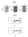
- Figure 1A shows a longitudinal section of a piezoelectric multilayer component with a stack 1 of stacked piezoceramic layers 2 and electrode layers 3, which exclusively with a Dielectric filled space between two identically poled electrode layers forms an inactive zone IZ and the overlapping in orthogonal projection region between opposing electrode layers is an active zone AZ of the multilayer component, which expands at applied operating voltage in the longitudinal direction.
- layers external contacts 5a and 5b are shown, which are arranged on the perpendicular to the piezoceramic layers 2 extending side surfaces of the multilayer component. Between two adjacent electrode layers 3, several piezoceramic layers 2 may be present.
- the external contacts 5a, 5b may be baked by means of a metal paste or applied galvanically to the side surface (s) of the stack.
- FIG. 1B is a side cross-sectional view of a portion of a stack 1, wherein between two adjacent in the stacking direction electrode layers 3 more piezoceramic layers 2 are arranged or stacked one above the other.
- the broken lines of the figure show the boundaries between two adjacent piezoceramic layers.
- FIGS. 2A to 2E each show areas of a multilayer component with a structure according to Figure 1A respectively.
- FIG. 1B
- FIG. 2A shows the positions of structured layers 4 on the basis of fat-drawn horizontal lines, with which piezoceramic layers 2 adjacent in the stacking direction are joined together mechanically less firmly than they are connected to each other further inside the stack.
- FIG. 2B shows a sectional view of the piezoelectric multilayer component according to FIG. 2A , wherein a single structured layer 4 is provided on each of a piezoceramic layer 2 between two adjacent electrode layers 3 in the stacking direction.
- the one with the Figure 2C pictured portion of the stack of a multilayer component corresponds to that of FIG. 2A , but with the difference that the areal expansions of the structured layers 4 parallel to the piezoceramic layer are smaller than those according to FIG. 2A ,
- the structured layers 4 are only in inactive zones IZ (see Figure 1A ) of the stack 1, in which nominally no or only a minimal extension of the stack in the longitudinal direction caused by a piezoelectric effect comes about.
- FIG. 2D is a sectional view of the piezoelectric multilayer component according to FIG. 2A respectively.
- Figure 2C wherein in each case on a piezoceramic layer 2, which is arranged between two adjacent in the stacking direction electrode layers 3, two structured layers 4 are arranged.
- the area expansions parallel to the piezoceramic layer of the structured layers 4 are greater than according to the figures of FIGS FIGS. 2A and 2C shown, wherein the structured layers of active zones AZ between adjacent, opposing electrode layers 3 to a side surface on which an external contact 5a and 5b according to Figure 1A can be arranged rich.
- Figure 2E shows a sectional view of a piezoelectric multilayer component, wherein in each case a structured layer 4 is arranged on the same piezoceramic layer 2, as an electrode layer 3.
- the respective structured layers 4 are arranged only in inactive zones IZ of the stack 1 of the multilayer component.
- FIG. 3A is a plan view of a structured layer 4, the cylindrical, preferably circular outlines having connecting elements 4a.
- the pattern of the printed on the piezoceramic layer, structured layer is thus one of spaced apart, pillar-shaped connecting elements.
- the connecting elements 4a can be applied to the corresponding piezoceramic layer in this pattern by means of, for example, a screen printing method, wherein the positioning of the connecting elements within the stack according to the preceding FIGS. 2A to 2E could be organized.
- the structured layers can be arranged next to an electrode layer 3 or next to an unprinted area of a piezoceramic layer 2, for which reason the area next to the structured layer 4 in this figure is marked with both reference symbols 2 and 3.
- the connecting elements 4a are continuous and two in the stacking direction connected adjacent piezoceramic layers 2. They are already in the state of the pile before being pressed.
- the structured layer comprises, in addition to the connecting elements 4 a, at least one or more gaps or cavities 4 b, at least prior to the pressing of the stack.
- FIG. 3B shows a lattice-shaped connecting element 4a of a structured layer 4, which is arranged on an edge region of a piezoceramic layer 3 and can extend to an arranged on a side surface of the stack external contact.
- This connection structure can also be printed on the piezoceramic layer by means of a screen printing process.
- FIG. 3C shows an alternative embodiment of a structured layer 4, whose structures or connecting elements 4a are arranged annularly and concentrically in an edge region of a piezoceramic layer 3.
- the respective connecting elements are rectangular.
- the connecting elements 4a of the structured layer 4 can be printed on the desired piezoceramic layer 2 by the correspondingly shaped recesses of a mask.
- a ceramic or metallic material may be pressed through a screen or mask to produce the desired pattern on the piezoceramic layer.
- FIG. 4a shows a longitudinal section of a portion of the stack already shown with the previous figures, wherein the area shown comprises a piezoelectrically inactive zone of the stack.
- Stacked adjacent piezoceramic layers 2 are shown, between which a structured layer 4 is arranged.
- This comprises a plurality of connecting elements 4a in the form of upright cylinders or pillars, by means of which the corresponding piezoceramic layers are already connected to one another.
- spaces 4b are present.
- the intermediate spaces are first filled with air or with a medium which can be removed during pressing before being pressed.
- FIG. 4b shows the state of the with the FIG. 4b shown portion of the stack during or after the pressing of the stack.
- the previously existing gaps 4b are now filled due to the pressing process with material of the piezoceramic layers 2, in such a way that a mechanical connection between the piezoceramic layers comes about by the or the spaces next to the connecting elements 4a.
- the strength of the mechanical connection in the region of the connecting elements produced during pressing is still higher than that in the region of the spaces filled with the piezoceramic material.
- the areas of the piezoceramic layers on which the patterned layers 4 are deposited may be larger, smaller, or the same size as the area of an insulating region between an electrode layer and an external contact of opposite polarity disposed on a side surface of the stack.
- the structure, structures or connecting elements of a structured layer can consist of a metal or of an electrically non-conductive material or at least contain the corresponding materials.
- these materials are identical to those in the electrode layers or in the piezoceramic layers of the same piezoelectric multilayer component.
- this makes it possible to prevent additional chemical reactions between different materials of the multilayer component, in particular during its production.
- the number of piezoceramic layers, to which the described structured layers are applied can be of any desired size.
- a structured layer of the type described is applied to at least one piezoceramic layer.
- the following table shows preferred relationships between the sum of the areas of the interconnecting elements 4a of a patterned layer and the sum of the areas of the spaces 4b adjacent to the interconnecting elements.
- Sum of surfaces of fasteners Sum of areas of spaces prefers from 10 to 1 to 1 to 10 Further preferred from 2 to 1 from 1 to 4 LIST OF REFERENCE NUMBERS 1 Stack with piezoceramic layers and electrode layers 2 piezoceramic layer 3 electrode layer 4 structured layer 4a Connecting element of a structured layer 4b Interspace next to a connecting element 5a first external contact 5b second external contact IZ Inactive zone of the pile AZ Active zone of the pile
Landscapes
- Engineering & Computer Science (AREA)
- Manufacturing & Machinery (AREA)
- General Electrical Machinery Utilizing Piezoelectricity, Electrostriction Or Magnetostriction (AREA)
- Fuel-Injection Apparatus (AREA)
Claims (15)
- Composant piézoélectrique multicouche présentant un empilement (1) de couches céramiques (2) et de couches d'électrodes (3) disposées les unes au-dessus des autres, et dans lequel
au moins une couche piézocéramique est imprimée par une couche (4) structurée selon un motif prédéterminé dans une zone piézoélectriquement inactive (IZ) de l'empilement,
la couche structurée présente au moins un élément de liaison (4a) par lequel des couches piézocéramiques voisines dans la direction de l'empilement sont reliées mécaniquement les unes aux autres à une première résistance mécanique,
la couche structurée présente des espaces intermédiaires (4b) remplis au moins en partie de matériau piézocéramique des couches piézocéramiques voisines et
dans les espaces intermédiaires, les couches piézocéramiques voisines sont reliées mécaniquement les unes aux autres à une deuxième résistance mécanique plus basse que la première résistance mécanique. - Composant piézoélectrique multicouche selon la revendication 1, dans lequel la liaison mécanique à une deuxième résistance mécanique entre des couches piézocéramiques voisines (2) se forme dans les espaces intermédiaires (4b) pendant une compression de l'empilement du composant multicouche.
- Composant piézoélectrique multicouche selon l'une des revendications précédentes, dans lequel les éléments de liaison (4a) comportent des structures cylindriques debout.
- Composant piézoélectrique multicouche selon la revendication 3, dans lequel les structures cylindriques sont agencées à distance mutuelle de manière régulière.
- Composant piézoélectrique multicouche selon l'une des revendications précédentes, dans lequel le ou les éléments de liaison (4a) comportent une structure (4b) en forme de grille.
- Composant piézoélectrique multicouche selon l'une des revendications précédentes, dans lequel le ou les éléments de liaison (4a) comportent une structure (4b) en forme d'anneau.
- Composant piézoélectrique multicouche selon la revendication 6, dans lequel la couche structurée (4) comporte plusieurs éléments de liaison (4a) qui présentent la forme de plusieurs structures annulaires disposées concentriquement.
- Composant piézoélectrique multicouche selon l'une des revendications précédentes, dans lequel la couche structurée (4) contient le même métal que celui que contiennent les couches d'électrodes (3).
- Composant piézoélectrique multicouche selon l'une des revendications précédentes, dans lequel la couche structurée (4) contient le même métal que celui que contiennent les couches piézocéramiques (2).
- Composant piézoélectrique multicouche selon l'une des revendications précédentes, dans lequel la couche structurée (4) est disposée sur la même couche piézocéramique (2) que la couche d'électrode (3).
- Composant piézoélectrique multicouche selon l'une des revendications 1 à 9, dans lequel la couche structurée (4) est disposée sur une autre couche piézocéramique (2) que celle sur laquelle une couche d'électrode (3) est disposée.
- Composant piézoélectrique multicouche selon l'une des revendications précédentes, dans lequel la couche structurée (4) est de plus imprimée dans la zone active (AZ) de l'empilement (1) sur une couche piézoélectrique (2).
- Composant piézoélectrique multicouche selon l'une des revendications précédentes, dans lequel plusieurs couches structurées (4) sont réparties sur plusieurs couches piézocéramiques (2) suivant la hauteur de l'empilement (1).
- Procédé de fabrication d'un composant piézoélectrique multicouche, dans lequel
un empilement (1) de couches d'électrode et de couches piézocéramiques imprimées (2) est formé,
au moins une couche piézocéramique est imprimée par une couche (4) structurée selon un motif prédéterminé au moins dans une zone piézoélectriquement inactive,
le motif prédéterminé de la couche structurée imprimée fournit des éléments de liaison (4a) qui relient mécaniquement des couches piézocéramiques voisines et des espaces intermédiaires (4b) entre les éléments de liaison,
la pile est comprimée de telle sorte que les couches piézocéramiques voisines s'amollissent et que leur matériau s'écoule dans des espaces intermédiaires (4b) de telle sorte que
la liaison mécanique réalisée dans les espaces intermédiaires par les éléments de liaison lors de la compression soit moins solide entre les couches piézocéramiques voisines que la liaison mécanique entre les couches piézoélectriques. - Procédé selon la revendication 14, dans lequel la couche structurée (4) est imprimée sur la ou les couches piézoélectriques (2) au moyen d'une opération de sérigraphie.
Applications Claiming Priority (2)
| Application Number | Priority Date | Filing Date | Title |
|---|---|---|---|
| DE102007046077A DE102007046077A1 (de) | 2007-09-26 | 2007-09-26 | Piezoelektrisches Vielschichtbauelement |
| PCT/EP2008/062858 WO2009043802A1 (fr) | 2007-09-26 | 2008-09-25 | Composant piézo-électrique multicouche |
Publications (2)
| Publication Number | Publication Date |
|---|---|
| EP2201619A1 EP2201619A1 (fr) | 2010-06-30 |
| EP2201619B1 true EP2201619B1 (fr) | 2013-07-10 |
Family
ID=40120071
Family Applications (1)
| Application Number | Title | Priority Date | Filing Date |
|---|---|---|---|
| EP08835093.9A Not-in-force EP2201619B1 (fr) | 2007-09-26 | 2008-09-25 | Composant piézo-électrique multicouche |
Country Status (9)
| Country | Link |
|---|---|
| US (1) | US8080919B2 (fr) |
| EP (1) | EP2201619B1 (fr) |
| JP (1) | JP2010541232A (fr) |
| CN (1) | CN101874314A (fr) |
| BR (1) | BRPI0817248A2 (fr) |
| DE (1) | DE102007046077A1 (fr) |
| RU (1) | RU2462792C2 (fr) |
| TW (1) | TWI447977B (fr) |
| WO (1) | WO2009043802A1 (fr) |
Families Citing this family (4)
| Publication number | Priority date | Publication date | Assignee | Title |
|---|---|---|---|---|
| DE102012107341B4 (de) | 2012-08-09 | 2020-07-09 | Tdk Electronics Ag | Verfahren zum Befüllen von mindestens einer Kavität eines Vielschichtbauelements mit einem Füllmaterial |
| US8780503B2 (en) | 2012-10-16 | 2014-07-15 | Seagate Technology Llc | Multi-layer piezoelectric transducer with inactive layers |
| RU2572292C1 (ru) * | 2014-11-10 | 2016-01-10 | Федеральное государственное бюджетное образовательное учреждение высшего образования "Тверской государственный университет" | Способ изготовления многослойных пьезокерамических элементов |
| US11557710B2 (en) | 2018-10-31 | 2023-01-17 | Taiwan Semiconductor Manufacturing Company, Ltd. | Fully-wet via patterning method in piezoelectric sensor |
Family Cites Families (22)
| Publication number | Priority date | Publication date | Assignee | Title |
|---|---|---|---|---|
| ES2087089T3 (es) * | 1989-11-14 | 1996-07-16 | Battelle Memorial Institute | Metodo para fabricar un accionador piezoelectrico apilado multicapa. |
| JPH04299588A (ja) * | 1991-03-28 | 1992-10-22 | Nec Corp | 電歪効果素子 |
| DE19646676C1 (de) * | 1996-11-12 | 1998-04-23 | Siemens Ag | Piezoaktor mit neuartiger Kontaktierung und Herstellverfahren |
| JP2001160636A (ja) * | 1999-09-20 | 2001-06-12 | Denso Corp | 圧電素子 |
| DE10131621A1 (de) * | 2001-06-29 | 2003-01-23 | Epcos Ag | Weiterkontaktierung für ein elektrisches Bauteil sowie piezoelektrisches Bauteil in Vielschichtbauweise |
| DE10134787A1 (de) | 2001-07-11 | 2003-01-23 | Hans-Joachim Horn | Dachaussenhaut-Module |
| DE10201641A1 (de) * | 2002-01-17 | 2003-08-07 | Epcos Ag | Piezoelektrisches Bauelement und Verfahren zu dessen Herstellung |
| JP4590868B2 (ja) * | 2003-02-12 | 2010-12-01 | 株式会社デンソー | 積層型圧電体素子及びその製造方法 |
| DE10307825A1 (de) * | 2003-02-24 | 2004-09-09 | Epcos Ag | Elektrisches Vielschichtbauelement und Schichtstapel |
| CN100563039C (zh) * | 2004-03-09 | 2009-11-25 | 京瓷株式会社 | 叠层型压电元件及其制造方法 |
| JP4817610B2 (ja) * | 2004-03-29 | 2011-11-16 | 京セラ株式会社 | 積層型圧電素子およびその製造方法ならびにこれを用いた噴射装置 |
| DE102004031402A1 (de) * | 2004-06-29 | 2006-02-09 | Siemens Ag | Piezoelektrisches Bauteil mit Sollbruchstelle, Verfahren zum Herstellen des Bauteils und Verwendung des Bauteils |
| DE102004031404B4 (de) | 2004-06-29 | 2010-04-08 | Siemens Ag | Piezoelektrisches Bauteil mit Sollbruchstelle und elektrischem Anschlusselement, Verfahren zum Herstellen des Bauteils und Verwendung des Bauteils |
| JP4876467B2 (ja) * | 2004-12-06 | 2012-02-15 | 株式会社デンソー | 積層型圧電素子 |
| TWI262133B (en) * | 2005-01-14 | 2006-09-21 | Nano Dynamics Inc | Piezo-actuator and method for making same |
| JP4843948B2 (ja) * | 2005-01-21 | 2011-12-21 | Tdk株式会社 | 積層型圧電素子 |
| ATE538502T1 (de) | 2005-02-15 | 2012-01-15 | Murata Manufacturing Co | Mehrschichtiges piezoelektrisches bauelement |
| JP4942659B2 (ja) * | 2005-08-29 | 2012-05-30 | 京セラ株式会社 | 積層型圧電素子及びこれを用いた噴射装置 |
| US8288921B2 (en) * | 2005-09-29 | 2012-10-16 | Kyocera Corporation | Multilayer piezoelectric element and injector using the same |
| JP2007157849A (ja) | 2005-12-01 | 2007-06-21 | Denso Corp | 積層型圧電素子の製造方法 |
| DE102006026644A1 (de) * | 2006-06-08 | 2007-12-13 | Robert Bosch Gmbh | Piezoelektrischer Aktor |
| JP4933554B2 (ja) | 2006-09-28 | 2012-05-16 | 京セラ株式会社 | 積層型圧電素子、これを用いた噴射装置及び燃料噴射システム、並びに積層型圧電素子の製造方法 |
-
2007
- 2007-09-26 DE DE102007046077A patent/DE102007046077A1/de not_active Withdrawn
-
2008
- 2008-09-05 TW TW097134029A patent/TWI447977B/zh not_active IP Right Cessation
- 2008-09-25 JP JP2010526292A patent/JP2010541232A/ja active Pending
- 2008-09-25 CN CN200880117642A patent/CN101874314A/zh active Pending
- 2008-09-25 RU RU2010116291/28A patent/RU2462792C2/ru not_active IP Right Cessation
- 2008-09-25 WO PCT/EP2008/062858 patent/WO2009043802A1/fr not_active Ceased
- 2008-09-25 BR BRPI0817248-0A patent/BRPI0817248A2/pt active Search and Examination
- 2008-09-25 EP EP08835093.9A patent/EP2201619B1/fr not_active Not-in-force
-
2010
- 2010-03-24 US US12/731,028 patent/US8080919B2/en not_active Expired - Fee Related
Also Published As
| Publication number | Publication date |
|---|---|
| RU2462792C2 (ru) | 2012-09-27 |
| WO2009043802A1 (fr) | 2009-04-09 |
| US20100225205A1 (en) | 2010-09-09 |
| RU2010116291A (ru) | 2011-11-10 |
| US8080919B2 (en) | 2011-12-20 |
| TW200919791A (en) | 2009-05-01 |
| DE102007046077A1 (de) | 2009-04-02 |
| EP2201619A1 (fr) | 2010-06-30 |
| BRPI0817248A2 (pt) | 2015-06-16 |
| TWI447977B (zh) | 2014-08-01 |
| JP2010541232A (ja) | 2010-12-24 |
| CN101874314A (zh) | 2010-10-27 |
Similar Documents
| Publication | Publication Date | Title |
|---|---|---|
| DE19615694C1 (de) | Monolithischer Vielschicht-Piezoaktor und Verfahren zur Herstellung | |
| EP2232600B1 (fr) | Composant multicouche piézoélectrique | |
| DE69835659T2 (de) | Mehrschichtiges keramisches Substrat mit einem passiven Bauelement, sowie Herstellungsverfahren | |
| DE3784553T2 (de) | Element mit elektrostriktivem effekt. | |
| DE68926166T2 (de) | Verfahren zur Herstellung einer piezoelektrischen Stapelantriebsvorrichtung | |
| DE69931846T2 (de) | Herstellungsmethode eines Mehrlagensubstrates | |
| DE112005001022B4 (de) | Verfahren zur Herstellung eines piezoelektrischen Aktuators und piezoelektrischer Aktuator | |
| DE10230117B4 (de) | Piezoelektrisches Mehrschichtbauelement und Verfahren zum Herstellen desselben und Verwendung desselben in einem piezoelektrischen Betätigungsglied | |
| DE10307825A1 (de) | Elektrisches Vielschichtbauelement und Schichtstapel | |
| DE4091418C2 (de) | Verfahren zur Herstellung eines Mehrschichtkondensators | |
| DE69031839T2 (de) | Geschichtete Keramikanordnung und Verfahren zur deren Herstellung | |
| EP0031427B1 (fr) | Condensateur à films épais | |
| WO1998020721A1 (fr) | Actionneur piezo-electrique avec mise en contact d'un type nouveau et procede de fabrication dudit actionneur | |
| EP2156479A1 (fr) | Composant multicouche piézoélectrique | |
| DE102004026572A1 (de) | Herstellungsverfahren für piezoelektrisches Schichtelement | |
| EP2201619B1 (fr) | Composant piézo-électrique multicouche | |
| EP1129493B1 (fr) | Structure multicouche piezoceramique presentant une surface de section polygonale | |
| EP2530690B1 (fr) | Composant multicouche électrique et procédé de fabrication d'un composant multicouche électrique | |
| DE102005002980B3 (de) | Monolithischer Vielschichtaktor und Verfahren zu seiner Herstellung | |
| DD293689A5 (de) | Laminierte keramikanordnung und verfahren zur herstellung derselben | |
| DE102013111121B4 (de) | Verfahren zur Herstellung von keramischen Vielschichtbauelementen | |
| DE10041306A1 (de) | Piezoelektrische Filtervorrichtung | |
| WO2003073524A2 (fr) | Empilement piezo-electrique et procede pour produire un empilement piezo-electrique | |
| EP2539947A1 (fr) | Composant multicouche piézoélectrique et procédé de fabrication d'un composant multicouche piézoélectrique | |
| WO2007009908A1 (fr) | Actionneur piezoelectrique |
Legal Events
| Date | Code | Title | Description |
|---|---|---|---|
| PUAI | Public reference made under article 153(3) epc to a published international application that has entered the european phase |
Free format text: ORIGINAL CODE: 0009012 |
|
| 17P | Request for examination filed |
Effective date: 20100331 |
|
| AK | Designated contracting states |
Kind code of ref document: A1 Designated state(s): AT BE BG CH CY CZ DE DK EE ES FI FR GB GR HR HU IE IS IT LI LT LU LV MC MT NL NO PL PT RO SE SI SK TR |
|
| AX | Request for extension of the european patent |
Extension state: AL BA MK RS |
|
| DAX | Request for extension of the european patent (deleted) | ||
| 17Q | First examination report despatched |
Effective date: 20110310 |
|
| RIC1 | Information provided on ipc code assigned before grant |
Ipc: H01L 41/273 20130101ALI20121217BHEP Ipc: H01L 41/083 20060101AFI20121217BHEP |
|
| GRAP | Despatch of communication of intention to grant a patent |
Free format text: ORIGINAL CODE: EPIDOSNIGR1 |
|
| GRAS | Grant fee paid |
Free format text: ORIGINAL CODE: EPIDOSNIGR3 |
|
| GRAA | (expected) grant |
Free format text: ORIGINAL CODE: 0009210 |
|
| AK | Designated contracting states |
Kind code of ref document: B1 Designated state(s): AT BE BG CH CY CZ DE DK EE ES FI FR GB GR HR HU IE IS IT LI LT LU LV MC MT NL NO PL PT RO SE SI SK TR |
|
| REG | Reference to a national code |
Ref country code: GB Ref legal event code: FG4D Free format text: NOT ENGLISH |
|
| REG | Reference to a national code |
Ref country code: AT Ref legal event code: REF Ref document number: 621397 Country of ref document: AT Kind code of ref document: T Effective date: 20130715 Ref country code: CH Ref legal event code: EP |
|
| REG | Reference to a national code |
Ref country code: IE Ref legal event code: FG4D Free format text: LANGUAGE OF EP DOCUMENT: GERMAN |
|
| REG | Reference to a national code |
Ref country code: DE Ref legal event code: R096 Ref document number: 502008010288 Country of ref document: DE Effective date: 20130905 |
|
| PG25 | Lapsed in a contracting state [announced via postgrant information from national office to epo] |
Ref country code: SI Free format text: LAPSE BECAUSE OF FAILURE TO SUBMIT A TRANSLATION OF THE DESCRIPTION OR TO PAY THE FEE WITHIN THE PRESCRIBED TIME-LIMIT Effective date: 20130710 |
|
| REG | Reference to a national code |
Ref country code: NL Ref legal event code: VDEP Effective date: 20130710 |
|
| REG | Reference to a national code |
Ref country code: LT Ref legal event code: MG4D |
|
| PG25 | Lapsed in a contracting state [announced via postgrant information from national office to epo] |
Ref country code: NO Free format text: LAPSE BECAUSE OF FAILURE TO SUBMIT A TRANSLATION OF THE DESCRIPTION OR TO PAY THE FEE WITHIN THE PRESCRIBED TIME-LIMIT Effective date: 20131010 Ref country code: SE Free format text: LAPSE BECAUSE OF FAILURE TO SUBMIT A TRANSLATION OF THE DESCRIPTION OR TO PAY THE FEE WITHIN THE PRESCRIBED TIME-LIMIT Effective date: 20130710 Ref country code: HR Free format text: LAPSE BECAUSE OF FAILURE TO SUBMIT A TRANSLATION OF THE DESCRIPTION OR TO PAY THE FEE WITHIN THE PRESCRIBED TIME-LIMIT Effective date: 20130710 Ref country code: IS Free format text: LAPSE BECAUSE OF FAILURE TO SUBMIT A TRANSLATION OF THE DESCRIPTION OR TO PAY THE FEE WITHIN THE PRESCRIBED TIME-LIMIT Effective date: 20131110 Ref country code: CY Free format text: LAPSE BECAUSE OF FAILURE TO SUBMIT A TRANSLATION OF THE DESCRIPTION OR TO PAY THE FEE WITHIN THE PRESCRIBED TIME-LIMIT Effective date: 20130828 Ref country code: PT Free format text: LAPSE BECAUSE OF FAILURE TO SUBMIT A TRANSLATION OF THE DESCRIPTION OR TO PAY THE FEE WITHIN THE PRESCRIBED TIME-LIMIT Effective date: 20131111 Ref country code: LT Free format text: LAPSE BECAUSE OF FAILURE TO SUBMIT A TRANSLATION OF THE DESCRIPTION OR TO PAY THE FEE WITHIN THE PRESCRIBED TIME-LIMIT Effective date: 20130710 |
|
| PG25 | Lapsed in a contracting state [announced via postgrant information from national office to epo] |
Ref country code: LV Free format text: LAPSE BECAUSE OF FAILURE TO SUBMIT A TRANSLATION OF THE DESCRIPTION OR TO PAY THE FEE WITHIN THE PRESCRIBED TIME-LIMIT Effective date: 20130710 Ref country code: GR Free format text: LAPSE BECAUSE OF FAILURE TO SUBMIT A TRANSLATION OF THE DESCRIPTION OR TO PAY THE FEE WITHIN THE PRESCRIBED TIME-LIMIT Effective date: 20131011 Ref country code: NL Free format text: LAPSE BECAUSE OF FAILURE TO SUBMIT A TRANSLATION OF THE DESCRIPTION OR TO PAY THE FEE WITHIN THE PRESCRIBED TIME-LIMIT Effective date: 20130710 Ref country code: ES Free format text: LAPSE BECAUSE OF FAILURE TO SUBMIT A TRANSLATION OF THE DESCRIPTION OR TO PAY THE FEE WITHIN THE PRESCRIBED TIME-LIMIT Effective date: 20131021 Ref country code: FI Free format text: LAPSE BECAUSE OF FAILURE TO SUBMIT A TRANSLATION OF THE DESCRIPTION OR TO PAY THE FEE WITHIN THE PRESCRIBED TIME-LIMIT Effective date: 20130710 Ref country code: PL Free format text: LAPSE BECAUSE OF FAILURE TO SUBMIT A TRANSLATION OF THE DESCRIPTION OR TO PAY THE FEE WITHIN THE PRESCRIBED TIME-LIMIT Effective date: 20130710 |
|
| BERE | Be: lapsed |
Owner name: EPCOS A.G. Effective date: 20130930 |
|
| PG25 | Lapsed in a contracting state [announced via postgrant information from national office to epo] |
Ref country code: CY Free format text: LAPSE BECAUSE OF FAILURE TO SUBMIT A TRANSLATION OF THE DESCRIPTION OR TO PAY THE FEE WITHIN THE PRESCRIBED TIME-LIMIT Effective date: 20130710 |
|
| PG25 | Lapsed in a contracting state [announced via postgrant information from national office to epo] |
Ref country code: CZ Free format text: LAPSE BECAUSE OF FAILURE TO SUBMIT A TRANSLATION OF THE DESCRIPTION OR TO PAY THE FEE WITHIN THE PRESCRIBED TIME-LIMIT Effective date: 20130710 Ref country code: RO Free format text: LAPSE BECAUSE OF FAILURE TO SUBMIT A TRANSLATION OF THE DESCRIPTION OR TO PAY THE FEE WITHIN THE PRESCRIBED TIME-LIMIT Effective date: 20130710 Ref country code: EE Free format text: LAPSE BECAUSE OF FAILURE TO SUBMIT A TRANSLATION OF THE DESCRIPTION OR TO PAY THE FEE WITHIN THE PRESCRIBED TIME-LIMIT Effective date: 20130710 Ref country code: DK Free format text: LAPSE BECAUSE OF FAILURE TO SUBMIT A TRANSLATION OF THE DESCRIPTION OR TO PAY THE FEE WITHIN THE PRESCRIBED TIME-LIMIT Effective date: 20130710 Ref country code: MC Free format text: LAPSE BECAUSE OF FAILURE TO SUBMIT A TRANSLATION OF THE DESCRIPTION OR TO PAY THE FEE WITHIN THE PRESCRIBED TIME-LIMIT Effective date: 20130710 Ref country code: SK Free format text: LAPSE BECAUSE OF FAILURE TO SUBMIT A TRANSLATION OF THE DESCRIPTION OR TO PAY THE FEE WITHIN THE PRESCRIBED TIME-LIMIT Effective date: 20130710 |
|
| REG | Reference to a national code |
Ref country code: CH Ref legal event code: PL |
|
| PLBE | No opposition filed within time limit |
Free format text: ORIGINAL CODE: 0009261 |
|
| STAA | Information on the status of an ep patent application or granted ep patent |
Free format text: STATUS: NO OPPOSITION FILED WITHIN TIME LIMIT |
|
| PG25 | Lapsed in a contracting state [announced via postgrant information from national office to epo] |
Ref country code: IT Free format text: LAPSE BECAUSE OF FAILURE TO SUBMIT A TRANSLATION OF THE DESCRIPTION OR TO PAY THE FEE WITHIN THE PRESCRIBED TIME-LIMIT Effective date: 20130710 |
|
| 26N | No opposition filed |
Effective date: 20140411 |
|
| GBPC | Gb: european patent ceased through non-payment of renewal fee |
Effective date: 20131010 |
|
| REG | Reference to a national code |
Ref country code: FR Ref legal event code: ST Effective date: 20140530 |
|
| REG | Reference to a national code |
Ref country code: IE Ref legal event code: MM4A |
|
| REG | Reference to a national code |
Ref country code: DE Ref legal event code: R097 Ref document number: 502008010288 Country of ref document: DE Effective date: 20140411 |
|
| PG25 | Lapsed in a contracting state [announced via postgrant information from national office to epo] |
Ref country code: CH Free format text: LAPSE BECAUSE OF NON-PAYMENT OF DUE FEES Effective date: 20130930 Ref country code: GB Free format text: LAPSE BECAUSE OF NON-PAYMENT OF DUE FEES Effective date: 20131010 Ref country code: IE Free format text: LAPSE BECAUSE OF NON-PAYMENT OF DUE FEES Effective date: 20130925 Ref country code: LI Free format text: LAPSE BECAUSE OF NON-PAYMENT OF DUE FEES Effective date: 20130930 Ref country code: BE Free format text: LAPSE BECAUSE OF NON-PAYMENT OF DUE FEES Effective date: 20130930 |
|
| PG25 | Lapsed in a contracting state [announced via postgrant information from national office to epo] |
Ref country code: FR Free format text: LAPSE BECAUSE OF NON-PAYMENT OF DUE FEES Effective date: 20130930 |
|
| REG | Reference to a national code |
Ref country code: AT Ref legal event code: MM01 Ref document number: 621397 Country of ref document: AT Kind code of ref document: T Effective date: 20130925 |
|
| PG25 | Lapsed in a contracting state [announced via postgrant information from national office to epo] |
Ref country code: AT Free format text: LAPSE BECAUSE OF NON-PAYMENT OF DUE FEES Effective date: 20130925 |
|
| PG25 | Lapsed in a contracting state [announced via postgrant information from national office to epo] |
Ref country code: TR Free format text: LAPSE BECAUSE OF FAILURE TO SUBMIT A TRANSLATION OF THE DESCRIPTION OR TO PAY THE FEE WITHIN THE PRESCRIBED TIME-LIMIT Effective date: 20130710 Ref country code: MT Free format text: LAPSE BECAUSE OF FAILURE TO SUBMIT A TRANSLATION OF THE DESCRIPTION OR TO PAY THE FEE WITHIN THE PRESCRIBED TIME-LIMIT Effective date: 20130710 |
|
| PG25 | Lapsed in a contracting state [announced via postgrant information from national office to epo] |
Ref country code: LU Free format text: LAPSE BECAUSE OF NON-PAYMENT OF DUE FEES Effective date: 20130925 Ref country code: HU Free format text: LAPSE BECAUSE OF FAILURE TO SUBMIT A TRANSLATION OF THE DESCRIPTION OR TO PAY THE FEE WITHIN THE PRESCRIBED TIME-LIMIT; INVALID AB INITIO Effective date: 20080925 Ref country code: BG Free format text: LAPSE BECAUSE OF FAILURE TO SUBMIT A TRANSLATION OF THE DESCRIPTION OR TO PAY THE FEE WITHIN THE PRESCRIBED TIME-LIMIT Effective date: 20130710 |
|
| REG | Reference to a national code |
Ref country code: DE Ref legal event code: R082 Ref document number: 502008010288 Country of ref document: DE Representative=s name: EPPING HERMANN FISCHER PATENTANWALTSGESELLSCHA, DE Ref country code: DE Ref legal event code: R081 Ref document number: 502008010288 Country of ref document: DE Owner name: TDK ELECTRONICS AG, DE Free format text: FORMER OWNER: EPCOS AG, 81669 MUENCHEN, DE |
|
| PGFP | Annual fee paid to national office [announced via postgrant information from national office to epo] |
Ref country code: DE Payment date: 20180925 Year of fee payment: 11 |
|
| REG | Reference to a national code |
Ref country code: DE Ref legal event code: R119 Ref document number: 502008010288 Country of ref document: DE |
|
| PG25 | Lapsed in a contracting state [announced via postgrant information from national office to epo] |
Ref country code: DE Free format text: LAPSE BECAUSE OF NON-PAYMENT OF DUE FEES Effective date: 20200401 |