EP2201679B1 - Interface à faibles pertes - Google Patents
Interface à faibles pertes Download PDFInfo
- Publication number
- EP2201679B1 EP2201679B1 EP08799446.3A EP08799446A EP2201679B1 EP 2201679 B1 EP2201679 B1 EP 2201679B1 EP 08799446 A EP08799446 A EP 08799446A EP 2201679 B1 EP2201679 B1 EP 2201679B1
- Authority
- EP
- European Patent Office
- Prior art keywords
- interface
- impedance
- energy
- integrated circuit
- waveguide
- Prior art date
- Legal status (The legal status is an assumption and is not a legal conclusion. Google has not performed a legal analysis and makes no representation as to the accuracy of the status listed.)
- Active
Links
Images











Classifications
-
- H—ELECTRICITY
- H03—ELECTRONIC CIRCUITRY
- H03F—AMPLIFIERS
- H03F3/00—Amplifiers with only discharge tubes or only semiconductor devices as amplifying elements
- H03F3/60—Amplifiers in which coupling networks have distributed constants, e.g. with waveguide resonators
- H03F3/602—Combinations of several amplifiers
-
- H—ELECTRICITY
- H01—ELECTRIC ELEMENTS
- H01P—WAVEGUIDES; RESONATORS, LINES, OR OTHER DEVICES OF THE WAVEGUIDE TYPE
- H01P5/00—Coupling devices of the waveguide type
- H01P5/08—Coupling devices of the waveguide type for linking dissimilar lines or devices
- H01P5/10—Coupling devices of the waveguide type for linking dissimilar lines or devices for coupling balanced lines or devices with unbalanced lines or devices
- H01P5/107—Hollow-waveguide/strip-line transitions
Definitions
- circuits and other electronic devices that produce energy waves, such as electromagnetic waves and microwaves. These circuits produce energy waves that are delivered to a destination through different wires, guides, and other mediums.
- Interconnects between a MMIC and waveguide comprise numerous structures that include wirebond, microstrips, pins, and other devices to connect a circuit to a waveguide or another structure. Each part of a matching network has associated loss. These interfaces also attempt to match and transform the impedance of the MMIC to the impedance at the waveguide. These types of interfaces are known generally as “impedance matching interfaces” or “impedance matching and transforming interfaces” and these interfaces transform impedance and wave mode propagation of the energy traveling through the interface.
- These devices include coaxial devices and cables, amplifiers such as a Grid Amplifier® produced by the Wavestream Corporation of San Dimas, California, and other spatial combining devices. While effective, these devices tend to have unacceptable amounts of energy loss and are not thermally efficient. Energy loss is particularly problematic at higher frequencies. In certain applications, even signal losses that reduce the signal small amounts, such as 1/10 of a decibel, may result in a significant performance loss.
- One exemplary application where loss from energy waves such as microwaves is problematic is a power amplifier.
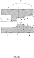
- an interface 10 is provided between an integrated circuit 11 and an energy transmission device 13.
- interface 10 may be provided between a MMIC and a waveguide.
- Interface 10 is configured to be a low-loss interface and comprises a step launch 16 that directly connects circuit 11 to energy transmission device 13 without the use of dielectric materials.
- Interface 10 is configured to match the impedance and mode of energy wave propagation from circuit 11 to energy transmission device 13.
- interface 10 may be formed from two pieces of energy transmission material such as a lid 3 and a package base 5 being connected together.
- lid 3 and base 5 are formed in such a shape that when these two parts are properly aligned they form a cavity that comprises step launch 16 of interface 10 and that further comprises the energy transmission device 13.
- the two housing portions are shaped such that when brought together they form a recess that is interface 10 and waveguide 13 and where interface 10 is a gradual transition to the waveguide cavity.
- interface 10 forms an abrupt mechanical transition from circuit 11 to the waveguide cavity or other energy transmission device 13.
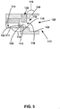
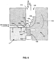
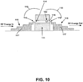
- step launch 115 comprises a single ridge step launch (e.g., steps 130, 132, 134, etc. on one side only). Step launch 115 is configured to provide a stepped transition from the impedance of integrated circuit 111 to the impedance of energy transmission device 113.
- interface 110 comprises double ridge device (e.g. steps 130, 132, 134 etc. on two sides) and may be formed from two pieces of energy transmission material such as a lid 126 and a package base 128 connected together.
- isolation wall 122 isolates the input and output pads (i.e. the input region 114 and output region 116) present on integrated circuit 111 such as a MMIC. Isolating the input region 114 and output region 116 of a MMIC reduces unwanted feedback. This makes for a more stable MMIC or other integrated circuit 111 that will not oscillate.
- isolation wall 122 prevents loss at high frequencies and increases performance.
- turning screw 138 comprises a shaft 140 connected to a head 142.
- Turning screw 138 is adjustable and adjusts the size of interface cavity 118 to create a size that enables interface 110 to have the least amount of loss depending on the particular application that interface 110 is used for.
- turning screw 138 enables the user to tune the impedance matching between interface 110 and integrated circuit 111 at the connection point.
- turning screw 138 may be adjusted until the interface cavity 118 is such that the least amount of loss occurs. Loss is reduced because interface cavity 118 near output region 116 is adjusted to allow the impedance of integrated circuit 111 to most closely match the impedance of cavity 113 at the location of interface cavity 118.
- interface 110 serves as a pathway for various energy waves, such as RF waves and microwaves.
- Interface 110 provides impedance and mode transformation to meet the desired impedances and modes of integrated circuit 111 and energy transmission device 113.
- the impedance of step launch 115 changes with first step 130 and second step 132 (and possibly additional steps 134, 136) to eventually match the impedance and mode of energy wave propagation of energy transmission device 113 on the opposing end of interface 110.
- first step 130 and second step 132 and possibly additional steps 134, 1366
- this disclosure also contemplates changing the size of the opening in the horizontal direction.
- the size of the cavity in step launch 115 may change from end to end by increasing the height, width, diameter, and/or making any other suitable change to the size or volume of the cavity.
- interface 110 is capable of matching the impedance of energy transmission device 113 with little or no signal loss.
- Interface 110 does not require the use of dielectric materials and/or microstrips in one exemplary embodiment. In other exemplary embodiments, some dielectric materials may be used in the manufacture of various components of interface 110.
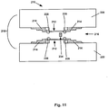
- circuits 212 are integrated circuits such as MMICs. In another example circuits 212 comprise discrete components on a circuit board such as power amplifiers, low noise amplifiers, detectors, limiters, isolators, switches, filters, multiplexers, couplers, and the like. Circuits 212 can be any type of circuit, circuit board, printed circuit board, integrated circuit, discrete component, combination of discrete components, or other type of device or medium that produces, receives, or transfers electronic waves such as microwave signals. As such, the terms "circuit” or "integrated circuit” are not limited to devices with discrete components on a circuit board, but rather include any device that passes energy waves such as antennas, wires, cables, or waveguides.
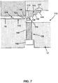
- each step is 0.5 millimeters at Ka band frequencies. At lower frequencies, the height can more significant; for example, a height of 3 millimeters. In other examples however, the depth and/or height of each step may vary compared to one or more other steps in the step launch. Moreover, the corner or edges of steps 232 are rounded to approximately a radius of 0.001 millimeters to 1 millimeter in one exemplary embodiment which further reduces loss.
- isolation wall 234 prevents loss at high frequencies and increases performance.
- pin 226 is any device configured to transport electrical energy from circuits 212 to another destination such as interface 214.
- pin 226 has a coaxial structure with a center conductor and an outer conductor.
- Pin 226 can be constructed from any electrically conductive material.
- pin 226 is constructed from the same material as interface 214 and is gold plated.
- pin 226 is comprised of silver, copper, aluminum, plated plastics, plated ceramics, various metals and/or alloys, and/or other similar materials with low resistance.
- pin 226 is seated or disposed within structure 218 and surrounded by an air channel 236.
- air is not used in air channel 236 and another dielectric is used.
- Certain exemplary dielectrics comprise glass, quartz, foam, or a product such as Teflon® produced by the E. I. DuPont DeNemours and Company of Wilmington, Delaware or other to increase mechanical stability.
- pin 226 further comprises a flange member (not shown) to secure it to lid 220 or base 222. As shown in FIG.
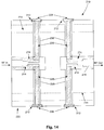
- this section of the multi-level electronic system comprises one or more walls 246 and houses four circuits 212.
- Energy from the splitting level referenced in FIG. 16 is inputted into circuits 212 and amplified. Energy enters and exits circuits 212 through energy transmission devices 216 as shown. After amplification, the energy travels along a waveguide cavity 242 defined by the multi-level electronic system. Energy leaves coupler 238 through energy transmission devices 216 that are wire boned to pin 248 where it is delivered to another section of the multi-level electronic system, such as the section shown in FIG. 16 .
Landscapes
- Engineering & Computer Science (AREA)
- Power Engineering (AREA)
- Microwave Amplifiers (AREA)
Claims (8)
- Système comprenant :un circuit intégré monolithique hyperfréquences (11, 111, 212) comprenant un plot d'entrée, et un plot de sortie, le circuit intégré monolithique hyperfréquences (11, 111, 212) ayant une première impédance ;un guide d'onde (120) ayant une seconde impédance ;une interface (10, 110) ; etune structure (17) entourant le circuit intégré monolithique hyperfréquences (11, 111, 212) et l'interface,dans lequel l'interface comprend :un support de guide d'onde (16, 115) ayant la première impédance à la première extrémité et la seconde impédance à une seconde extrémité, dans lequel la seconde extrémité est reliée au guide d'onde (120) ;une première paroi d'isolation (122) placée au-dessus du circuit intégré monolithique hyperfréquences et située entre le plot d'entrée et le plot de sortie, la première paroi d'isolation faisant partie de la structure (17) entourant le circuit intégré monolithique hyperfréquences (11, 111, 212) et l'interface ; etune cavité (118) définie par le support de guide d'onde (16, 115), dans lequel la cavité a une taille différente en différents points dans la direction d'un trajet de micro-ondes, et dans lequel la taille de la cavité augmente en différents points le long de la direction du trajet de micro-ondes du circuit intégré monolithique hyperfréquences (11, 111, 212) au guide d'onde (26, 120),dans lequel le plot de sortie (116) du circuit intégré monolithique hyperfréquences (11, 111, 212) est relié par un fil (112) soit à la paroi d'isolation (122) soit au support de guide d'onde (16, 115).
- Système selon la revendication 1, dans lequel l'interface (10, 110) comprend en outre une broche qui relie le support de guide d'onde (16, 115) au circuit intégré monolithique hyperfréquences (11, 111, 212).
- Système selon la revendication 1, dans lequel le support de guide d'onde (16, 115) comprend une transition progressive.
- Système selon la revendication 1, dans lequel le support de guide d'onde (16, 115) comprend une transition inclinée.
- Système selon la revendication 1, dans lequel l'interface comprend un élément réglable configuré pour ajuster le volume de la partie de la cavité (119) définie par l'interface.
- Système selon la revendication 5, dans lequel l'élément réglable est une vis (138) en communication avec la cavité qui ajuste le volume de la cavité le long de la partie de la cavité définie par l'interface (110).
- Système selon la revendication 6, dans lequel la vis (138) est située sur un côté opposé de la cavité par rapport à l'interface (110).
- Système selon la revendication 1, dans lequel la première paroi d'isolation se trouve à environ 0,5 à 0,05 millimètre du circuit intégré monolithique hyperfréquence (111) .
Applications Claiming Priority (4)
| Application Number | Priority Date | Filing Date | Title |
|---|---|---|---|
| US11/853,287 US7782156B2 (en) | 2007-09-11 | 2007-09-11 | Low-loss interface |
| US12/039,529 US7812686B2 (en) | 2008-02-28 | 2008-02-28 | Adjustable low-loss interface |
| US3641708P | 2008-03-13 | 2008-03-13 | |
| PCT/US2008/075969 WO2009036134A1 (fr) | 2007-09-11 | 2008-09-11 | Interface à faibles pertes |
Publications (3)
| Publication Number | Publication Date |
|---|---|
| EP2201679A1 EP2201679A1 (fr) | 2010-06-30 |
| EP2201679A4 EP2201679A4 (fr) | 2012-03-21 |
| EP2201679B1 true EP2201679B1 (fr) | 2019-02-20 |
Family
ID=40452468
Family Applications (1)
| Application Number | Title | Priority Date | Filing Date |
|---|---|---|---|
| EP08799446.3A Active EP2201679B1 (fr) | 2007-09-11 | 2008-09-11 | Interface à faibles pertes |
Country Status (2)
| Country | Link |
|---|---|
| EP (1) | EP2201679B1 (fr) |
| WO (1) | WO2009036134A1 (fr) |
Cited By (1)
| Publication number | Priority date | Publication date | Assignee | Title |
|---|---|---|---|---|
| EP4165719A1 (fr) * | 2020-06-11 | 2023-04-19 | Thales | Amplificateur hyperfrequences de puissance a etat solide et combineur de puissance comprenant quatre tels amplificateurs a etat solide |
Families Citing this family (2)
| Publication number | Priority date | Publication date | Assignee | Title |
|---|---|---|---|---|
| US11196383B2 (en) | 2018-06-20 | 2021-12-07 | Telefonaktiebolaget Lm Ericsson (Publ) | Tunable oscillator device |
| FI131875B1 (en) * | 2023-12-11 | 2026-01-21 | Teknologian Tutkimuskeskus Vtt Oy | Amplifier module |
Citations (1)
| Publication number | Priority date | Publication date | Assignee | Title |
|---|---|---|---|---|
| EP0834954A1 (fr) * | 1996-10-01 | 1998-04-08 | Alcatel | Transition entre un guide d'ondes à crête et un circuit planaire |
Family Cites Families (12)
| Publication number | Priority date | Publication date | Assignee | Title |
|---|---|---|---|---|
| DE3127693C2 (de) * | 1981-07-14 | 1985-08-08 | ANT Nachrichtentechnik GmbH, 7150 Backnang | Übergang von einem Hohlleiter auf eine Mikrostreifenleitung |
| US5218373A (en) * | 1990-10-01 | 1993-06-08 | Harris Corporation | Hermetically sealed waffle-wall configured assembly including sidewall and cover radiating elements and a base-sealed waveguide window |
| US5488380A (en) * | 1991-05-24 | 1996-01-30 | The Boeing Company | Packaging architecture for phased arrays |
| US5945894A (en) * | 1995-03-22 | 1999-08-31 | Murata Manufacturing Co., Ltd. | Dielectric resonator and filter utilizing a non-radiative dielectric waveguide device |
| DE19636890C1 (de) * | 1996-09-11 | 1998-02-12 | Bosch Gmbh Robert | Übergang von einem Hohlleiter auf eine Streifenleitung |
| US6363605B1 (en) * | 1999-11-03 | 2002-04-02 | Yi-Chi Shih | Method for fabricating a plurality of non-symmetrical waveguide probes |
| SE518679C2 (sv) * | 2001-03-05 | 2002-11-05 | Saab Ab | Mikrostripövergång |
| US6788171B2 (en) * | 2002-03-05 | 2004-09-07 | Xytrans, Inc. | Millimeter wave (MMW) radio frequency transceiver module and method of forming same |
| US7161422B2 (en) * | 2003-01-03 | 2007-01-09 | Junghyun Kim | Multiple power mode amplifier with bias modulation option and without bypass switches |
| JP2004254223A (ja) * | 2003-02-21 | 2004-09-09 | New Japan Radio Co Ltd | 導波管入出力マイクロ波回路 |
| US7068121B2 (en) * | 2003-06-30 | 2006-06-27 | Tyco Technology Resources | Apparatus for signal transitioning from a device to a waveguide |
| JP4013851B2 (ja) * | 2003-07-17 | 2007-11-28 | 日立電線株式会社 | 導波管平面線路変換装置 |
-
2008
- 2008-09-11 EP EP08799446.3A patent/EP2201679B1/fr active Active
- 2008-09-11 WO PCT/US2008/075969 patent/WO2009036134A1/fr not_active Ceased
Patent Citations (1)
| Publication number | Priority date | Publication date | Assignee | Title |
|---|---|---|---|---|
| EP0834954A1 (fr) * | 1996-10-01 | 1998-04-08 | Alcatel | Transition entre un guide d'ondes à crête et un circuit planaire |
Cited By (1)
| Publication number | Priority date | Publication date | Assignee | Title |
|---|---|---|---|---|
| EP4165719A1 (fr) * | 2020-06-11 | 2023-04-19 | Thales | Amplificateur hyperfrequences de puissance a etat solide et combineur de puissance comprenant quatre tels amplificateurs a etat solide |
Also Published As
| Publication number | Publication date |
|---|---|
| EP2201679A4 (fr) | 2012-03-21 |
| EP2201679A1 (fr) | 2010-06-30 |
| WO2009036134A1 (fr) | 2009-03-19 |
Similar Documents
| Publication | Publication Date | Title |
|---|---|---|
| US7812686B2 (en) | Adjustable low-loss interface | |
| US7782156B2 (en) | Low-loss interface | |
| US9368854B2 (en) | Multi-level power amplification system | |
| US11431294B2 (en) | Antenna waveguide transitions for solid state power amplifiers | |
| US5920240A (en) | High efficiency broadband coaxial power combiner/splitter with radial slotline cards | |
| US7855612B2 (en) | Direct coaxial interface for circuits | |
| US6967543B2 (en) | Microstrip-to-waveguide power combiner for radio frequency power combining | |
| US6828875B2 (en) | Compact slotted-waveguide spatial power divider/combiner/amplifier | |
| US6512431B2 (en) | Millimeterwave module compact interconnect | |
| US5291650A (en) | Method of providing a integrated waveguide combiner | |
| JP2005027299A (ja) | 信号変換装置及び多ポートデバイス | |
| JPH02288501A (ja) | 導波管とマイクロストリップと間の変換装置 | |
| EP2201679B1 (fr) | Interface à faibles pertes | |
| JP2015528672A (ja) | 高次高調波フィルタとして機能するrf電力結合器 | |
| CN113169433B (zh) | 有源波导过渡器和rf信号通信系统 | |
| KR101473647B1 (ko) | 동축도파관 공간결합기 | |
| CN121219911A (zh) | 多层波导过渡部 | |
| JP2022185566A (ja) | 集積ダイプレクサを備えた小型で薄型の開口アンテナ | |
| US8896400B1 (en) | Ultrathin waveguide beamformer | |
| EP0491505B1 (fr) | Combinateur intégré à guides d'ondes | |
| WO2008137477A1 (fr) | Interface coaxiale d'impédance à faible perte pour des circuits intégrés | |
| CN223167636U (zh) | 微带转波导传输装置和通信设备 | |
| KR102425030B1 (ko) | 고출력 방사형 결합기 | |
| CN119153918A (zh) | 微带转波导传输装置和通信设备 | |
| CN120376910A (zh) | 一种具有超宽带性能的微同轴双定向耦合器及其封装结构 |
Legal Events
| Date | Code | Title | Description |
|---|---|---|---|
| PUAI | Public reference made under article 153(3) epc to a published international application that has entered the european phase |
Free format text: ORIGINAL CODE: 0009012 |
|
| 17P | Request for examination filed |
Effective date: 20100409 |
|
| AK | Designated contracting states |
Kind code of ref document: A1 Designated state(s): AT BE BG CH CY CZ DE DK EE ES FI FR GB GR HR HU IE IS IT LI LT LU LV MC MT NL NO PL PT RO SE SI SK TR |
|
| AX | Request for extension of the european patent |
Extension state: AL BA MK RS |
|
| DAX | Request for extension of the european patent (deleted) | ||
| A4 | Supplementary search report drawn up and despatched |
Effective date: 20120216 |
|
| RIC1 | Information provided on ipc code assigned before grant |
Ipc: H01P 5/107 20060101ALI20120210BHEP Ipc: H03F 1/14 20060101AFI20120210BHEP |
|
| 17Q | First examination report despatched |
Effective date: 20130527 |
|
| STAA | Information on the status of an ep patent application or granted ep patent |
Free format text: STATUS: EXAMINATION IS IN PROGRESS |
|
| GRAJ | Information related to disapproval of communication of intention to grant by the applicant or resumption of examination proceedings by the epo deleted |
Free format text: ORIGINAL CODE: EPIDOSDIGR1 |
|
| STAA | Information on the status of an ep patent application or granted ep patent |
Free format text: STATUS: GRANT OF PATENT IS INTENDED |
|
| RIC1 | Information provided on ipc code assigned before grant |
Ipc: H03F 1/14 20060101AFI20180621BHEP Ipc: H03F 3/60 20060101ALI20180621BHEP Ipc: H01P 5/107 20060101ALI20180621BHEP |
|
| GRAP | Despatch of communication of intention to grant a patent |
Free format text: ORIGINAL CODE: EPIDOSNIGR1 |
|
| INTG | Intention to grant announced |
Effective date: 20180730 |
|
| GRAS | Grant fee paid |
Free format text: ORIGINAL CODE: EPIDOSNIGR3 |
|
| GRAJ | Information related to disapproval of communication of intention to grant by the applicant or resumption of examination proceedings by the epo deleted |
Free format text: ORIGINAL CODE: EPIDOSDIGR1 |
|
| GRAL | Information related to payment of fee for publishing/printing deleted |
Free format text: ORIGINAL CODE: EPIDOSDIGR3 |
|
| STAA | Information on the status of an ep patent application or granted ep patent |
Free format text: STATUS: EXAMINATION IS IN PROGRESS |
|
| GRAR | Information related to intention to grant a patent recorded |
Free format text: ORIGINAL CODE: EPIDOSNIGR71 |
|
| STAA | Information on the status of an ep patent application or granted ep patent |
Free format text: STATUS: GRANT OF PATENT IS INTENDED |
|
| GRAA | (expected) grant |
Free format text: ORIGINAL CODE: 0009210 |
|
| STAA | Information on the status of an ep patent application or granted ep patent |
Free format text: STATUS: THE PATENT HAS BEEN GRANTED |
|
| INTC | Intention to grant announced (deleted) | ||
| INTG | Intention to grant announced |
Effective date: 20190109 |
|
| AK | Designated contracting states |
Kind code of ref document: B1 Designated state(s): AT BE BG CH CY CZ DE DK EE ES FI FR GB GR HR HU IE IS IT LI LT LU LV MC MT NL NO PL PT RO SE SI SK TR |
|
| REG | Reference to a national code |
Ref country code: GB Ref legal event code: FG4D |
|
| REG | Reference to a national code |
Ref country code: CH Ref legal event code: EP |
|
| REG | Reference to a national code |
Ref country code: DE Ref legal event code: R096 Ref document number: 602008059052 Country of ref document: DE |
|
| REG | Reference to a national code |
Ref country code: AT Ref legal event code: REF Ref document number: 1099504 Country of ref document: AT Kind code of ref document: T Effective date: 20190315 |
|
| REG | Reference to a national code |
Ref country code: IE Ref legal event code: FG4D |
|
| REG | Reference to a national code |
Ref country code: LT Ref legal event code: MG4D |
|
| REG | Reference to a national code |
Ref country code: NL Ref legal event code: MP Effective date: 20190220 |
|
| PG25 | Lapsed in a contracting state [announced via postgrant information from national office to epo] |
Ref country code: LT Free format text: LAPSE BECAUSE OF FAILURE TO SUBMIT A TRANSLATION OF THE DESCRIPTION OR TO PAY THE FEE WITHIN THE PRESCRIBED TIME-LIMIT Effective date: 20190220 Ref country code: FI Free format text: LAPSE BECAUSE OF FAILURE TO SUBMIT A TRANSLATION OF THE DESCRIPTION OR TO PAY THE FEE WITHIN THE PRESCRIBED TIME-LIMIT Effective date: 20190220 Ref country code: SE Free format text: LAPSE BECAUSE OF FAILURE TO SUBMIT A TRANSLATION OF THE DESCRIPTION OR TO PAY THE FEE WITHIN THE PRESCRIBED TIME-LIMIT Effective date: 20190220 Ref country code: PT Free format text: LAPSE BECAUSE OF FAILURE TO SUBMIT A TRANSLATION OF THE DESCRIPTION OR TO PAY THE FEE WITHIN THE PRESCRIBED TIME-LIMIT Effective date: 20190620 Ref country code: NO Free format text: LAPSE BECAUSE OF FAILURE TO SUBMIT A TRANSLATION OF THE DESCRIPTION OR TO PAY THE FEE WITHIN THE PRESCRIBED TIME-LIMIT Effective date: 20190520 |
|
| PG25 | Lapsed in a contracting state [announced via postgrant information from national office to epo] |
Ref country code: LV Free format text: LAPSE BECAUSE OF FAILURE TO SUBMIT A TRANSLATION OF THE DESCRIPTION OR TO PAY THE FEE WITHIN THE PRESCRIBED TIME-LIMIT Effective date: 20190220 Ref country code: IS Free format text: LAPSE BECAUSE OF FAILURE TO SUBMIT A TRANSLATION OF THE DESCRIPTION OR TO PAY THE FEE WITHIN THE PRESCRIBED TIME-LIMIT Effective date: 20190620 Ref country code: HR Free format text: LAPSE BECAUSE OF FAILURE TO SUBMIT A TRANSLATION OF THE DESCRIPTION OR TO PAY THE FEE WITHIN THE PRESCRIBED TIME-LIMIT Effective date: 20190220 Ref country code: GR Free format text: LAPSE BECAUSE OF FAILURE TO SUBMIT A TRANSLATION OF THE DESCRIPTION OR TO PAY THE FEE WITHIN THE PRESCRIBED TIME-LIMIT Effective date: 20190521 Ref country code: NL Free format text: LAPSE BECAUSE OF FAILURE TO SUBMIT A TRANSLATION OF THE DESCRIPTION OR TO PAY THE FEE WITHIN THE PRESCRIBED TIME-LIMIT Effective date: 20190220 Ref country code: BG Free format text: LAPSE BECAUSE OF FAILURE TO SUBMIT A TRANSLATION OF THE DESCRIPTION OR TO PAY THE FEE WITHIN THE PRESCRIBED TIME-LIMIT Effective date: 20190520 |
|
| REG | Reference to a national code |
Ref country code: AT Ref legal event code: MK05 Ref document number: 1099504 Country of ref document: AT Kind code of ref document: T Effective date: 20190220 |
|
| PG25 | Lapsed in a contracting state [announced via postgrant information from national office to epo] |
Ref country code: ES Free format text: LAPSE BECAUSE OF FAILURE TO SUBMIT A TRANSLATION OF THE DESCRIPTION OR TO PAY THE FEE WITHIN THE PRESCRIBED TIME-LIMIT Effective date: 20190220 Ref country code: CZ Free format text: LAPSE BECAUSE OF FAILURE TO SUBMIT A TRANSLATION OF THE DESCRIPTION OR TO PAY THE FEE WITHIN THE PRESCRIBED TIME-LIMIT Effective date: 20190220 Ref country code: RO Free format text: LAPSE BECAUSE OF FAILURE TO SUBMIT A TRANSLATION OF THE DESCRIPTION OR TO PAY THE FEE WITHIN THE PRESCRIBED TIME-LIMIT Effective date: 20190220 Ref country code: SK Free format text: LAPSE BECAUSE OF FAILURE TO SUBMIT A TRANSLATION OF THE DESCRIPTION OR TO PAY THE FEE WITHIN THE PRESCRIBED TIME-LIMIT Effective date: 20190220 Ref country code: IT Free format text: LAPSE BECAUSE OF FAILURE TO SUBMIT A TRANSLATION OF THE DESCRIPTION OR TO PAY THE FEE WITHIN THE PRESCRIBED TIME-LIMIT Effective date: 20190220 Ref country code: EE Free format text: LAPSE BECAUSE OF FAILURE TO SUBMIT A TRANSLATION OF THE DESCRIPTION OR TO PAY THE FEE WITHIN THE PRESCRIBED TIME-LIMIT Effective date: 20190220 Ref country code: DK Free format text: LAPSE BECAUSE OF FAILURE TO SUBMIT A TRANSLATION OF THE DESCRIPTION OR TO PAY THE FEE WITHIN THE PRESCRIBED TIME-LIMIT Effective date: 20190220 |
|
| REG | Reference to a national code |
Ref country code: DE Ref legal event code: R097 Ref document number: 602008059052 Country of ref document: DE |
|
| PG25 | Lapsed in a contracting state [announced via postgrant information from national office to epo] |
Ref country code: PL Free format text: LAPSE BECAUSE OF FAILURE TO SUBMIT A TRANSLATION OF THE DESCRIPTION OR TO PAY THE FEE WITHIN THE PRESCRIBED TIME-LIMIT Effective date: 20190220 |
|
| PLBE | No opposition filed within time limit |
Free format text: ORIGINAL CODE: 0009261 |
|
| STAA | Information on the status of an ep patent application or granted ep patent |
Free format text: STATUS: NO OPPOSITION FILED WITHIN TIME LIMIT |
|
| PG25 | Lapsed in a contracting state [announced via postgrant information from national office to epo] |
Ref country code: AT Free format text: LAPSE BECAUSE OF FAILURE TO SUBMIT A TRANSLATION OF THE DESCRIPTION OR TO PAY THE FEE WITHIN THE PRESCRIBED TIME-LIMIT Effective date: 20190220 |
|
| 26N | No opposition filed |
Effective date: 20191121 |
|
| PG25 | Lapsed in a contracting state [announced via postgrant information from national office to epo] |
Ref country code: SI Free format text: LAPSE BECAUSE OF FAILURE TO SUBMIT A TRANSLATION OF THE DESCRIPTION OR TO PAY THE FEE WITHIN THE PRESCRIBED TIME-LIMIT Effective date: 20190220 |
|
| PG25 | Lapsed in a contracting state [announced via postgrant information from national office to epo] |
Ref country code: TR Free format text: LAPSE BECAUSE OF FAILURE TO SUBMIT A TRANSLATION OF THE DESCRIPTION OR TO PAY THE FEE WITHIN THE PRESCRIBED TIME-LIMIT Effective date: 20190220 |
|
| PG25 | Lapsed in a contracting state [announced via postgrant information from national office to epo] |
Ref country code: MC Free format text: LAPSE BECAUSE OF FAILURE TO SUBMIT A TRANSLATION OF THE DESCRIPTION OR TO PAY THE FEE WITHIN THE PRESCRIBED TIME-LIMIT Effective date: 20190220 |
|
| REG | Reference to a national code |
Ref country code: CH Ref legal event code: PL |
|
| PG25 | Lapsed in a contracting state [announced via postgrant information from national office to epo] |
Ref country code: LI Free format text: LAPSE BECAUSE OF NON-PAYMENT OF DUE FEES Effective date: 20190930 Ref country code: CH Free format text: LAPSE BECAUSE OF NON-PAYMENT OF DUE FEES Effective date: 20190930 Ref country code: LU Free format text: LAPSE BECAUSE OF NON-PAYMENT OF DUE FEES Effective date: 20190911 |
|
| REG | Reference to a national code |
Ref country code: BE Ref legal event code: MM Effective date: 20190930 |
|
| PG25 | Lapsed in a contracting state [announced via postgrant information from national office to epo] |
Ref country code: BE Free format text: LAPSE BECAUSE OF NON-PAYMENT OF DUE FEES Effective date: 20190930 |
|
| PG25 | Lapsed in a contracting state [announced via postgrant information from national office to epo] |
Ref country code: CY Free format text: LAPSE BECAUSE OF FAILURE TO SUBMIT A TRANSLATION OF THE DESCRIPTION OR TO PAY THE FEE WITHIN THE PRESCRIBED TIME-LIMIT Effective date: 20190220 |
|
| PG25 | Lapsed in a contracting state [announced via postgrant information from national office to epo] |
Ref country code: MT Free format text: LAPSE BECAUSE OF FAILURE TO SUBMIT A TRANSLATION OF THE DESCRIPTION OR TO PAY THE FEE WITHIN THE PRESCRIBED TIME-LIMIT Effective date: 20190220 Ref country code: HU Free format text: LAPSE BECAUSE OF FAILURE TO SUBMIT A TRANSLATION OF THE DESCRIPTION OR TO PAY THE FEE WITHIN THE PRESCRIBED TIME-LIMIT; INVALID AB INITIO Effective date: 20080911 |
|
| P01 | Opt-out of the competence of the unified patent court (upc) registered |
Effective date: 20230529 |
|
| PGFP | Annual fee paid to national office [announced via postgrant information from national office to epo] |
Ref country code: DE Payment date: 20250929 Year of fee payment: 18 |
|
| PGFP | Annual fee paid to national office [announced via postgrant information from national office to epo] |
Ref country code: GB Payment date: 20250929 Year of fee payment: 18 |
|
| PGFP | Annual fee paid to national office [announced via postgrant information from national office to epo] |
Ref country code: FR Payment date: 20250925 Year of fee payment: 18 |
|
| PGFP | Annual fee paid to national office [announced via postgrant information from national office to epo] |
Ref country code: IE Payment date: 20250929 Year of fee payment: 18 |