EP2202804A2 - Procédé de fabrication de cellule solaire CIGSS - Google Patents
Procédé de fabrication de cellule solaire CIGSS Download PDFInfo
- Publication number
- EP2202804A2 EP2202804A2 EP09015528A EP09015528A EP2202804A2 EP 2202804 A2 EP2202804 A2 EP 2202804A2 EP 09015528 A EP09015528 A EP 09015528A EP 09015528 A EP09015528 A EP 09015528A EP 2202804 A2 EP2202804 A2 EP 2202804A2
- Authority
- EP
- European Patent Office
- Prior art keywords
- layer
- light absorbing
- absorbing layer
- sulfur
- electrode layer
- Prior art date
- Legal status (The legal status is an assumption and is not a legal conclusion. Google has not performed a legal analysis and makes no representation as to the accuracy of the status listed.)
- Withdrawn
Links
Images


Classifications
-
- C—CHEMISTRY; METALLURGY
- C23—COATING METALLIC MATERIAL; COATING MATERIAL WITH METALLIC MATERIAL; CHEMICAL SURFACE TREATMENT; DIFFUSION TREATMENT OF METALLIC MATERIAL; COATING BY VACUUM EVAPORATION, BY SPUTTERING, BY ION IMPLANTATION OR BY CHEMICAL VAPOUR DEPOSITION, IN GENERAL; INHIBITING CORROSION OF METALLIC MATERIAL OR INCRUSTATION IN GENERAL
- C23C—COATING METALLIC MATERIAL; COATING MATERIAL WITH METALLIC MATERIAL; SURFACE TREATMENT OF METALLIC MATERIAL BY DIFFUSION INTO THE SURFACE, BY CHEMICAL CONVERSION OR SUBSTITUTION; COATING BY VACUUM EVAPORATION, BY SPUTTERING, BY ION IMPLANTATION OR BY CHEMICAL VAPOUR DEPOSITION, IN GENERAL
- C23C14/00—Coating by vacuum evaporation, by sputtering or by ion implantation of the coating forming material
- C23C14/06—Coating by vacuum evaporation, by sputtering or by ion implantation of the coating forming material characterised by the coating material
- C23C14/14—Metallic material, boron or silicon
-
- H—ELECTRICITY
- H10—SEMICONDUCTOR DEVICES; ELECTRIC SOLID-STATE DEVICES NOT OTHERWISE PROVIDED FOR
- H10F—INORGANIC SEMICONDUCTOR DEVICES SENSITIVE TO INFRARED RADIATION, LIGHT, ELECTROMAGNETIC RADIATION OF SHORTER WAVELENGTH OR CORPUSCULAR RADIATION
- H10F19/00—Integrated devices, or assemblies of multiple devices, comprising at least one photovoltaic cell covered by group H10F10/00, e.g. photovoltaic modules
- H10F19/30—Integrated devices, or assemblies of multiple devices, comprising at least one photovoltaic cell covered by group H10F10/00, e.g. photovoltaic modules comprising thin-film photovoltaic cells
-
- C—CHEMISTRY; METALLURGY
- C23—COATING METALLIC MATERIAL; COATING MATERIAL WITH METALLIC MATERIAL; CHEMICAL SURFACE TREATMENT; DIFFUSION TREATMENT OF METALLIC MATERIAL; COATING BY VACUUM EVAPORATION, BY SPUTTERING, BY ION IMPLANTATION OR BY CHEMICAL VAPOUR DEPOSITION, IN GENERAL; INHIBITING CORROSION OF METALLIC MATERIAL OR INCRUSTATION IN GENERAL
- C23C—COATING METALLIC MATERIAL; COATING MATERIAL WITH METALLIC MATERIAL; SURFACE TREATMENT OF METALLIC MATERIAL BY DIFFUSION INTO THE SURFACE, BY CHEMICAL CONVERSION OR SUBSTITUTION; COATING BY VACUUM EVAPORATION, BY SPUTTERING, BY ION IMPLANTATION OR BY CHEMICAL VAPOUR DEPOSITION, IN GENERAL
- C23C14/00—Coating by vacuum evaporation, by sputtering or by ion implantation of the coating forming material
- C23C14/58—After-treatment
- C23C14/5846—Reactive treatment
- C23C14/5866—Treatment with sulfur, selenium or tellurium
-
- H—ELECTRICITY
- H10—SEMICONDUCTOR DEVICES; ELECTRIC SOLID-STATE DEVICES NOT OTHERWISE PROVIDED FOR
- H10F—INORGANIC SEMICONDUCTOR DEVICES SENSITIVE TO INFRARED RADIATION, LIGHT, ELECTROMAGNETIC RADIATION OF SHORTER WAVELENGTH OR CORPUSCULAR RADIATION
- H10F10/00—Individual photovoltaic cells, e.g. solar cells
- H10F10/10—Individual photovoltaic cells, e.g. solar cells having potential barriers
- H10F10/13—Photovoltaic cells having absorbing layers comprising graded bandgaps
-
- H—ELECTRICITY
- H10—SEMICONDUCTOR DEVICES; ELECTRIC SOLID-STATE DEVICES NOT OTHERWISE PROVIDED FOR
- H10F—INORGANIC SEMICONDUCTOR DEVICES SENSITIVE TO INFRARED RADIATION, LIGHT, ELECTROMAGNETIC RADIATION OF SHORTER WAVELENGTH OR CORPUSCULAR RADIATION
- H10F71/00—Manufacture or treatment of devices covered by this subclass
-
- H—ELECTRICITY
- H10—SEMICONDUCTOR DEVICES; ELECTRIC SOLID-STATE DEVICES NOT OTHERWISE PROVIDED FOR
- H10F—INORGANIC SEMICONDUCTOR DEVICES SENSITIVE TO INFRARED RADIATION, LIGHT, ELECTROMAGNETIC RADIATION OF SHORTER WAVELENGTH OR CORPUSCULAR RADIATION
- H10F77/00—Constructional details of devices covered by this subclass
- H10F77/10—Semiconductor bodies
- H10F77/12—Active materials
- H10F77/126—Active materials comprising only Group I-III-VI chalcopyrite materials, e.g. CuInSe2, CuGaSe2 or CuInGaSe2 [CIGS]
-
- H—ELECTRICITY
- H10—SEMICONDUCTOR DEVICES; ELECTRIC SOLID-STATE DEVICES NOT OTHERWISE PROVIDED FOR
- H10F—INORGANIC SEMICONDUCTOR DEVICES SENSITIVE TO INFRARED RADIATION, LIGHT, ELECTROMAGNETIC RADIATION OF SHORTER WAVELENGTH OR CORPUSCULAR RADIATION
- H10F77/00—Constructional details of devices covered by this subclass
- H10F77/10—Semiconductor bodies
- H10F77/16—Material structures, e.g. crystalline structures, film structures or crystal plane orientations
- H10F77/169—Thin semiconductor films on metallic or insulating substrates
- H10F77/1694—Thin semiconductor films on metallic or insulating substrates the films including Group I-III-VI materials, e.g. CIS or CIGS
-
- Y—GENERAL TAGGING OF NEW TECHNOLOGICAL DEVELOPMENTS; GENERAL TAGGING OF CROSS-SECTIONAL TECHNOLOGIES SPANNING OVER SEVERAL SECTIONS OF THE IPC; TECHNICAL SUBJECTS COVERED BY FORMER USPC CROSS-REFERENCE ART COLLECTIONS [XRACs] AND DIGESTS
- Y02—TECHNOLOGIES OR APPLICATIONS FOR MITIGATION OR ADAPTATION AGAINST CLIMATE CHANGE
- Y02E—REDUCTION OF GREENHOUSE GAS [GHG] EMISSIONS, RELATED TO ENERGY GENERATION, TRANSMISSION OR DISTRIBUTION
- Y02E10/00—Energy generation through renewable energy sources
- Y02E10/50—Photovoltaic [PV] energy
- Y02E10/52—PV systems with concentrators
-
- Y—GENERAL TAGGING OF NEW TECHNOLOGICAL DEVELOPMENTS; GENERAL TAGGING OF CROSS-SECTIONAL TECHNOLOGIES SPANNING OVER SEVERAL SECTIONS OF THE IPC; TECHNICAL SUBJECTS COVERED BY FORMER USPC CROSS-REFERENCE ART COLLECTIONS [XRACs] AND DIGESTS
- Y02—TECHNOLOGIES OR APPLICATIONS FOR MITIGATION OR ADAPTATION AGAINST CLIMATE CHANGE
- Y02E—REDUCTION OF GREENHOUSE GAS [GHG] EMISSIONS, RELATED TO ENERGY GENERATION, TRANSMISSION OR DISTRIBUTION
- Y02E10/00—Energy generation through renewable energy sources
- Y02E10/50—Photovoltaic [PV] energy
- Y02E10/541—CuInSe2 material PV cells
-
- Y—GENERAL TAGGING OF NEW TECHNOLOGICAL DEVELOPMENTS; GENERAL TAGGING OF CROSS-SECTIONAL TECHNOLOGIES SPANNING OVER SEVERAL SECTIONS OF THE IPC; TECHNICAL SUBJECTS COVERED BY FORMER USPC CROSS-REFERENCE ART COLLECTIONS [XRACs] AND DIGESTS
- Y02—TECHNOLOGIES OR APPLICATIONS FOR MITIGATION OR ADAPTATION AGAINST CLIMATE CHANGE
- Y02E—REDUCTION OF GREENHOUSE GAS [GHG] EMISSIONS, RELATED TO ENERGY GENERATION, TRANSMISSION OR DISTRIBUTION
- Y02E10/00—Energy generation through renewable energy sources
- Y02E10/50—Photovoltaic [PV] energy
- Y02E10/544—Solar cells from Group III-V materials
Definitions
- the present invention generally relates to a solar cell and a method of fabricating the same, and more particularly, to a solar cell having improved efficiency.
- Solar cells or photovoltaic cells are essential devices for photovoltaic generation for converting sunlight directly into electrical power and are generally fabricated using a semiconductor having a p-n junction region.
- Eg band-gap energy
- the energy When sunlight with energy greater than the band-gap energy (Eg) of a semiconductor projects onto a solar cell, the energy generates electron-hole pairs on a p-n junction region. Electrons gather in an n-type layer and holes gather in a p-type layer by an electric field generated across the p-n junction region, creating electric power at the p-n junction. When electric charges are applied to opposite terminals of the solar cell, a current will flow.
- Eg band-gap energy
- Embodiments of the present invention provide a solar cell having improved photoelectric conversion efficiency and ensured stability.
- Embodiments of the present invention also provide a method of fabricating a solar cell capable of providing for a concentration gradient of a particular elemental constituent to a light absorbing layer of the solar cell while suppressing side reactions, which may be accompanied with the manufacture of the solar cell.
- a solar cell including a substrate, a back electrode layer formed on the substrate, a light absorbing layer formed on the back electrode layer, and a transparent electrode layer formed on the light absorbing layer, wherein the light absorbing layer is comprised of copper (Cu), gallium (Ga), indium (In), sulfur (S), and selenium (Se) and includes a first concentration region in which concentrations of sulfur (S) gradually decrease in a first direction from the back electrode layer to the light absorbing layer.
- a method of fabricating a solar cell including forming a back electrode layer formed on the substrate, formin g a light absorbing layer on the back electrode layer, and forming a transparent electrode layer on the light absorbing layer, wherein the light absorbing layer includes a first concentration region in which concentrations of sulfur (S) gradually decrease in a first direction from the back electrode layer to the light absorbing layer.
- Exemplary embodiments of the present invention are described herein with reference to cross-section illustrations that are schematic illustrations of idealized embodiments (and intermediate structures) of the present invention. As such, variations from the shapes of the illustrations as a result, for example, of manufacturing techniques and/or tolerances, are to be expected. Thus, exemplary embodiments of the present invention should not be construed as limited to the particular shapes of regions illustrated herein but are to include deviations in shapes that result, for example, from manufacturing.
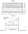
- FIG. 1 is a cross-sectional view of a solar cell according to an exemplary or modified embodiment of the present invention
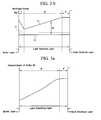
- FIG. 2A illustrates a profile of the band-gap energy of a light absorbing layer in the solar cell shown in FIG. 1 according to the exemplary embodiment of the present invention
- FIG. 2B illustrates a profile of the band-gap energy of a light absorbing layer in the solar cell shown in FIG. 1 according to the modified embodiment of the present invention
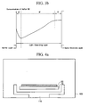
- FIG. 3A illustrates a profile of the concentration of sulfur (S) of the light absorbing layer having the band-gap energy profile illustrated in FIG. 2A according to an embodiment
- FIG. 3B illustrates a profile of the concentration of sulfur (S) of the light absorbing layer having the band-gap energy profile illustrated in FIG. 2B according to an embodiment.
- the solar cell according to an embodiment of the present invention comprises a substrate 10, a back electrode layer 20, a light absorbing layer 30, a buffer layer 40, a window layer 50, a transparent electrode layer 60, and an anti-reflective layer 70.
- soda lime glass may be used as the substrate 10.
- sodium (Na) contained in the soda lime glass substrate 10 may be diffused into the light absorbing layer 30 comprised of a copper (Cu)-indium (In)-gallium (Ga)-sulfur (S)-selenium (Se) (CIGSS) compound, which may increase a charge concentration of the light absorbing layer 30 comprised of the CIGSS compound. This may lead to an increase in the photoelectric conversion efficiency of the solar cell.
- soda lime glass may be advantageously used as the substrate 10.
- alternative usable substrates include but are not limited to ceramics such as alumina, metals such as stainless steel, flexible resins, and the like.
- the back electrode layer 20 allows for movement of charges generated from the light absorbing layer 30 of the solar cell, so that a current flows to the outside of the solar cell.
- the back electrode layer 20 may have high electric conductivity and low specific resistivity. Since the back electrode layer 20 contacts the CIGSS compound forming the light absorbing layer 30, a structure having a low contact resistance value, i.e., an ohmic contact, may be formed between the CIGSS compound ( a P-type semiconductor) and the metallic back electrode layer 20.
- the back electrode layer 20 may maintain stability at a high temperature during heat treatment performed under an atmosphere containing sulfur (S) or selenium (Se), which is accompanied by the forming of the CIGSS compound.
- the back electrode layer 20 may be highly adhesive to the substrate 10.
- the back electrode layer 20 may be made of at least one selected among molybdenum (Mo), gold (Au), aluminum (Al), copper (Cu) and so on.
- Mo molybdenum
- Au gold
- Al aluminum
- Cu copper
- molybdenum (Mo) is a material capable of satisfying the requirements of the back electrode layer 20.
- the light absorbing layer 30 may be comprised of a copper (Cu)-indium (In)-gallium (Ga)-sulfur (S)-selenium (Se) (CIGSS) compound.
- the CIGSS compound is also called a chalcopyrite-based compound, which has p-type semiconductor properties.
- the CIGSS compound semiconductor has a band-gap of a direction transition type of energy.
- the CIGSS compound semiconductor has an optical absorption coefficient of 1x10 5 cm -1 , which is a highest level among semiconductor materials, it is capable of fabricating highly efficient solar cells of a thin film having a thickness of several micrometers. Furthermore, the CIGSS compound exhibits electro optical stability for a prolonged period.
- the light absorbing layer 30 comprises a pentanary compound of copper (Cu), indium (In), gallium (Ga), sulfur (S) and selenium (Se), represented by Cu x (Ga y In 1-y )(S z Se 1-z ) 2 (where 0.75 ⁇ x ⁇ 1, 0.1 ⁇ y ⁇ 0.3, and 0.7 ⁇ z ⁇ 1).
- the Cu x (GayIn 1-y )(S z Se 1-z ) 2 (where 0.75 ⁇ x ⁇ 1, 0.1 ⁇ y ⁇ 0.3, and 0.7 ⁇ z ⁇ 1) compound has a crystalline lattice structure in which indium (In) is replaced partially with gallium (Ga), and elemental sulfur (S) is replaced partially with selenium (Se).
- the band-gap energy of the light absorbing layer 30 will be described with reference to FIG. 2A , in which E v indicates a valence energy band, and Ec indicates a conduction energy band.
- the band-gap energy Eg is an energy gap between the conduction energy band Ec and the valence energy band Ev.
- the band-gap energy Eg near the back electrode layer 20 is high, it makes recombination of electron-hole pairs in a light absorbing layer difficult, thereby improving the efficiency of a solar cell.
- the band-gap energy Eg near the back electrode layer 20 is high, an open circuit voltage Voc of a solar cell may be increased and the efficiency of the solar cell may be improved.
- the open circuit voltage Voc is a potential difference between opposite ends of the solar cell when light is irradiated with infinite impedance applied.
- the open circuit voltage Voc is the maximum voltage that may be obtained from the solar cell. If an open circuit current is much smaller than a short circuit current, the open circuit voltage Voc is generally proportional to the intensity of incident light. In a state in which a p-n junction is formed properly, the higher the band-gap energy of a semiconductor, the greater the open circuit voltage Voc. If the band-gap energy Eg is increased, the current gradually decreases in an open state and the open circuit voltage Voc is increased.
- the band-gap energy Eg may be increased at an interface of the light absorbing layer 30 and the back electrode layer 20, thereby preventing recombination, increasing the open circuit voltage Voc, and finally improving the overall conversion efficiency of the solar cell.
- a region 'A' is a region of the light absorbing layer 30 adjacent to the back electrode layer 20.
- the band-gap energy Eg is highest in the region A.
- a region 'B' is a region of the light absorbing layer 30 extending from the region A away from the back electrode layer 20, into an interior region of the light absorbing layer 30.
- the band-gap energy Eg tends to gradually decrease with distance from the back electrode layer 20.
- the band-gap energy Eg in the region B is smaller than that in the region A, that is, the region of the light absorbing layer 30 adjacent to the back electrode layer 20, in view of photovoltaic effect. If the band-gap energy Eg in the region B is relatively high, like in the region A, electrons are not easily excited from the valence band to the conduction band, lowering the overall conversion efficiency of the solar cell.
- the band-gap energy of the light absorbing layer 30 will be described with reference to FIG. 2B , in which regions A and B are the same as those of FIG. 2A , and a repetitive explanation thereabout will not be given.
- a region 'C' indicates a region of the light absorbing layer 30 adjacent to the buffer layer 40.
- the region C corresponds to an interface between the light absorbing layer 30 and the buffer layer 40 of an n-type semiconductor.
- the band-gap energy Eg in region C may be increased.
- the profile of the band-gap energy Eg in the light absorbing layer 30 may be formed by adjusting the concentration of gallium (Ga).
- the profile of the band-gap energy Eg in the light absorbing layer 30 may be formed by adjusting the concentration of sulfur (S).
- the light absorbing layer 30 is comprised of Cu x (Ga y In 1-y )(S z Se 1-z ) 2 (where 0.75 ⁇ x ⁇ 1, 0.1 ⁇ y ⁇ 0.3, and 0.7 ⁇ z ⁇ 1).
- the y value indicates a proportion of indium (In) partially replaced with gallium (Ga).
- the light absorbing layer 30 includes a first concentration region B' in which the concentrations of sulfur (S) gradually decrease in the first direction from the back electrode layer 20 to the light absorbing layer 30. That is to say, in the Cu x (Ga y In 1-y )(S z Se 1-z ) 2 (where 0.75 ⁇ x ⁇ 1, 0.1 ⁇ y ⁇ 0.3, and 0.7 ⁇ z ⁇ 1) compound of the light absorbing layer 30, values of z gradually decrease in the first direction within the first concentration region B'.
- the profile of the band-gap energy Eg shown in FIG. 2A corresponds to the profile of the concentrations of sulfur (S) shown in FIG. 3A . That is to say, the band-gap energy Eg is generally a smaller value in a region with a smaller concentration of sulfur (S), and vice versa.
- the light absorbing layer 30 according to one or more embodiments of the present invention includes the first concentration region B' in which values of the band-gap energy Eg will gradually decrease in the first direction since the concentrations of sulfur (S) gradually decrease in the first direction. Accordingly, the light absorbing layer 30 in the first concentration region B' allows electrons to be easily excited from the valence band to the conduction band upon absorption of sunlight, thereby improving the overall conversion efficiency of the solar cell.
- the light absorbing layer 30 includes a second concentration region C' in which the concentrations of sulfur (S) gradually increase between the first concentration region B' and the buffer layer 40. That is to say, in the Cu x (GayIn 1-y )(S z Se 1-z ) 2 (where 0.75 ⁇ x ⁇ 1, 0.1 ⁇ y ⁇ 0.3, and 0.7 ⁇ z ⁇ 1) compound of the light absorbing layer 30, values of z gradually increase in the first direction within the second concentration region C'.
- the second concentration region C' of the light absorbing layer 30 has the second concentration region C' in which the concentrations of sulfur (S) gradually increase in the first direction, the band-gap energy Eg gradually increases in the first direction, as shown in FIG. 2B . Accordingly, in the light absorbing layer 30 in the second concentration region B', recombination between excited electrons and holes may be minimized in the light absorbing layer 30, thereby improving the overall conversion efficiency of the solar cell.
- a third concentration region A' corresponds to a region ranging between the first concentration region B' and the back electrode layer 40, in which the concentration of sulfur (S) is constant throughout the entire region.
- the third concentration region A' has a concentration of sulfur (S) that corresponds to the maximum among the concentrations of sulfur (S) of the first and second concentration regions B' and C'.
- the third concentration region A' of the light absorbing layer 30 has a higher concentration of sulfur (S) than the first and second concentration regions B' and C'. Accordingly, the band-gap energy Eg in the third concentration regions A' will be higher than in the first and second concentration regions B' and C'.
- the overall conversion efficiency of the solar cell may also be improved.
- the third concentration region A' corresponds to a first compound layer of the light absorbing layer 30, the first compound layer occupying about 2.5 to 5% of a thickness of the light absorbing layer 30, which will later be described in more detail.
- the first concentration region B', the second concentration region C' and the third concentration region A' representing profiles of concentrations of sulfur (S) correspond to the regions B, C and A of FIG. 2B , respectively. That is to say, the profiles of concentrations of sulfur (S) are substantially the same as the profiles of values of the band-gap energy Eg.
- the buffer layer 40 is positioned on the light absorbing layer 30.
- a pn junction is formed between a CIGSS compound film (i.e., p-type semiconductor) and a ZnO film (i.e., n-type semiconductor).
- a pn junction is formed between the light absorbing layer 30 and the window layer 50 or the transparent electrode layer 60.
- the CIGSS compound and ZnO are quite different from each other in their lattice constants and band-gap energy values.
- the buffer layer 40 may further be provided between the CIGSS compound film and the ZnO film.
- Examples of materials for forming the buffer layer 40 include CdS, ZnS, and the like.
- CdS may be provided according to an embodiment.
- a CdS film is an n-type semiconductor, and the CdS film with a low resistance value may be acquired by doping indium (In), gallium (Ga) or aluminum (Al) into the CdS film.
- the window layer 50 is positioned on the buffer layer 40.
- the window layer 50 is an n-type semiconductor, and forms a pn junction together with the buffer layer 40 and the CIGSS compound.
- the window layer 50 is made of a material having high optical transmission so that sunlight passes through the light absorbing layer 30.
- the window layer 50 may be made of an electrically conducting material so as to function as an electrode layer.
- the window layer 50 may be made of zinc oxide (ZnO), which is an electrically conducting material and has band-gap energy of 3.3 eV and relatively high optical transmission of 80 % or greater.
- the window layer 50 mainly employs intrinsic (non-conductive) i-ZnO without doping of an element of Group III or V of the Periodic Table.
- the transparent electrode layer 60 is positioned on the window layer 50.
- the transparent electrode layer 60 is made of a material having high optical transmission so that sunlight passes through the light absorbing layer 30.
- the transparent electrode layer 60 may be made of a low-resistance, electrically conducting material so as to function as an electrode layer.
- Boron (B) or aluminum (Al) doped ZnO or indium tin oxide (ITO) may be used as the material for forming the transparent electrode layer 60. Since boron (B) or aluminum (Al) doped ZnO has resistance of 10 -4 ⁇ *cm or less, it may be suitably used as an electrode material. In particular, boron (B) doped ZnO increases the optical transmission of light in the near infrared ray region, thereby increasing the open circuit current of the solar cell.
- An anti-reflective layer 70 may further be provided in the transparent electrode layer 60. In order to reduce reflection loss of sunlight incident on the solar cell, the anti-reflective layer 70 is formed on the transparent electrode layer 60, thereby improving the efficiency of the solar cell.
- the anti-reflective layer 70 may be made of MgF 2 .
- FIGS. 1 and 4A through 4I Next, a method of fabricating a solar cell according to the exemplary embodiment of the present invention will be described with reference to FIGS. 1 and 4A through 4I .
- the back electrode layer 20 is formed on the substrate 10.
- the back electrode layer 20 may be made of molybdenum (Mo), which is a material capable of satisfying the requirements of the back electrode layer 20.
- Mo molybdenum
- the back electrode layer 20 may be formed by DC sputtering using a molybdenum (Mo) target.
- the back electrode layer 20 may be formed by chemical vapor deposition (CVD).
- a Cu-Ga layer 31 may be formed on the back electrode layer 20.
- the Cu-Ga layer 31 may be formed by DC sputtering using a Cu-Ga alloy target. Since elemental gallium (Ga) alone is not readily used as a target substance, the Cu-Ga alloy may be used as the target.
- an In layer 32 may be formed on the Cu-Ga layer 31.
- the In layer 32 may be formed by sputtering using an indium (In) target.
- a first precursor consisting of the Cu-Ga layer 31 and the In layer 32 sequentially formed on the back electrode layer 20 may be completed.
- the first precursor may be formed in two steps in the above-described manner.
- the first precursor may also be formed by sputtering using a Cu-Ga-In alloy target.
- the first precursor may be formed by a Cu-Ga-In layer (not shown).
- the first precursor consisting of the Cu-Ga layer 31 and the In layer 32 may be subjected to first heat treatment using a sulfur (S) containing gas 33 to form a first compound layer 34.
- S sulfur
- a chamber 100 for the first heat treatment may be maintained in a vacuum state.
- the S containing gas 33 is introduced into chamber 100.
- the S containing gas 33 may include an inert gas and a hydrogen sulfide (H 2 S) gas.
- H 2 S gas in the sulfur (S) containing gas may have a flow ratio between about 10% and 20%.
- a sufficiently high level of the band-gap energy Eg required at the interface with the back electrode layer 20 may be acquired.
- the first heat treatment may be performed in the chamber 100 maintained at a temperature between about 500 and about 600 °C.
- the first heat treatment may be performed for about 10 to about 30 minutes.
- unreacted materials of the reaction between the first precursor and H 2 S gas may be reduced, and the processing time may also be shortened.
- the first precursor consisting of the Cu-Ga layer 31 and the In layer 32 may be bonded with sulfur (S) to form the first compound layer 34 having a crystalline structure.
- the first compound layer 34 may be finally formed as a part of the light absorbing layer 30 according to one or more embodiments of the present invention in a subsequent process.
- the first compound layer 34 has a considerably high concentration of sulfur (S) based on the profile of the concentrations of sulfur (S) in the finally formed light absorbing layer 30. That is to say, the first compound layer 34 has the third concentration region A' shown in FIGS. 3A and 3B corresponding to the profile of the concentrations of sulfur (S) of the light absorbing layer 30.
- a thickness of the first compound layer 34 may be about 2.5 to 5% of that of the light absorbing layer 30 to be completed in the subsequent process.
- the Cu-Ga layer 35 may be formed on the first compound layer 34.
- an In layer 36 or a Cu-Ga-In layer (not shown) may be formed on the Cu-Ga layer 35.
- the second precursor consisting of the Cu-Ga layer 35 and the In layer 36 may be completed. Since the method of the second precursor is substantially the same as the first precursor, a repetitive explanation thereabout will not be given.
- the first compound layer 34 and the second precursor consisting of the Cu-Ga layer 35 and the In layer 36 may be subjected to a second heat treatment to form the light absorbing layer 30 using a selenium (Se) containing gas 37.
- a selenium (Se) containing gas 37 may be maintained in a vacuum state.
- the Se containing gas 37 is introduced into chamber 100.
- the Se containing gas 37 may include an inert gas and a hydrogen selenide (H 2 Se) gas.
- the H 2 Se gas in the Se containing gas may have a flow ratio between about 3% and 10%. Within the range of the flow ratio stated above, the concentration of Se may be enough to be replaced partially with S in the crystalline lattice structure of the CIGSS compound.
- the second heat treatment may be performed in the chamber 100 maintained at a temperature between about 550 and about 600 °C.
- the second heat treatment may be performed for about 10 to about 60 minutes.
- the second precursor consisting of the first compound, the Cu-Ga layer 35 and the In layer 36 may be bonded with selenium (Se) to form a CIGSS compound layer.
- the thus formed CIGSS compound layer is the light absorbing layer 30 of the solar cell according to one or more embodiments of the present invention. That is to say, the light absorbing layer 30 of the solar cell according to one or more embodiments of the present invention may be a pentanary compound of copper (Cu), indium (In), gallium (Ga), sulfur (S) and selenium (Se), represented by Cu x (Ga y In 1-y )(S z Se 1-z ) 2 (where 0.75 ⁇ x ⁇ 1, 0.1 ⁇ y ⁇ 0.3, and 0.7 ⁇ z ⁇ 1).
- sulfur (S) contained in a higher concentration in the first compound layer than in the second precursor is diffused toward the second precursor. Even if sulfur (S) is diffused from the first compound layer to the second precursor during the second heat treatment, however, the concentrations of sulfur (S) in the first compound layer may be relatively higher than that in the second precursor due to limitation, including a heat treatment time. That is to say, the concentrations of sulfur (S) will gradually decrease from the first compound layer to the second precursor.
- the H 2 Se gas since the H 2 Se gas is introduced upwardly with respect to the second precursor, it may be brought into contact with the second precursor more easily than the first compound layer. Thus, the concentration of selenium (Se) in the second precursor will be higher than that in the first compound layer. Accordingly, in the crystalline lattice structure of the CIGSS compound near the first compound layer, a proportion of selenium (Se) replaced partially with sulfur (S) is decreased during formation of the light absorbing layer 30. On the other hand, near the second precursor, the proportion of selenium (Se) replaced partially with sulfur (S) will be increased. Accordingly, during the second heat treatment, as shown in FIG.
- the concentrations of sulfur (S) in the light absorbing layer 30 will vary by locations of the light absorbing layer 30.
- the light absorbing layer 30 includes the first concentration region B' in which the concentration of sulfur (S) gradually decrease in the first direction from the back electrode layer 20 to the light absorbing layer 30.
- the second heat treatment resulting in the light absorbing layer 30 may be followed by performing a third heat treatment on the light absorbing layer 30 using a sulfur (S) containing gas.
- a sulfur (S) containing gas As a result, the second concentration region C' in which the concentrations of sulfur (S) increase is formed between the buffer layer 40 and the first concentration region B' of the light absorbing layer 30.
- the first compound layer made of the CIGSS compound may be formed at a region between the first concentration region B' of the light absorbing layer 30 and the back electrode layer 20, and the region corresponds to the third concentration region A' in which the concentration of sulfur (S) is relatively higher than in the first and second concentration regions B' and C'. That is to say, the concentration of sulfur (S) is relatively high and the concentration of selenium (Se) is relatively low between the first concentration region B' of the light absorbing layer 30 and the back electrode layer 20, so that the proportion of selenium (Se) replaced with sulfur (S) is relatively reduced in the crystalline lattice structure of the CIGSS compound.
- the concentration of sulfur (S) of the third concentration region A' corresponds to the maximum among concentrations of sulfur (S) of the first and second concentration regions B' and C'.
- the third concentration region A' has substantially the same concentration of sulfur (S) throughout the entire region.
- the profile of the band-gap energy Eg of the light absorbing layer 30 may be formed by forming the profile of the concentration of sulfur (S). Therefore, a highly efficient solar cell having an increased open circuit voltage Voc may be fabricated.
- MoSe 2 which may be formed by a side reaction when the back electrode layer 20 is formed of molybdenum (Mo) during the first heat treatment using a sulfur (S) containing gas. Accordingly, a solar cell may be fabricated, the solar cell having a good crystalline lattice structure in the CIGSS compound while having improved stability.
- the heat treatment for forming the CIGSS compound according to one or more embodiments of the present invention may be carried out at about 550 °C or less.
- the heat treatment for forming the CIGSS compound may be performed at about 550 °C or higher. Accordingly, in consideration of both requirements, an appropriate temperature may be selected and the heat treatment for forming the CIGSS compound may be performed at the selected temperature.
- the formation of MoSe 2 may be minimized using the first compound layer. Therefore, even if heat treatment is performed at 550 °C or higher, since the formation of MoSe 2 is minimized, the heat treatment for forming a CIGSS compound may be performed at 550 °C or higher, thereby forming a CIGSS compound having high-quality crystallinity. In addition, since the formation of MoSe 2 is minimized, deterioration in the adhesion between the back electrode layer 20 and the substrate 10 due to the formation of MoSe 2 may be minimized.
- the buffer layer 40 is formed on the light absorbing layer 30.
- the buffer layer 40 may be formed by a chemical bath deposition (CBD) technique, typically using a CdS based material.
- CBD technique using the CdS based material may be performed in the following manner. First, appropriate amounts of Cd 2+ and S 2- ions were prepared in aqueous solutions. Next, in a case where the product of the respective ion concentrations is greater than the product of solubilities of the respective aqueous solutions, temperatures of the respective aqueous solutions are adjusted, precipitating into CdS, thereby forming the buffer layer 40 that may have a thickness of approximately 50 nm.
- the window layer 50 is formed on the buffer layer 40.
- the transparent electrode layer 60 is formed on the window layer 50.
- the window layer 50 and the transparent electrode layer 60 may be typically made of zinc oxide (ZnO). Accordingly, the window layer 50 and the transparent electrode layer 60 may be formed using any one coating method, including, for example, RF sputtering using a zinc oxide (ZnO) target, spraying, reactive sputtering using a zinc (Zn) target, or metal organic chemical vapor deposition (MOCVD).
- An anti-reflective layer 70 may further be formed on the transparent electrode layer 60.
- the anti-reflective layer 70 may be formed of MgF 2 using an electron-beam physical vapor depositing method.
Landscapes
- Chemical & Material Sciences (AREA)
- Chemical Kinetics & Catalysis (AREA)
- Engineering & Computer Science (AREA)
- Materials Engineering (AREA)
- Mechanical Engineering (AREA)
- Metallurgy (AREA)
- Organic Chemistry (AREA)
- Photovoltaic Devices (AREA)
Applications Claiming Priority (1)
| Application Number | Priority Date | Filing Date | Title |
|---|---|---|---|
| KR1020080132465A KR20100073717A (ko) | 2008-12-23 | 2008-12-23 | 태양전지 및 그 제조 방법 |
Publications (2)
| Publication Number | Publication Date |
|---|---|
| EP2202804A2 true EP2202804A2 (fr) | 2010-06-30 |
| EP2202804A3 EP2202804A3 (fr) | 2014-05-28 |
Family
ID=42224964
Family Applications (1)
| Application Number | Title | Priority Date | Filing Date |
|---|---|---|---|
| EP09015528.4A Withdrawn EP2202804A3 (fr) | 2008-12-23 | 2009-12-16 | Procédé de fabrication de cellule solaire CIGSS |
Country Status (3)
| Country | Link |
|---|---|
| US (1) | US8916767B2 (fr) |
| EP (1) | EP2202804A3 (fr) |
| KR (1) | KR20100073717A (fr) |
Cited By (1)
| Publication number | Priority date | Publication date | Assignee | Title |
|---|---|---|---|---|
| WO2012057490A3 (fr) * | 2010-10-29 | 2012-06-28 | Lg Innotek Co., Ltd. | Appareil à cellules solaires et son procédé de fabrication |
Families Citing this family (23)
| Publication number | Priority date | Publication date | Assignee | Title |
|---|---|---|---|---|
| JP2011018857A (ja) * | 2009-07-10 | 2011-01-27 | Mitsubishi Heavy Ind Ltd | 光電変換装置の製造方法 |
| CN102893410A (zh) * | 2010-04-27 | 2013-01-23 | 京瓷株式会社 | 光电转换装置 |
| US9461186B2 (en) | 2010-07-15 | 2016-10-04 | First Solar, Inc. | Back contact for a photovoltaic module |
| KR101154765B1 (ko) * | 2011-01-19 | 2012-06-18 | 엘지이노텍 주식회사 | 태양전지 및 이의 제조방법 |
| KR101134892B1 (ko) * | 2011-01-24 | 2012-04-13 | 엘지이노텍 주식회사 | 태양전지 및 이의 제조방법 |
| KR101134730B1 (ko) * | 2011-01-25 | 2012-04-19 | 엘지이노텍 주식회사 | 태양전지 및 이의 제조방법 |
| CN103403851A (zh) * | 2011-03-10 | 2013-11-20 | 法国圣戈班玻璃厂 | 制备五元化合物半导体CZTSSe的方法和薄膜太阳能电池 |
| KR101262573B1 (ko) * | 2011-07-29 | 2013-05-08 | 엘지이노텍 주식회사 | 태양전지 및 그의 제조방법 |
| US8436445B2 (en) * | 2011-08-15 | 2013-05-07 | Stion Corporation | Method of manufacture of sodium doped CIGS/CIGSS absorber layers for high efficiency photovoltaic devices |
| CN102956722B (zh) * | 2011-08-19 | 2015-05-27 | 比亚迪股份有限公司 | 一种薄膜太阳能电池 |
| KR101371859B1 (ko) * | 2011-11-11 | 2014-03-10 | 엘지이노텍 주식회사 | 태양전지 및 이의 제조방법 |
| KR101349596B1 (ko) * | 2011-11-25 | 2014-01-10 | 엘지이노텍 주식회사 | 태양전지 및 이의 제조방법 |
| JP5918042B2 (ja) * | 2012-04-10 | 2016-05-18 | 京セラ株式会社 | 光電変換装置の製造方法 |
| KR101349417B1 (ko) * | 2012-04-18 | 2014-01-10 | 엘지이노텍 주식회사 | 태양전지 및 이의 제조방법 |
| US8586457B1 (en) * | 2012-05-17 | 2013-11-19 | Intermolecular, Inc. | Method of fabricating high efficiency CIGS solar cells |
| KR101360548B1 (ko) * | 2012-06-26 | 2014-02-13 | 주식회사 포스코 | 태양전지의 모듈화 방법과 이에 의해 제조된 태양전지 모듈 |
| KR101389832B1 (ko) * | 2012-11-09 | 2014-04-30 | 한국과학기술연구원 | 구리인듐셀레늄(cigs) 또는 구리아연주석황(czts)계 박막형 태양전지 및 그의 제조방법 |
| KR20140066285A (ko) * | 2012-11-22 | 2014-06-02 | 삼성에스디아이 주식회사 | 태양 전지 및 이의 제조 방법 |
| ES2686620T3 (es) * | 2012-12-20 | 2018-10-18 | Saint-Gobain Glass France | Procedimiento para la fabricación de un semiconductor compuesto así como célula solar de capas delgadas |
| US20140261651A1 (en) * | 2013-03-15 | 2014-09-18 | Nanoco Technologies, Ltd. | PV Device with Graded Grain Size and S:Se Ratio |
| JP2014187215A (ja) * | 2013-03-23 | 2014-10-02 | Kyocera Corp | 光電変換装置 |
| US9893220B2 (en) * | 2013-10-15 | 2018-02-13 | Nanoco Technologies Ltd. | CIGS nanoparticle ink formulation having a high crack-free limit |
| CN115458616B (zh) * | 2022-11-14 | 2023-03-10 | 成都中建材光电材料有限公司 | 双面发电玻璃及其制作方法 |
Family Cites Families (9)
| Publication number | Priority date | Publication date | Assignee | Title |
|---|---|---|---|---|
| JP3249408B2 (ja) * | 1996-10-25 | 2002-01-21 | 昭和シェル石油株式会社 | 薄膜太陽電池の薄膜光吸収層の製造方法及び製造装置 |
| JP3249407B2 (ja) * | 1996-10-25 | 2002-01-21 | 昭和シェル石油株式会社 | カルコパイライト系多元化合物半導体薄膜光吸収層からなる薄膜太陽電池 |
| US6323417B1 (en) * | 1998-09-29 | 2001-11-27 | Lockheed Martin Corporation | Method of making I-III-VI semiconductor materials for use in photovoltaic cells |
| US7115304B2 (en) * | 2004-02-19 | 2006-10-03 | Nanosolar, Inc. | High throughput surface treatment on coiled flexible substrates |
| JP2006186200A (ja) | 2004-12-28 | 2006-07-13 | Showa Shell Sekiyu Kk | プリカーサ膜及びその製膜方法 |
| US7442413B2 (en) * | 2005-11-18 | 2008-10-28 | Daystar Technologies, Inc. | Methods and apparatus for treating a work piece with a vaporous element |
| US7632701B2 (en) * | 2006-05-08 | 2009-12-15 | University Of Central Florida Research Foundation, Inc. | Thin film solar cells by selenization sulfurization using diethyl selenium as a selenium precursor |
| US7867551B2 (en) | 2006-09-21 | 2011-01-11 | Solopower, Inc. | Processing method for group IBIIIAVIA semiconductor layer growth |
| WO2008121997A2 (fr) * | 2007-03-30 | 2008-10-09 | Craig Leidholm | Formation de couches d'agent absorbant photovoltaïque sur des substrats en feuille |
-
2008
- 2008-12-23 KR KR1020080132465A patent/KR20100073717A/ko not_active Abandoned
-
2009
- 2009-12-10 US US12/635,660 patent/US8916767B2/en not_active Expired - Fee Related
- 2009-12-16 EP EP09015528.4A patent/EP2202804A3/fr not_active Withdrawn
Non-Patent Citations (1)
| Title |
|---|
| None |
Cited By (3)
| Publication number | Priority date | Publication date | Assignee | Title |
|---|---|---|---|---|
| WO2012057490A3 (fr) * | 2010-10-29 | 2012-06-28 | Lg Innotek Co., Ltd. | Appareil à cellules solaires et son procédé de fabrication |
| CN102782874A (zh) * | 2010-10-29 | 2012-11-14 | Lg伊诺特有限公司 | 太阳能电池设备及其制造方法 |
| CN102782874B (zh) * | 2010-10-29 | 2015-07-29 | Lg伊诺特有限公司 | 太阳能电池设备及其制造方法 |
Also Published As
| Publication number | Publication date |
|---|---|
| US8916767B2 (en) | 2014-12-23 |
| KR20100073717A (ko) | 2010-07-01 |
| US20100154872A1 (en) | 2010-06-24 |
| EP2202804A3 (fr) | 2014-05-28 |
Similar Documents
| Publication | Publication Date | Title |
|---|---|---|
| US8916767B2 (en) | Solar cell and method of fabricating the same | |
| US8193028B2 (en) | Sulfide species treatment of thin film photovoltaic cell and manufacturing method | |
| US5141564A (en) | Mixed ternary heterojunction solar cell | |
| US8198122B2 (en) | Bulk chloride species treatment of thin film photovoltaic cell and manufacturing method | |
| EP1492169A2 (fr) | Cellule solaire | |
| US8008110B1 (en) | Bulk sodium species treatment of thin film photovoltaic cell and manufacturing method | |
| US20070257255A1 (en) | Thin film solar cells by selenization sulfurization using diethyl selenium as a selenium precursor | |
| US9812593B2 (en) | Solar cell and preparing method of the same | |
| US20130104985A1 (en) | Photovoltaic device with mangenese and tellurium interlayer | |
| KR101893411B1 (ko) | 황화아연 버퍼층을 적용한 czts계 박막 태양전지 제조방법 | |
| KR101908475B1 (ko) | 산화막 버퍼층을 포함하는 czts계 박막 태양전지 및 이의 제조방법 | |
| US9935211B2 (en) | Back contact structure for photovoltaic devices such as copper-indium-diselenide solar cells | |
| EP2485272A2 (fr) | Appareil de génération d'énergie solaire et son procédé de fabrication | |
| KR20150142094A (ko) | 원자층 증착법으로 형성된 버퍼층을 포함하는 태양전지 및 이의 제조방법 | |
| EP2738817A2 (fr) | Cellule solaire | |
| KR101036165B1 (ko) | 칼코지나이드계 태양전지의 제조방법 | |
| JP2019071342A (ja) | 薄膜太陽電池の製造方法 | |
| US8435826B1 (en) | Bulk sulfide species treatment of thin film photovoltaic cell and manufacturing method | |
| KR102057234B1 (ko) | Cigs 박막 태양전지의 제조방법 및 이의 방법으로 제조된 cigs 박막 태양전지 | |
| US8394662B1 (en) | Chloride species surface treatment of thin film photovoltaic cell and manufacturing method | |
| KR20170036606A (ko) | 이중 광흡수층을 포함하는 czts계 박막 태양전지 | |
| US20150249171A1 (en) | Method of making photovoltaic device comprising i-iii-vi2 compound absorber having tailored atomic distribution | |
| KR102212042B1 (ko) | 원자층 증착법으로 형성된 버퍼층을 포함하는 태양전지 및 이의 제조방법 | |
| KR102596328B1 (ko) | Czts계 박막 태양전지 광흡수층의 제조방법, 이로부터 제조되는 czts계 박막 태양전지 광흡수층 | |
| US8476104B1 (en) | Sodium species surface treatment of thin film photovoltaic cell and manufacturing method |
Legal Events
| Date | Code | Title | Description |
|---|---|---|---|
| PUAI | Public reference made under article 153(3) epc to a published international application that has entered the european phase |
Free format text: ORIGINAL CODE: 0009012 |
|
| AK | Designated contracting states |
Kind code of ref document: A2 Designated state(s): AT BE BG CH CY CZ DE DK EE ES FI FR GB GR HR HU IE IS IT LI LT LU LV MC MK MT NL NO PL PT RO SE SI SK SM TR |
|
| AX | Request for extension of the european patent |
Extension state: AL BA RS |
|
| RAP1 | Party data changed (applicant data changed or rights of an application transferred) |
Owner name: SAMSUNG SDI CO., LTD. Owner name: SAMSUNG ELECTRONICS CO., LTD. |
|
| RAP1 | Party data changed (applicant data changed or rights of an application transferred) |
Owner name: SAMSUNG ELECTRONICS CO., LTD. Owner name: SAMSUNG SDI CO., LTD. |
|
| PUAL | Search report despatched |
Free format text: ORIGINAL CODE: 0009013 |
|
| AK | Designated contracting states |
Kind code of ref document: A3 Designated state(s): AT BE BG CH CY CZ DE DK EE ES FI FR GB GR HR HU IE IS IT LI LT LU LV MC MK MT NL NO PL PT RO SE SI SK SM TR |
|
| AX | Request for extension of the european patent |
Extension state: AL BA RS |
|
| RIC1 | Information provided on ipc code assigned before grant |
Ipc: C23C 14/06 20060101ALN20140423BHEP Ipc: C23C 14/58 20060101ALN20140423BHEP Ipc: H01L 31/032 20060101AFI20140423BHEP Ipc: H01L 31/18 20060101ALI20140423BHEP Ipc: H01L 31/0392 20060101ALI20140423BHEP Ipc: H01L 31/065 20120101ALI20140423BHEP |
|
| 17P | Request for examination filed |
Effective date: 20141128 |
|
| RBV | Designated contracting states (corrected) |
Designated state(s): AT BE BG CH CY CZ DE DK EE ES FI FR GB GR HR HU IE IS IT LI LT LU LV MC MK MT NL NO PL PT RO SE SI SK SM TR |
|
| RIC1 | Information provided on ipc code assigned before grant |
Ipc: H01L 31/032 20060101AFI20150701BHEP Ipc: H01L 31/18 20060101ALI20150701BHEP Ipc: H01L 31/065 20120101ALI20150701BHEP Ipc: C23C 14/06 20060101ALN20150701BHEP Ipc: H01L 31/0392 20060101ALI20150701BHEP Ipc: C23C 14/58 20060101ALN20150701BHEP |
|
| GRAP | Despatch of communication of intention to grant a patent |
Free format text: ORIGINAL CODE: EPIDOSNIGR1 |
|
| RIC1 | Information provided on ipc code assigned before grant |
Ipc: H01L 31/065 20120101ALI20150825BHEP Ipc: C23C 14/58 20060101ALN20150825BHEP Ipc: H01L 31/032 20060101AFI20150825BHEP Ipc: H01L 31/0392 20060101ALI20150825BHEP Ipc: H01L 31/18 20060101ALI20150825BHEP Ipc: C23C 14/06 20060101ALN20150825BHEP |
|
| RIC1 | Information provided on ipc code assigned before grant |
Ipc: H01L 31/065 20120101ALI20150902BHEP Ipc: H01L 31/18 20060101ALI20150902BHEP Ipc: C23C 14/58 20060101ALN20150902BHEP Ipc: H01L 31/032 20060101AFI20150902BHEP Ipc: H01L 31/0392 20060101ALI20150902BHEP Ipc: C23C 14/06 20060101ALN20150902BHEP |
|
| INTG | Intention to grant announced |
Effective date: 20150915 |
|
| STAA | Information on the status of an ep patent application or granted ep patent |
Free format text: STATUS: THE APPLICATION IS DEEMED TO BE WITHDRAWN |
|
| 18D | Application deemed to be withdrawn |
Effective date: 20160126 |