EP2204860A1 - Herstellung eines Kohlenstoff-passivierten Ovonic-Schwellenschalters - Google Patents
Herstellung eines Kohlenstoff-passivierten Ovonic-Schwellenschalters Download PDFInfo
- Publication number
- EP2204860A1 EP2204860A1 EP09180915A EP09180915A EP2204860A1 EP 2204860 A1 EP2204860 A1 EP 2204860A1 EP 09180915 A EP09180915 A EP 09180915A EP 09180915 A EP09180915 A EP 09180915A EP 2204860 A1 EP2204860 A1 EP 2204860A1
- Authority
- EP
- European Patent Office
- Prior art keywords
- switch
- ovonic threshold
- electrode
- carbon
- ovonic
- Prior art date
- Legal status (The legal status is an assumption and is not a legal conclusion. Google has not performed a legal analysis and makes no representation as to the accuracy of the status listed.)
- Granted
Links
- OKTJSMMVPCPJKN-UHFFFAOYSA-N Carbon Chemical compound [C] OKTJSMMVPCPJKN-UHFFFAOYSA-N 0.000 title claims abstract description 47
- 229910052799 carbon Inorganic materials 0.000 title claims abstract description 47
- 239000003292 glue Substances 0.000 claims abstract description 11
- 239000000463 material Substances 0.000 claims description 28
- 150000004770 chalcogenides Chemical class 0.000 claims description 18
- 238000000034 method Methods 0.000 claims description 9
- NRTOMJZYCJJWKI-UHFFFAOYSA-N Titanium nitride Chemical compound [Ti]#N NRTOMJZYCJJWKI-UHFFFAOYSA-N 0.000 claims description 6
- RTAQQCXQSZGOHL-UHFFFAOYSA-N Titanium Chemical compound [Ti] RTAQQCXQSZGOHL-UHFFFAOYSA-N 0.000 claims description 4
- 150000002500 ions Chemical class 0.000 claims description 4
- 239000010936 titanium Substances 0.000 claims description 4
- 229910052719 titanium Inorganic materials 0.000 claims description 4
- UQZIWOQVLUASCR-UHFFFAOYSA-N alumane;titanium Chemical compound [AlH3].[Ti] UQZIWOQVLUASCR-UHFFFAOYSA-N 0.000 claims description 3
- 238000002156 mixing Methods 0.000 claims description 3
- HBMJWWWQQXIZIP-UHFFFAOYSA-N silicon carbide Chemical compound [Si+]#[C-] HBMJWWWQQXIZIP-UHFFFAOYSA-N 0.000 claims description 2
- 229910010271 silicon carbide Inorganic materials 0.000 claims description 2
- 239000003575 carbonaceous material Substances 0.000 abstract 1
- 239000007772 electrode material Substances 0.000 abstract 1
- 239000010410 layer Substances 0.000 description 32
- 230000001351 cycling effect Effects 0.000 description 6
- 229910052751 metal Inorganic materials 0.000 description 6
- 239000002184 metal Substances 0.000 description 6
- 239000012782 phase change material Substances 0.000 description 6
- 239000011148 porous material Substances 0.000 description 5
- 238000004544 sputter deposition Methods 0.000 description 5
- 230000015556 catabolic process Effects 0.000 description 4
- 238000006731 degradation reaction Methods 0.000 description 4
- 239000011229 interlayer Substances 0.000 description 4
- 150000004767 nitrides Chemical class 0.000 description 4
- RYGMFSIKBFXOCR-UHFFFAOYSA-N Copper Chemical compound [Cu] RYGMFSIKBFXOCR-UHFFFAOYSA-N 0.000 description 3
- 230000004888 barrier function Effects 0.000 description 3
- 229910052802 copper Inorganic materials 0.000 description 3
- 239000010949 copper Substances 0.000 description 3
- 238000000151 deposition Methods 0.000 description 3
- 125000006850 spacer group Chemical group 0.000 description 3
- 239000000758 substrate Substances 0.000 description 3
- XEEYBQQBJWHFJM-UHFFFAOYSA-N Iron Chemical compound [Fe] XEEYBQQBJWHFJM-UHFFFAOYSA-N 0.000 description 2
- 229910052581 Si3N4 Inorganic materials 0.000 description 2
- UGACIEPFGXRWCH-UHFFFAOYSA-N [Si].[Ti] Chemical compound [Si].[Ti] UGACIEPFGXRWCH-UHFFFAOYSA-N 0.000 description 2
- 238000002425 crystallisation Methods 0.000 description 2
- 230000008025 crystallization Effects 0.000 description 2
- 238000005538 encapsulation Methods 0.000 description 2
- 238000005530 etching Methods 0.000 description 2
- -1 i.e. Substances 0.000 description 2
- 238000002161 passivation Methods 0.000 description 2
- 238000000059 patterning Methods 0.000 description 2
- 239000000126 substance Substances 0.000 description 2
- 239000000956 alloy Substances 0.000 description 1
- 229910045601 alloy Inorganic materials 0.000 description 1
- XKRFYHLGVUSROY-UHFFFAOYSA-N argon Substances [Ar] XKRFYHLGVUSROY-UHFFFAOYSA-N 0.000 description 1
- 229910052786 argon Inorganic materials 0.000 description 1
- 229910001423 beryllium ion Inorganic materials 0.000 description 1
- 230000015572 biosynthetic process Effects 0.000 description 1
- 230000001413 cellular effect Effects 0.000 description 1
- 230000007423 decrease Effects 0.000 description 1
- 230000032798 delamination Effects 0.000 description 1
- 230000008021 deposition Effects 0.000 description 1
- 239000003989 dielectric material Substances 0.000 description 1
- 238000009826 distribution Methods 0.000 description 1
- 230000005684 electric field Effects 0.000 description 1
- 238000010849 ion bombardment Methods 0.000 description 1
- 229910052742 iron Inorganic materials 0.000 description 1
- 238000004519 manufacturing process Methods 0.000 description 1
- 238000001465 metallisation Methods 0.000 description 1
- 239000000203 mixture Substances 0.000 description 1
- 230000004044 response Effects 0.000 description 1
- 230000000717 retained effect Effects 0.000 description 1
- 238000005204 segregation Methods 0.000 description 1
- 239000004065 semiconductor Substances 0.000 description 1
- 238000001228 spectrum Methods 0.000 description 1
- 230000003068 static effect Effects 0.000 description 1
Images


Classifications
-
- H—ELECTRICITY
- H10—SEMICONDUCTOR DEVICES; ELECTRIC SOLID-STATE DEVICES NOT OTHERWISE PROVIDED FOR
- H10B—ELECTRONIC MEMORY DEVICES
- H10B63/00—Resistance change memory devices, e.g. resistive RAM [ReRAM] devices
- H10B63/20—Resistance change memory devices, e.g. resistive RAM [ReRAM] devices comprising selection components having two electrodes, e.g. diodes
- H10B63/24—Resistance change memory devices, e.g. resistive RAM [ReRAM] devices comprising selection components having two electrodes, e.g. diodes of the Ovonic threshold switching type
-
- H—ELECTRICITY
- H10—SEMICONDUCTOR DEVICES; ELECTRIC SOLID-STATE DEVICES NOT OTHERWISE PROVIDED FOR
- H10N—ELECTRIC SOLID-STATE DEVICES NOT OTHERWISE PROVIDED FOR
- H10N70/00—Solid-state devices having no potential barriers, and specially adapted for rectifying, amplifying, oscillating or switching
- H10N70/011—Manufacture or treatment of multistable switching devices
- H10N70/041—Modification of switching materials after formation, e.g. doping
-
- H—ELECTRICITY
- H10—SEMICONDUCTOR DEVICES; ELECTRIC SOLID-STATE DEVICES NOT OTHERWISE PROVIDED FOR
- H10N—ELECTRIC SOLID-STATE DEVICES NOT OTHERWISE PROVIDED FOR
- H10N70/00—Solid-state devices having no potential barriers, and specially adapted for rectifying, amplifying, oscillating or switching
- H10N70/011—Manufacture or treatment of multistable switching devices
- H10N70/061—Shaping switching materials
- H10N70/066—Shaping switching materials by filling of openings, e.g. damascene method
-
- H—ELECTRICITY
- H10—SEMICONDUCTOR DEVICES; ELECTRIC SOLID-STATE DEVICES NOT OTHERWISE PROVIDED FOR
- H10N—ELECTRIC SOLID-STATE DEVICES NOT OTHERWISE PROVIDED FOR
- H10N70/00—Solid-state devices having no potential barriers, and specially adapted for rectifying, amplifying, oscillating or switching
- H10N70/20—Multistable switching devices, e.g. memristors
- H10N70/231—Multistable switching devices, e.g. memristors based on solid-state phase change, e.g. between amorphous and crystalline phases, Ovshinsky effect
-
- H—ELECTRICITY
- H10—SEMICONDUCTOR DEVICES; ELECTRIC SOLID-STATE DEVICES NOT OTHERWISE PROVIDED FOR
- H10N—ELECTRIC SOLID-STATE DEVICES NOT OTHERWISE PROVIDED FOR
- H10N70/00—Solid-state devices having no potential barriers, and specially adapted for rectifying, amplifying, oscillating or switching
- H10N70/801—Constructional details of multistable switching devices
- H10N70/821—Device geometry
- H10N70/826—Device geometry adapted for essentially vertical current flow, e.g. sandwich or pillar type devices
-
- H—ELECTRICITY
- H10—SEMICONDUCTOR DEVICES; ELECTRIC SOLID-STATE DEVICES NOT OTHERWISE PROVIDED FOR
- H10N—ELECTRIC SOLID-STATE DEVICES NOT OTHERWISE PROVIDED FOR
- H10N70/00—Solid-state devices having no potential barriers, and specially adapted for rectifying, amplifying, oscillating or switching
- H10N70/801—Constructional details of multistable switching devices
- H10N70/841—Electrodes
- H10N70/8413—Electrodes adapted for resistive heating
-
- H—ELECTRICITY
- H10—SEMICONDUCTOR DEVICES; ELECTRIC SOLID-STATE DEVICES NOT OTHERWISE PROVIDED FOR
- H10N—ELECTRIC SOLID-STATE DEVICES NOT OTHERWISE PROVIDED FOR
- H10N70/00—Solid-state devices having no potential barriers, and specially adapted for rectifying, amplifying, oscillating or switching
- H10N70/801—Constructional details of multistable switching devices
- H10N70/881—Switching materials
- H10N70/882—Compounds of sulfur, selenium or tellurium, e.g. chalcogenides
-
- Y—GENERAL TAGGING OF NEW TECHNOLOGICAL DEVELOPMENTS; GENERAL TAGGING OF CROSS-SECTIONAL TECHNOLOGIES SPANNING OVER SEVERAL SECTIONS OF THE IPC; TECHNICAL SUBJECTS COVERED BY FORMER USPC CROSS-REFERENCE ART COLLECTIONS [XRACs] AND DIGESTS
- Y10—TECHNICAL SUBJECTS COVERED BY FORMER USPC
- Y10S—TECHNICAL SUBJECTS COVERED BY FORMER USPC CROSS-REFERENCE ART COLLECTIONS [XRACs] AND DIGESTS
- Y10S438/00—Semiconductor device manufacturing: process
- Y10S438/90—Bulk effect device making
Definitions
- the present invention relates to a carbon passivated ovonic threshold switch and to a method for forming a carbon passivated ovonic threshold switch.
- Phase change memory devices use phase change materials, i . e ., materials that may be electrically switched between a generally amorphous and a generally crystalline state, for electronic memory application.
- phase change materials i . e ., materials that may be electrically switched between a generally amorphous and a generally crystalline state
- One type of memory element utilizes a phase change material that may be, in one application, electrically switched between a structural state of generally amorphous and generally crystalline local order or between different detectable states of local order across the entire spectrum between completely amorphous and completely crystalline states.
- the state of the phase change material is also non-volatile in that, when set in either a crystalline, semi-crystalline, amorphous, or semi-amorphous state representing a resistance value, that value is retained until changed by another programming event, as that value represents a phase or physical state of the material (e.g., crystalline or amorphous).
- the state is unaffected by removing electrical power.
- the aim of the present invention is to improve endurance reliability of an Ovonic Unified Memory array (threshold voltage distribution) for program cycling stress at different set/reset pulses and for high read cycling.
- an ovonic threshold switch and a method for forming an ovonic threshold switch are provided, as claimed in claims 1 and 8, respectively.
- an ovonic unified memory may be formed with a stacked ovonic threshold switch which is carbon passivated.
- the interface between the middle and upper electrodes to the chalcogenide material forming the ovonic threshold switch may be formed of a relatively thin layer of carbon.
- a glue layer may be used to adhere the carbon layer to the chalcogenide material that forms the ovonic threshold switch.
- An ovonic threshold switch is either on or off depending on the amount of voltage potential applied across the switch and, more particularly, whether the current through the switch exceeds its threshold current or voltage, which then triggers the device into an on state.
- the off state may be substantially electrically non-conductive and the on state may be a substantially conductive state with less resistance than the off state.
- the voltage across the switch in one embodiment, is equal to its holding voltage V hold + IR on , where R on is the dynamic resistance from the extrapolated X axis intercept V hold .
- an ovonic threshold switch may have a threshold voltage V th and, if a voltage potential less than the threshold voltage of the switch is applied across the switch, then the switch may remain off or in a relatively high resistant state so that little or no electrical current passes.
- the device may turn on, i . e ., operate in a relatively low resistance state so that electrical current passes through the switch.
- one or more series connected switches may be in a substantially electrically non-conductive state at less than a predetermined voltage, e.g., the threshold voltage as applied across a switch.
- the switch may be in a substantially conductive state if greater than a predetermined voltage is applied across the switch.
- each switch may comprise a switch material that is a chalcogenide alloy.
- the switch material may be a material in a substantially amorphous state, positioned between two electrodes, that may be repeatedly and reversibly switched between a higher resistance off state that is greater than about 10 megaOhms and a relatively lower resistance on state that is about 1000 Ohms in series with the holding voltage by the application of electrical current or potential.
- Each switch is a two-terminal device that has an IV curve similar to that of a phase change memory element that is in an amorphous state.
- the ovonic threshold switch does not change phase. That is, the switching material of the ovonic threshold switch is not a programmable material and, as a result, the switch may not be a memory device capable of storing information. For example, the switching material may remain permanently amorphous and the IV characteristics may remain the same throughout the operating life.
- the switch In the low voltage, a low electric field mode, where the voltage applied across the switch is less than the threshold voltage V th , the switch may be off or nonconducting and exhibits a relatively high resistance (greater than about 10 megaOhms).
- the switch may remain in the off state until its sufficient voltage, namely, the threshold voltage, is applied or a sufficient current is applied, namely, the threshold current, that switches the device to a conductive relatively low resistance on state.
- the voltage potential across the device After a voltage potential of greater than about the threshold voltage is applied across the device, the voltage potential across the device may drop or snapback to a holding voltage V hold . Snapback may refer to the voltage difference between the threshold voltage and the holding voltage of the switch.
- the voltage potential across the switch may remain close to the holding voltage as current passing through the switch is increased.
- the switch may remain on until the current through the switch drops below a holding current. Below this value, the switch may turn off and return to a relatively high resistance, non-conductive off state, until the threshold voltage and current are again exceeded.
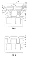
- a phase change memory includes a structure formed over a semiconductor substrate (not indicated in Figure 1 ). Over the substrate there is an interlayer dielectric 10.
- the substrate may include other integrated components which are isolated by the interlayer dielectric 10.
- metal lines 12 are formed in the interlayer dielectric.
- a plug 20 is formed in an intervening nitride layer 14 and oxide layer 16.
- a barrier layer 18 chemically isolates the plug 20.
- the actual memory element is formed in a pair of dielectric layers 22 and 24 in one embodiment.
- Sidewall spacers 28 are formed in a pore that is formed in the dielectric layers 22, 24 and filled with a heater 30 and a phase change material 32, such as a chalcogenide or pnictide in one embodiment.
- the phase change material 32 is an ovonic threshold switch 33.
- the ovonic threshold switch 33 includes a middle electrode 34, a carbon interfacial layer 36, a chalcogenide 38 that normally does not change from the amorphous phase, another carbon interfacial layer 40, and an upper electrode 42. Thereover a metal line 44 is formed, such as a copper column line.
- Figures 2-8 The formation of the structure shown in Figure 1 is illustrated in Figures 2-8 in accordance with one embodiment.
- the interlayer dielectric 10 is patterned and etched to form trenches and metal is deposited in the resulting etched trenches. Then, the metal is planarized to form the metal lines 12.
- the nitride layer 14 is blanket deposited, followed by the oxide layer 16. Other dielectrics may also be used.
- patterning and etching of the resulting stack forms a trench to receive the barrier layer 18, which may be formed of copper, and the plug 20.
- the plug 20 may be formed of titanium nitride or titanium silicon nitride, as two examples.
- the plug material and the barrier layer 18 are planarized to form a planar upper surface, as shown in Figure 3 .
- a lance nitride layer 22 is formed, which is covered by a lance oxide layer 24, as shown in Figure 4 .
- Patterning and etching are used to form pores 26 in the dielectric layers 22, 24, shown in Figure 5 , generally aligned over the plug 20.
- the spacers 28 are formed in the pores using a blanket deposition of a spacer material, such as oxide, followed by an anisotropic etch, as shown in Figure 6 .
- the remaining pore is filled with a heater material, such as titanium silicon nitride, which may initially fill the pore in one embodiment.
- the heater material is then etched back to form the heater 30 and an upper recess which is filled with a phase change material 32, followed by planarization, as shown in Figure 7 .
- the ovonic threshold switch 33 is formed by blanket depositing the middle electrode 34, followed by a glue layer (not shown) and the carbon film 36, followed by the ovonic threshold switch chalcogenide 38, in turn followed by another glue layer (not shown), the carbon film 40, and the top electrode 42.
- the stack is patterned to form a dot, shown in Figure 8 .
- the thickness of the carbon films 36 and 40 is less than or equal to ten percent of the thickness of the associated electrode 34 or 42.
- the carbon films 36 and 40 are formed of amorphous layers formed by sputter depositions. In one embodiment, one or both carbon layers 36 or 40 may be silicon carbide. The films 36 and 40 have thicknesses of from about 5nm to about 10 nm, in one embodiment.
- the films 36 and 40 may include a glue layer to adhere each carbon film 36 or 40 to the chalcogenide 38. Suitable glue layers include titanium, titanium nitride, or titanium aluminum nitride, deposited by sputter deposition.
- the electrodes 34 or 42 may be titanium aluminum nitride or titanium over titanium nitride, in one embodiment.
- the titanium nitride layer in the two layer titanium/titanium nitride film is in contact with the carbon film 36 or 40.
- carbon may be ion mixed into the chalcogenide to form a graded contact.
- the graded carbon contact improves adhesion to the carbon layer in some embodiments.
- Ion mixing is achieved by depositing carbon on the chalcogenide, and then exposing the deposited carbon layer to co-sputtering of carbon.
- the power of carbon and chalcogenide sputtering can be adjusted to control the carbon concentration within the chalcogenide.
- Ion mixing may also be achieved by exposing a deposited carbon layer to high energy ion bombardment.
- the bombardment causes mixture of carbon into the molecular structure of the chalcogenide.
- a graded contact results as the carbon concentration in the chalcogenide decreases with distance from the carbon/chalcogenide interface.
- argon ion accelerated to 300kev is used to bombard thin carbon layers deposited on the chalcogenide.
- Carbon films 36 or 40 of this thickness range may provide good cycling endurance without delamination problems, even if carbon is used without a glue layer, in some embodiments.
- a low temperature nitride encapsulation layer 46 and a high density plasma (HDP) oxide 48 are deposited, as indicated in Figure 1 .
- the deposited encapsulation layer 46 and oxide 48 are planarized using chemical mechanical planarization.
- a mask is used to pattern a via two-way row and another mask is used to pattern the column trenches.
- Metallization and chemical mechanical planarization may follow to complete the via and column.
- Some embodiments may exhibit improved array endurance reliability with set/reset cycling and high read cycling. Degradation may be the result of crystallization and phase segregation of the ovonic threshold material upon thermal/electrical stress. Using carbon passivation, a relatively negligible threshold voltage disturbance and degradation is experienced. After cycling, no crystallization or phase changes may be observed, in some embodiments.
- Figures 9 and 10 are voltage/current plots for repeated switchings of the prior art OTS device and the carbon-passivated OTS device, respectively.
- Figure 9 shows that the repeated switching of the prior art OTS device causes a degradation of the threshold voltage to almost zero. At that point, it is substantially not operating as a switch in that any non-zero voltage produces a substantially flat current response through the OTS device.
- Figure 10 shows that, even with repeated switching, the carbon-passivated device exhibits a well-defined and stable threshold voltage.
- System 500 may be used in wireless devices such as, for example, a personal digital assistant (PDA), a laptop or portable computer with wireless capability, a web tablet, a wireless telephone, a pager, an instant messaging device, a digital music player, a digital camera, or other devices that may be adapted to transmit and/or receive information wirelessly.
- PDA personal digital assistant
- System 500 may be used in any of the following systems: a wireless local area network (WLAN) system, a wireless personal area network (WPAN) system, a cellular network, although the scope of the present invention is not limited in this respect.
- WLAN wireless local area network
- WPAN wireless personal area network
- cellular network although the scope of the present invention is not limited in this respect.
- System 500 may include a controller 510, an input/output (I/O) device 520 (e.g., a keypad, display), static random access memory (SRAM) 560, a memory 530, and a wireless interface 540 coupled to each other via a bus 550.
- I/O input/output
- SRAM static random access memory
- a battery 580 may be used in some embodiments. It should be noted that the scope of the present invention is not limited to embodiments having any or all of these components.
- Controller 510 may comprise, for example, one or more microprocessors, digital signal processors, microcontrollers, or the like.
- Memory 530 may be used to store messages transmitted to or by system 500. Memory 530 may also optionally be used to store instructions that are executed by controller 510 during the operation of system 500, and may be used to store user data.
- Memory 530 may be provided by one or more different types of memory. For example, memory 530 may comprise any type of random access memory, a volatile memory, a non-volatile memory such as a flash memory and/or a memory discussed herein.
- I/O device 520 may be used by a user to generate a message.
- System 500 may use wireless interface 540 to transmit and receive messages to and from a wireless communication network with a radio frequency (RF) signal.
- RF radio frequency
- Examples of wireless interface 540 may include an antenna or a wireless transceiver, although the scope of the present invention is not limited in this respect.
- references throughout this specification to "one embodiment” or “an embodiment” mean that a particular feature, structure, or characteristic described in connection with the embodiment is included in at least one implementation encompassed within the present invention. Thus, appearances of the phrase “one embodiment” or “in an embodiment” are not necessarily referring to the same embodiment. Furthermore, the particular features, structures, or characteristics may be instituted in other suitable forms other than the particular embodiment illustrated and all such forms may be encompassed within the claims of the present application.
Landscapes
- Engineering & Computer Science (AREA)
- Manufacturing & Machinery (AREA)
- Semiconductor Memories (AREA)
- Thermistors And Varistors (AREA)
Applications Claiming Priority (1)
| Application Number | Priority Date | Filing Date | Title |
|---|---|---|---|
| US12/346,705 US7939815B2 (en) | 2008-12-30 | 2008-12-30 | Forming a carbon passivated ovonic threshold switch |
Publications (2)
| Publication Number | Publication Date |
|---|---|
| EP2204860A1 true EP2204860A1 (de) | 2010-07-07 |
| EP2204860B1 EP2204860B1 (de) | 2012-02-08 |
Family
ID=42104564
Family Applications (1)
| Application Number | Title | Priority Date | Filing Date |
|---|---|---|---|
| EP09180915A Not-in-force EP2204860B1 (de) | 2008-12-30 | 2009-12-29 | Herstellung eines Kohlenstoff-passivierten Ovonic-Schwellenschalters |
Country Status (3)
| Country | Link |
|---|---|
| US (1) | US7939815B2 (de) |
| EP (1) | EP2204860B1 (de) |
| AT (1) | ATE545160T1 (de) |
Families Citing this family (23)
| Publication number | Priority date | Publication date | Assignee | Title |
|---|---|---|---|---|
| US8188454B2 (en) * | 2005-10-28 | 2012-05-29 | Ovonyx, Inc. | Forming a phase change memory with an ovonic threshold switch |
| US8377741B2 (en) * | 2008-12-30 | 2013-02-19 | Stmicroelectronics S.R.L. | Self-heating phase change memory cell architecture |
| US8765581B2 (en) | 2009-11-30 | 2014-07-01 | Micron Technology, Inc. | Self-aligned cross-point phase change memory-switch array |
| US8093576B1 (en) * | 2009-11-30 | 2012-01-10 | Micron Technology, Inc. | Chemical-mechanical polish termination layer to build electrical device isolation |
| US8530875B1 (en) * | 2010-05-06 | 2013-09-10 | Micron Technology, Inc. | Phase change memory including ovonic threshold switch with layered electrode and methods for forming same |
| US9166158B2 (en) | 2013-02-25 | 2015-10-20 | Micron Technology, Inc. | Apparatuses including electrodes having a conductive barrier material and methods of forming same |
| CN104518084B (zh) * | 2013-09-29 | 2017-11-03 | 中芯国际集成电路制造(上海)有限公司 | 相变存储器及其形成方法 |
| US10084016B2 (en) | 2013-11-21 | 2018-09-25 | Micron Technology, Inc. | Cross-point memory and methods for fabrication of same |
| US11223014B2 (en) | 2014-02-25 | 2022-01-11 | Micron Technology, Inc. | Semiconductor structures including liners comprising alucone and related methods |
| US9806129B2 (en) | 2014-02-25 | 2017-10-31 | Micron Technology, Inc. | Cross-point memory and methods for fabrication of same |
| US9484196B2 (en) | 2014-02-25 | 2016-11-01 | Micron Technology, Inc. | Semiconductor structures including liners comprising alucone and related methods |
| US9577010B2 (en) | 2014-02-25 | 2017-02-21 | Micron Technology, Inc. | Cross-point memory and methods for fabrication of same |
| US10249819B2 (en) | 2014-04-03 | 2019-04-02 | Micron Technology, Inc. | Methods of forming semiconductor structures including multi-portion liners |
| US9768378B2 (en) | 2014-08-25 | 2017-09-19 | Micron Technology, Inc. | Cross-point memory and methods for fabrication of same |
| US10424619B2 (en) | 2016-01-13 | 2019-09-24 | Samsung Electronics Co., Ltd. | Variable resistance memory devices and methods of manufacturing the same |
| CN108630806A (zh) * | 2017-03-17 | 2018-10-09 | 中芯国际集成电路制造(上海)有限公司 | 相变存储器及其形成方法 |
| KR102375588B1 (ko) * | 2017-07-06 | 2022-03-16 | 삼성전자주식회사 | 반도체 장치 및 그 제조 방법 |
| US11088206B2 (en) * | 2017-10-16 | 2021-08-10 | Sandisk Tehnologies Llc | Methods of forming a phase change memory with vertical cross-point structure |
| US10593875B2 (en) * | 2018-06-15 | 2020-03-17 | Macronix International Co., Ltd. | Self-aligned 3D memory with confined cell |
| US10937832B2 (en) | 2018-06-21 | 2021-03-02 | Macronix International Co., Ltd. | 3D memory with confined cell |
| KR102557911B1 (ko) * | 2018-08-31 | 2023-07-19 | 삼성전자주식회사 | 반도체 장치 및 그 제조 방법 |
| US12249369B2 (en) * | 2021-07-09 | 2025-03-11 | Taiwan Semiconductor Manufacturing Company, Ltd. | Adjusting operation voltage of cross point memory according to aging information |
| CN113871529A (zh) * | 2021-09-29 | 2021-12-31 | 长江先进存储产业创新中心有限责任公司 | 相变存储器及其制造方法 |
Citations (5)
| Publication number | Priority date | Publication date | Assignee | Title |
|---|---|---|---|---|
| EP0269225A2 (de) * | 1986-11-26 | 1988-06-01 | Energy Conversion Devices, Inc. | Elektronische Dünnschichtschaltungen mit Elektroden aus amorphen Kohlenstoff sowie Verfahren zu deren Herstellung |
| US20040114413A1 (en) * | 2002-12-13 | 2004-06-17 | Parkinson Ward D. | Memory and access devices |
| US20040178401A1 (en) * | 2003-03-10 | 2004-09-16 | Ovshinsky Stanford R. | Multi-terminal chalcogenide switching devices |
| EP1677357A1 (de) * | 2004-12-30 | 2006-07-05 | STMicroelectronics S.r.l. | Phasenübergangsspeichereinrichtung mit einer Haftschicht und Herstellungsverfahren dafür |
| US20060261379A1 (en) * | 2005-05-19 | 2006-11-23 | Kabushiki Kaisha Toshiba | Phase change memory and manufacturing method thereof |
Family Cites Families (2)
| Publication number | Priority date | Publication date | Assignee | Title |
|---|---|---|---|---|
| US5159661A (en) * | 1990-10-05 | 1992-10-27 | Energy Conversion Devices, Inc. | Vertically interconnected parallel distributed processor |
| US5414271A (en) * | 1991-01-18 | 1995-05-09 | Energy Conversion Devices, Inc. | Electrically erasable memory elements having improved set resistance stability |
-
2008
- 2008-12-30 US US12/346,705 patent/US7939815B2/en active Active
-
2009
- 2009-12-29 AT AT09180915T patent/ATE545160T1/de active
- 2009-12-29 EP EP09180915A patent/EP2204860B1/de not_active Not-in-force
Patent Citations (5)
| Publication number | Priority date | Publication date | Assignee | Title |
|---|---|---|---|---|
| EP0269225A2 (de) * | 1986-11-26 | 1988-06-01 | Energy Conversion Devices, Inc. | Elektronische Dünnschichtschaltungen mit Elektroden aus amorphen Kohlenstoff sowie Verfahren zu deren Herstellung |
| US20040114413A1 (en) * | 2002-12-13 | 2004-06-17 | Parkinson Ward D. | Memory and access devices |
| US20040178401A1 (en) * | 2003-03-10 | 2004-09-16 | Ovshinsky Stanford R. | Multi-terminal chalcogenide switching devices |
| EP1677357A1 (de) * | 2004-12-30 | 2006-07-05 | STMicroelectronics S.r.l. | Phasenübergangsspeichereinrichtung mit einer Haftschicht und Herstellungsverfahren dafür |
| US20060261379A1 (en) * | 2005-05-19 | 2006-11-23 | Kabushiki Kaisha Toshiba | Phase change memory and manufacturing method thereof |
Also Published As
| Publication number | Publication date |
|---|---|
| EP2204860B1 (de) | 2012-02-08 |
| ATE545160T1 (de) | 2012-02-15 |
| US20100163818A1 (en) | 2010-07-01 |
| US7939815B2 (en) | 2011-05-10 |
Similar Documents
| Publication | Publication Date | Title |
|---|---|---|
| EP2204860B1 (de) | Herstellung eines Kohlenstoff-passivierten Ovonic-Schwellenschalters | |
| US10522757B2 (en) | Dual resistive-material regions for phase change memory devices | |
| US8188454B2 (en) | Forming a phase change memory with an ovonic threshold switch | |
| US7709822B2 (en) | Phase change memory and manufacturing method thereof | |
| US7033856B2 (en) | Spacer chalcogenide memory method | |
| EP1801896B1 (de) | Verfahren zur Herstellung eines Auswahl-Bauelements mit reduziertem Leckstrom, sowie ein Auswahl-Bauelement, insbesondere für Phasenwechsel-Speicher | |
| US7696506B2 (en) | Memory cell with memory material insulation and manufacturing method | |
| CN100562985C (zh) | 制造存储单元的自对准空洞及底电极的方法 | |
| US7531378B2 (en) | Forming an intermediate electrode between an ovonic threshold switch and a chalcogenide memory element | |
| US8101938B2 (en) | Method of forming a chalcogenide memory cell having an ultrasmall cross-sectional area and a chalcogenide memory cell produced by the method | |
| EP1542277A2 (de) | Elektroden für RRAM-Speicherzellen | |
| US20110147695A1 (en) | Fabricating current-confining structures in phase change memory switch cells | |
| US20070279974A1 (en) | Forming heaters for phase change memories with select devices | |
| US7105408B2 (en) | Phase change memory with a select device having a breakdown layer | |
| US9203024B2 (en) | Copper compatible chalcogenide phase change memory with adjustable threshold voltage | |
| US20070018148A1 (en) | Phase change memory with U-shaped chalcogenide cell |
Legal Events
| Date | Code | Title | Description |
|---|---|---|---|
| PUAI | Public reference made under article 153(3) epc to a published international application that has entered the european phase |
Free format text: ORIGINAL CODE: 0009012 |
|
| AK | Designated contracting states |
Kind code of ref document: A1 Designated state(s): AT BE BG CH CY CZ DE DK EE ES FI FR GB GR HR HU IE IS IT LI LT LU LV MC MK MT NL NO PL PT RO SE SI SK SM TR |
|
| AX | Request for extension of the european patent |
Extension state: AL BA RS |
|
| 17P | Request for examination filed |
Effective date: 20110107 |
|
| RIC1 | Information provided on ipc code assigned before grant |
Ipc: H01L 27/24 20060101ALI20110331BHEP Ipc: H01L 45/00 20060101AFI20110331BHEP |
|
| GRAP | Despatch of communication of intention to grant a patent |
Free format text: ORIGINAL CODE: EPIDOSNIGR1 |
|
| GRAS | Grant fee paid |
Free format text: ORIGINAL CODE: EPIDOSNIGR3 |
|
| GRAA | (expected) grant |
Free format text: ORIGINAL CODE: 0009210 |
|
| RAP1 | Party data changed (applicant data changed or rights of an application transferred) |
Owner name: STMICROELECTRONICS SRL |
|
| AK | Designated contracting states |
Kind code of ref document: B1 Designated state(s): AT BE BG CH CY CZ DE DK EE ES FI FR GB GR HR HU IE IS IT LI LT LU LV MC MK MT NL NO PL PT RO SE SI SK SM TR |
|
| REG | Reference to a national code |
Ref country code: GB Ref legal event code: FG4D |
|
| REG | Reference to a national code |
Ref country code: AT Ref legal event code: REF Ref document number: 545160 Country of ref document: AT Kind code of ref document: T Effective date: 20120215 Ref country code: CH Ref legal event code: EP |
|
| REG | Reference to a national code |
Ref country code: DE Ref legal event code: R096 Ref document number: 602009005203 Country of ref document: DE Effective date: 20120405 |
|
| RAP2 | Party data changed (patent owner data changed or rights of a patent transferred) |
Owner name: STMICROELECTRONICS SRL |
|
| REG | Reference to a national code |
Ref country code: NL Ref legal event code: VDEP Effective date: 20120208 |
|
| LTIE | Lt: invalidation of european patent or patent extension |
Effective date: 20120208 |
|
| PG25 | Lapsed in a contracting state [announced via postgrant information from national office to epo] |
Ref country code: HR Free format text: LAPSE BECAUSE OF FAILURE TO SUBMIT A TRANSLATION OF THE DESCRIPTION OR TO PAY THE FEE WITHIN THE PRESCRIBED TIME-LIMIT Effective date: 20120208 Ref country code: NO Free format text: LAPSE BECAUSE OF FAILURE TO SUBMIT A TRANSLATION OF THE DESCRIPTION OR TO PAY THE FEE WITHIN THE PRESCRIBED TIME-LIMIT Effective date: 20120508 Ref country code: LT Free format text: LAPSE BECAUSE OF FAILURE TO SUBMIT A TRANSLATION OF THE DESCRIPTION OR TO PAY THE FEE WITHIN THE PRESCRIBED TIME-LIMIT Effective date: 20120208 Ref country code: NL Free format text: LAPSE BECAUSE OF FAILURE TO SUBMIT A TRANSLATION OF THE DESCRIPTION OR TO PAY THE FEE WITHIN THE PRESCRIBED TIME-LIMIT Effective date: 20120208 Ref country code: IS Free format text: LAPSE BECAUSE OF FAILURE TO SUBMIT A TRANSLATION OF THE DESCRIPTION OR TO PAY THE FEE WITHIN THE PRESCRIBED TIME-LIMIT Effective date: 20120608 |
|
| PG25 | Lapsed in a contracting state [announced via postgrant information from national office to epo] |
Ref country code: GR Free format text: LAPSE BECAUSE OF FAILURE TO SUBMIT A TRANSLATION OF THE DESCRIPTION OR TO PAY THE FEE WITHIN THE PRESCRIBED TIME-LIMIT Effective date: 20120509 Ref country code: LV Free format text: LAPSE BECAUSE OF FAILURE TO SUBMIT A TRANSLATION OF THE DESCRIPTION OR TO PAY THE FEE WITHIN THE PRESCRIBED TIME-LIMIT Effective date: 20120208 Ref country code: PL Free format text: LAPSE BECAUSE OF FAILURE TO SUBMIT A TRANSLATION OF THE DESCRIPTION OR TO PAY THE FEE WITHIN THE PRESCRIBED TIME-LIMIT Effective date: 20120208 Ref country code: PT Free format text: LAPSE BECAUSE OF FAILURE TO SUBMIT A TRANSLATION OF THE DESCRIPTION OR TO PAY THE FEE WITHIN THE PRESCRIBED TIME-LIMIT Effective date: 20120608 Ref country code: FI Free format text: LAPSE BECAUSE OF FAILURE TO SUBMIT A TRANSLATION OF THE DESCRIPTION OR TO PAY THE FEE WITHIN THE PRESCRIBED TIME-LIMIT Effective date: 20120208 Ref country code: BE Free format text: LAPSE BECAUSE OF FAILURE TO SUBMIT A TRANSLATION OF THE DESCRIPTION OR TO PAY THE FEE WITHIN THE PRESCRIBED TIME-LIMIT Effective date: 20120208 |
|
| REG | Reference to a national code |
Ref country code: AT Ref legal event code: MK05 Ref document number: 545160 Country of ref document: AT Kind code of ref document: T Effective date: 20120208 |
|
| PG25 | Lapsed in a contracting state [announced via postgrant information from national office to epo] |
Ref country code: CY Free format text: LAPSE BECAUSE OF FAILURE TO SUBMIT A TRANSLATION OF THE DESCRIPTION OR TO PAY THE FEE WITHIN THE PRESCRIBED TIME-LIMIT Effective date: 20120208 |
|
| PG25 | Lapsed in a contracting state [announced via postgrant information from national office to epo] |
Ref country code: SE Free format text: LAPSE BECAUSE OF FAILURE TO SUBMIT A TRANSLATION OF THE DESCRIPTION OR TO PAY THE FEE WITHIN THE PRESCRIBED TIME-LIMIT Effective date: 20120208 Ref country code: CZ Free format text: LAPSE BECAUSE OF FAILURE TO SUBMIT A TRANSLATION OF THE DESCRIPTION OR TO PAY THE FEE WITHIN THE PRESCRIBED TIME-LIMIT Effective date: 20120208 Ref country code: SI Free format text: LAPSE BECAUSE OF FAILURE TO SUBMIT A TRANSLATION OF THE DESCRIPTION OR TO PAY THE FEE WITHIN THE PRESCRIBED TIME-LIMIT Effective date: 20120208 Ref country code: DK Free format text: LAPSE BECAUSE OF FAILURE TO SUBMIT A TRANSLATION OF THE DESCRIPTION OR TO PAY THE FEE WITHIN THE PRESCRIBED TIME-LIMIT Effective date: 20120208 Ref country code: EE Free format text: LAPSE BECAUSE OF FAILURE TO SUBMIT A TRANSLATION OF THE DESCRIPTION OR TO PAY THE FEE WITHIN THE PRESCRIBED TIME-LIMIT Effective date: 20120208 Ref country code: RO Free format text: LAPSE BECAUSE OF FAILURE TO SUBMIT A TRANSLATION OF THE DESCRIPTION OR TO PAY THE FEE WITHIN THE PRESCRIBED TIME-LIMIT Effective date: 20120208 |
|
| PG25 | Lapsed in a contracting state [announced via postgrant information from national office to epo] |
Ref country code: SK Free format text: LAPSE BECAUSE OF FAILURE TO SUBMIT A TRANSLATION OF THE DESCRIPTION OR TO PAY THE FEE WITHIN THE PRESCRIBED TIME-LIMIT Effective date: 20120208 Ref country code: IT Free format text: LAPSE BECAUSE OF FAILURE TO SUBMIT A TRANSLATION OF THE DESCRIPTION OR TO PAY THE FEE WITHIN THE PRESCRIBED TIME-LIMIT Effective date: 20120208 |
|
| PLBE | No opposition filed within time limit |
Free format text: ORIGINAL CODE: 0009261 |
|
| STAA | Information on the status of an ep patent application or granted ep patent |
Free format text: STATUS: NO OPPOSITION FILED WITHIN TIME LIMIT |
|
| 26N | No opposition filed |
Effective date: 20121109 |
|
| PG25 | Lapsed in a contracting state [announced via postgrant information from national office to epo] |
Ref country code: AT Free format text: LAPSE BECAUSE OF FAILURE TO SUBMIT A TRANSLATION OF THE DESCRIPTION OR TO PAY THE FEE WITHIN THE PRESCRIBED TIME-LIMIT Effective date: 20120208 |
|
| REG | Reference to a national code |
Ref country code: DE Ref legal event code: R097 Ref document number: 602009005203 Country of ref document: DE Effective date: 20121109 |
|
| PG25 | Lapsed in a contracting state [announced via postgrant information from national office to epo] |
Ref country code: ES Free format text: LAPSE BECAUSE OF FAILURE TO SUBMIT A TRANSLATION OF THE DESCRIPTION OR TO PAY THE FEE WITHIN THE PRESCRIBED TIME-LIMIT Effective date: 20120519 |
|
| PG25 | Lapsed in a contracting state [announced via postgrant information from national office to epo] |
Ref country code: BG Free format text: LAPSE BECAUSE OF FAILURE TO SUBMIT A TRANSLATION OF THE DESCRIPTION OR TO PAY THE FEE WITHIN THE PRESCRIBED TIME-LIMIT Effective date: 20120508 Ref country code: MC Free format text: LAPSE BECAUSE OF NON-PAYMENT OF DUE FEES Effective date: 20121231 |
|
| REG | Reference to a national code |
Ref country code: IE Ref legal event code: MM4A |
|
| PG25 | Lapsed in a contracting state [announced via postgrant information from national office to epo] |
Ref country code: IE Free format text: LAPSE BECAUSE OF NON-PAYMENT OF DUE FEES Effective date: 20121229 |
|
| PG25 | Lapsed in a contracting state [announced via postgrant information from national office to epo] |
Ref country code: MT Free format text: LAPSE BECAUSE OF FAILURE TO SUBMIT A TRANSLATION OF THE DESCRIPTION OR TO PAY THE FEE WITHIN THE PRESCRIBED TIME-LIMIT Effective date: 20120208 |
|
| PGFP | Annual fee paid to national office [announced via postgrant information from national office to epo] |
Ref country code: DE Payment date: 20131121 Year of fee payment: 5 |
|
| PG25 | Lapsed in a contracting state [announced via postgrant information from national office to epo] |
Ref country code: TR Free format text: LAPSE BECAUSE OF FAILURE TO SUBMIT A TRANSLATION OF THE DESCRIPTION OR TO PAY THE FEE WITHIN THE PRESCRIBED TIME-LIMIT Effective date: 20120208 |
|
| PG25 | Lapsed in a contracting state [announced via postgrant information from national office to epo] |
Ref country code: LU Free format text: LAPSE BECAUSE OF NON-PAYMENT OF DUE FEES Effective date: 20121229 Ref country code: SM Free format text: LAPSE BECAUSE OF FAILURE TO SUBMIT A TRANSLATION OF THE DESCRIPTION OR TO PAY THE FEE WITHIN THE PRESCRIBED TIME-LIMIT Effective date: 20120208 |
|
| PGFP | Annual fee paid to national office [announced via postgrant information from national office to epo] |
Ref country code: FR Payment date: 20131219 Year of fee payment: 5 |
|
| PG25 | Lapsed in a contracting state [announced via postgrant information from national office to epo] |
Ref country code: HU Free format text: LAPSE BECAUSE OF FAILURE TO SUBMIT A TRANSLATION OF THE DESCRIPTION OR TO PAY THE FEE WITHIN THE PRESCRIBED TIME-LIMIT Effective date: 20091229 |
|
| REG | Reference to a national code |
Ref country code: CH Ref legal event code: PL |
|
| GBPC | Gb: european patent ceased through non-payment of renewal fee |
Effective date: 20131229 |
|
| PG25 | Lapsed in a contracting state [announced via postgrant information from national office to epo] |
Ref country code: CH Free format text: LAPSE BECAUSE OF NON-PAYMENT OF DUE FEES Effective date: 20131231 Ref country code: LI Free format text: LAPSE BECAUSE OF NON-PAYMENT OF DUE FEES Effective date: 20131231 |
|
| PG25 | Lapsed in a contracting state [announced via postgrant information from national office to epo] |
Ref country code: GB Free format text: LAPSE BECAUSE OF NON-PAYMENT OF DUE FEES Effective date: 20131229 |
|
| REG | Reference to a national code |
Ref country code: DE Ref legal event code: R119 Ref document number: 602009005203 Country of ref document: DE |
|
| PG25 | Lapsed in a contracting state [announced via postgrant information from national office to epo] |
Ref country code: MK Free format text: LAPSE BECAUSE OF FAILURE TO SUBMIT A TRANSLATION OF THE DESCRIPTION OR TO PAY THE FEE WITHIN THE PRESCRIBED TIME-LIMIT Effective date: 20120208 |
|
| REG | Reference to a national code |
Ref country code: FR Ref legal event code: ST Effective date: 20150831 |
|
| PG25 | Lapsed in a contracting state [announced via postgrant information from national office to epo] |
Ref country code: DE Free format text: LAPSE BECAUSE OF NON-PAYMENT OF DUE FEES Effective date: 20150701 |
|
| PG25 | Lapsed in a contracting state [announced via postgrant information from national office to epo] |
Ref country code: FR Free format text: LAPSE BECAUSE OF NON-PAYMENT OF DUE FEES Effective date: 20141231 |