EP2207200A1 - Empilement de puces de circuits intégrés enrobées avec des pistes de connexion latérales - Google Patents
Empilement de puces de circuits intégrés enrobées avec des pistes de connexion latérales Download PDFInfo
- Publication number
- EP2207200A1 EP2207200A1 EP20080291240 EP08291240A EP2207200A1 EP 2207200 A1 EP2207200 A1 EP 2207200A1 EP 20080291240 EP20080291240 EP 20080291240 EP 08291240 A EP08291240 A EP 08291240A EP 2207200 A1 EP2207200 A1 EP 2207200A1
- Authority
- EP
- European Patent Office
- Prior art keywords
- stack
- integrated circuit
- face
- electrical connections
- circuit dies
- Prior art date
- Legal status (The legal status is an assumption and is not a legal conclusion. Google has not performed a legal analysis and makes no representation as to the accuracy of the status listed.)
- Ceased
Links
Images


Classifications
-
- H—ELECTRICITY
- H10—SEMICONDUCTOR DEVICES; ELECTRIC SOLID-STATE DEVICES NOT OTHERWISE PROVIDED FOR
- H10W—GENERIC PACKAGES, INTERCONNECTIONS, CONNECTORS OR OTHER CONSTRUCTIONAL DETAILS OF DEVICES COVERED BY CLASS H10
- H10W70/00—Package substrates; Interposers; Redistribution layers [RDL]
- H10W70/01—Manufacture or treatment
- H10W70/05—Manufacture or treatment of insulating or insulated package substrates, or of interposers, or of redistribution layers
- H10W70/08—Manufacture or treatment of insulating or insulated package substrates, or of interposers, or of redistribution layers by depositing layers on the chip or wafer, e.g. "chip-first" RDLs
- H10W70/09—Manufacture or treatment of insulating or insulated package substrates, or of interposers, or of redistribution layers by depositing layers on the chip or wafer, e.g. "chip-first" RDLs extending onto an encapsulation that laterally surrounds the chip or wafer, e.g. fan-out wafer level package [FOWLP] RDLs
-
- H—ELECTRICITY
- H10—SEMICONDUCTOR DEVICES; ELECTRIC SOLID-STATE DEVICES NOT OTHERWISE PROVIDED FOR
- H10W—GENERIC PACKAGES, INTERCONNECTIONS, CONNECTORS OR OTHER CONSTRUCTIONAL DETAILS OF DEVICES COVERED BY CLASS H10
- H10W72/00—Interconnections or connectors in packages
- H10W72/01—Manufacture or treatment
- H10W72/0198—Manufacture or treatment batch processes
-
- H—ELECTRICITY
- H10—SEMICONDUCTOR DEVICES; ELECTRIC SOLID-STATE DEVICES NOT OTHERWISE PROVIDED FOR
- H10W—GENERIC PACKAGES, INTERCONNECTIONS, CONNECTORS OR OTHER CONSTRUCTIONAL DETAILS OF DEVICES COVERED BY CLASS H10
- H10W90/00—Package configurations
-
- H—ELECTRICITY
- H10—SEMICONDUCTOR DEVICES; ELECTRIC SOLID-STATE DEVICES NOT OTHERWISE PROVIDED FOR
- H10W—GENERIC PACKAGES, INTERCONNECTIONS, CONNECTORS OR OTHER CONSTRUCTIONAL DETAILS OF DEVICES COVERED BY CLASS H10
- H10W70/00—Package substrates; Interposers; Redistribution layers [RDL]
- H10W70/60—Insulating or insulated package substrates; Interposers; Redistribution layers
-
- H—ELECTRICITY
- H10—SEMICONDUCTOR DEVICES; ELECTRIC SOLID-STATE DEVICES NOT OTHERWISE PROVIDED FOR
- H10W—GENERIC PACKAGES, INTERCONNECTIONS, CONNECTORS OR OTHER CONSTRUCTIONAL DETAILS OF DEVICES COVERED BY CLASS H10
- H10W72/00—Interconnections or connectors in packages
- H10W72/20—Bump connectors, e.g. solder bumps or copper pillars; Dummy bumps; Thermal bumps
- H10W72/241—Dispositions, e.g. layouts
-
- H—ELECTRICITY
- H10—SEMICONDUCTOR DEVICES; ELECTRIC SOLID-STATE DEVICES NOT OTHERWISE PROVIDED FOR
- H10W—GENERIC PACKAGES, INTERCONNECTIONS, CONNECTORS OR OTHER CONSTRUCTIONAL DETAILS OF DEVICES COVERED BY CLASS H10
- H10W72/00—Interconnections or connectors in packages
- H10W72/801—Interconnections on sidewalls of containers
-
- H—ELECTRICITY
- H10—SEMICONDUCTOR DEVICES; ELECTRIC SOLID-STATE DEVICES NOT OTHERWISE PROVIDED FOR
- H10W—GENERIC PACKAGES, INTERCONNECTIONS, CONNECTORS OR OTHER CONSTRUCTIONAL DETAILS OF DEVICES COVERED BY CLASS H10
- H10W72/00—Interconnections or connectors in packages
- H10W72/90—Bond pads, in general
- H10W72/941—Dispositions of bond pads
- H10W72/9413—Dispositions of bond pads on encapsulations
-
- H—ELECTRICITY
- H10—SEMICONDUCTOR DEVICES; ELECTRIC SOLID-STATE DEVICES NOT OTHERWISE PROVIDED FOR
- H10W—GENERIC PACKAGES, INTERCONNECTIONS, CONNECTORS OR OTHER CONSTRUCTIONAL DETAILS OF DEVICES COVERED BY CLASS H10
- H10W74/00—Encapsulations, e.g. protective coatings
-
- H—ELECTRICITY
- H10—SEMICONDUCTOR DEVICES; ELECTRIC SOLID-STATE DEVICES NOT OTHERWISE PROVIDED FOR
- H10W—GENERIC PACKAGES, INTERCONNECTIONS, CONNECTORS OR OTHER CONSTRUCTIONAL DETAILS OF DEVICES COVERED BY CLASS H10
- H10W74/00—Encapsulations, e.g. protective coatings
- H10W74/01—Manufacture or treatment
- H10W74/019—Manufacture or treatment using temporary auxiliary substrates
-
- H—ELECTRICITY
- H10—SEMICONDUCTOR DEVICES; ELECTRIC SOLID-STATE DEVICES NOT OTHERWISE PROVIDED FOR
- H10W—GENERIC PACKAGES, INTERCONNECTIONS, CONNECTORS OR OTHER CONSTRUCTIONAL DETAILS OF DEVICES COVERED BY CLASS H10
- H10W90/00—Package configurations
- H10W90/10—Configurations of laterally-adjacent chips
Definitions
- the invention relates to forming electrical connections on integrated circuit packages, and in particular to methods of providing electroless metal plated connections on 3-dimensional stacks of integrated circuit packages.
- Integrated circuits are most commonly manufactured by techniques that rely on successive 2-dimensional patterning processes, resulting in integrated circuit (IC) dies.
- the dies are packaged, typically in a mouldable composition such as an epoxy resin, to protect the sensitive components from external environments in use. This process results in integrated circuit chips having a largely planar construction.
- Stacking techniques may be used to increase the density of chips in a given volume, for example by stacking circuit boards on which the chips are mounted.
- each stack of dies is typically required to be cut from a stack of wafers each of which is made up of a 2-dimensional array of dies. This cutting process prevents electrical connections from being made between the dies to a base layer of the stack (e.g. for connection to a motherboard via a BGA) until after the stacks are divided from the stack of wafers.
- a method is therefore required to allow electrical connections to be made along one or more side faces of the stacks after division.
- Advantages of forming 3-dimensional stacks of IC dies in a single package include the absence of the need for wire bonds and the capability of different die sizes to be stacked internally while retaining a similar outer appearance and electrical layout.
- the electrical layout of a stack can be routed via one or more side walls of the package.
- a technique of applying electrical connection traces along the side faces of the stack is required.
- Various techniques may be possible, one of which is that of electroless metal plating, being a well-known technique for depositing conductive metallic coatings on non-conductive, as well as conductive, substrates.
- This plating technique can be used to apply electrical connections on a 3-dimensional stack by applying an overall metallic coating followed by a patterning technique such as laser patterning to form individual traces.
- Laser patterning is, however, problematic due to i) being expensive; ii) tending to result in peeling of the deposited metallic layer; and iii) penetration of the laser into the intermediate layers of the stack (e.g. glue or foil layers), causing defects.
- a method of forming electrical connections on an integrated circuit package comprising:
- the invention overcomes the problems associated with laser machining.
- a finer pitch is possible by using a sawing process, and the invention has the further advantage that the same or similar equipment can be used for package singulation (i.e. dividing the stacks from a stacked wafer package) as for the metal patterning process.
- an integrated circuit package comprising a cuboid-shaped stack within which are moulded a plurality of integrated circuit dies, the stack having a lower face with a plurality of electrical connections provided thereon, a plurality of tracks being provided along a side face of the stack to connect the plurality of electrical connections with each of the plurality of integrated circuit dies, each track separated from adjacent tracks by a groove extending between an upper face and the lower face of the stack.
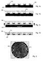
- FIGS 1a to 1d illustrate an exemplary process for obtaining a wafer-scale chip package.
- individual semiconductor dies (or chips) 110 are placed on a carrier substrate 120, the chips being attached to the carrier substrate 120 by means of an temporary bonding layer, for example in the form of a double-side adhesive tape 130.
- an temporary bonding layer for example in the form of a double-side adhesive tape 130.
- each die is tested before being placed on the carrier substrate 120, so that only functioning dies are used.
- the dies 110 are moulded into a wafer 150 by applying a moulding compound 140 around the dies.
- the underside of each die 110, on which electrical connections are to be made, is protected from the moulding compound 140 by being attached to the carrier substrate 120.
- FIG. 1c A plan view of an exemplary wafer 150, in which a 2-dimensional array of dies 110 is embedded, is shown in figure 2 .
- Figures 3a and 3b illustrate schematically a subsequent step performed on each wafer, which provides fan-out electrical connection traces from each die 110. Electrical connections between adjacent dies 310a, 310b are deposited on a surface of the wafer 150, one such connection 320 being shown in figure 3b . Each connection 320 connects a die pad 330 of one die 310a to that of another die 310b. These connections 320 are also shown in cross-section in figure 4a , which illustrates the wafer 150 now attached to a carrier substrate 420 with the exposed surfaces on the dies 310 face-up to allow the connections 320 to be applied. The wafer 150 is then separated from the carrier substrate 420 after the connections are applied ( figure 4b ).
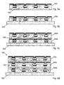
- FIGs 5a to 5d illustrate further processing stages involved in creating a 3-dimensional stack of wafers.
- a glue layer 510 is applied to a face of each wafer 150.
- a first wafer 150a is attached to a carrier substrate 520 ( figure 5b ).
- a second wafer 150b is then attached to the first wafer 150a with the glue layer 510 ( figure 5c ).
- the process is repeated ( figure 5d ) until sufficient layers have been assembled.
- a 3-dimensional stack 530 is then formed in which each layer 150a, 150b, 150c comprises a 2-dimensional array of dies that are electrically connected within the plane of the layer but the layers are electrically isolated from each other by the compound moulding material 140 and glue layers 510.
- the 3-dimensional stack 530 in this case comprising four wafer layers, is then divided into individual stacks 630a-d in a machining operation.
- the machining operation preferably comprises a series of sawing operations, for example using a computer-controlled grinding disc to accurately saw through the wafers between adjacent dies. This machining operation exposes electrical connections 650 on side faces of each of the stacks 630a-d.
- the individual stacks 630a-d can then be removed from the carrier substrate 520.
- FIGS. 7a to 7c illustrate schematically a subsequent series of processing steps to form electrical connections between each layer of the individual stacks 630.
- the stacks 630 are first subjected to an electroless metal plating process, which deposits a metallic layer 710 over at least one side face 640 of the stack 630. This process may be performed while the stacks 630a-d are on the carrier substrate 520, so that electrical output connections on the lower face 650 of each stack are protected.
- a particular preferred material for use as the deposited metal layer 710 is a nickel and gold composition (Ni-Au).
- Ni-Au nickel and gold composition
- Various processes for electroless metal deposition are known in the art, and need not be described here in detail. Further information regarding an exemplary electroless Ni plating process suitable for use with the invention is disclosed by W. Riedel in "Electroless Nickel Plating", ASM International, 1991.
- portions of the metallic layer 710 are selectively removed from the side face 640 of the stack 630 by means of a sawing operation ( figure 7b ).
- a rotating grinding disc 720 may be used to machine narrow grooves 730 along the side face 640 of the stack, forming a plurality of conductive tracks 740 along the side face.
- the remaining metallic layer now in the form of conductive tracks extending between an upper surface and the lower surface 650 of the stack 630, connects with the electrical connections 320 ( figure 4a ) provided on each layer of the stack, so that a connection can be made from the lower face 650 of the stack 630 to each of the individual dies in the stack ( figure 7c ).
- a positioning precision of around 7 ⁇ m is currently possible for the selective sawing step, allowing conductive tracks with a pitch of the order of 25 ⁇ m to be produced.
- the selective sawing process results in several advantages over other techniques such as laser patterning. Firstly, the same equipment can be used that may already be in place for dividing the packages from a stack of wafers, therefore requiring only minor reconfigurations in the process line. Secondly, fine machining by sawing is a well known and mature processing technique, and can achieve high levels of accuracy with low set-up costs as compared with laser machining. Thirdly, sawing can result in a finer scale pitch, and with less resulting surface and sub-surface damage, than laser machining.
- the finished form of a stack 630 is shown schematically in figure 8 , as attached to a printed circuit board (PCB) by a ball grid array 810.
- the lower face 650 of the stack 630 provides the electrical connections to the PCB via a ball grid array 810.
- a redistribution layer 820 on the lower face 630 of the stack allows for appropriate connections on the lower surface to be made to one or more of the side faces 640, on which are provided the conductive tracks 740 resulting from the preceding stages.
- each layer of the stack 630 which may be provided with different fan-out connections to connect with different conductive tracks along one or more side faces of the stack, can be addressed through the connections provided on the lower face 650.
Landscapes
- Internal Circuitry In Semiconductor Integrated Circuit Devices (AREA)
Priority Applications (1)
| Application Number | Priority Date | Filing Date | Title |
|---|---|---|---|
| EP20080291240 EP2207200A1 (fr) | 2008-12-24 | 2008-12-24 | Empilement de puces de circuits intégrés enrobées avec des pistes de connexion latérales |
Applications Claiming Priority (1)
| Application Number | Priority Date | Filing Date | Title |
|---|---|---|---|
| EP20080291240 EP2207200A1 (fr) | 2008-12-24 | 2008-12-24 | Empilement de puces de circuits intégrés enrobées avec des pistes de connexion latérales |
Publications (1)
| Publication Number | Publication Date |
|---|---|
| EP2207200A1 true EP2207200A1 (fr) | 2010-07-14 |
Family
ID=40677758
Family Applications (1)
| Application Number | Title | Priority Date | Filing Date |
|---|---|---|---|
| EP20080291240 Ceased EP2207200A1 (fr) | 2008-12-24 | 2008-12-24 | Empilement de puces de circuits intégrés enrobées avec des pistes de connexion latérales |
Country Status (1)
| Country | Link |
|---|---|
| EP (1) | EP2207200A1 (fr) |
Cited By (3)
| Publication number | Priority date | Publication date | Assignee | Title |
|---|---|---|---|---|
| CN109801850A (zh) * | 2017-11-17 | 2019-05-24 | 英飞凌科技股份有限公司 | 用非电式镀覆法在封装模制体中形成导电连接迹线 |
| US10607955B2 (en) | 2017-06-20 | 2020-03-31 | Sandisk Semiconductor (Shanghai) Co. Ltd. | Heterogeneous fan-out structures for memory devices |
| CN117293057A (zh) * | 2023-09-27 | 2023-12-26 | 山西高科华杰光电科技有限公司 | 一种显示面板封装系统及工艺 |
Citations (6)
| Publication number | Priority date | Publication date | Assignee | Title |
|---|---|---|---|---|
| US5547906A (en) * | 1992-09-14 | 1996-08-20 | Badehi; Pierre | Methods for producing integrated circuit devices |
| WO2001045172A1 (fr) * | 1999-12-15 | 2001-06-21 | 3D Plus | Procede et dispositif d'interconnexion en trois dimensions de composants electroniques |
| US20030047353A1 (en) * | 2001-09-07 | 2003-03-13 | Yamaguchi James Satsuo | Multilayer modules with flexible substrates |
| US20060055039A1 (en) * | 2002-02-07 | 2006-03-16 | Floyd Eide | Stackable layer containing ball grid array package |
| FR2895568A1 (fr) * | 2005-12-23 | 2007-06-29 | 3D Plus Sa Sa | Procede de fabrication collective de modules electroniques 3d |
| US20070158805A1 (en) * | 2002-04-22 | 2007-07-12 | Gann Keith | BGA-scale stacks comprised of layers containing integrated circuit die and a method for making the same |
-
2008
- 2008-12-24 EP EP20080291240 patent/EP2207200A1/fr not_active Ceased
Patent Citations (6)
| Publication number | Priority date | Publication date | Assignee | Title |
|---|---|---|---|---|
| US5547906A (en) * | 1992-09-14 | 1996-08-20 | Badehi; Pierre | Methods for producing integrated circuit devices |
| WO2001045172A1 (fr) * | 1999-12-15 | 2001-06-21 | 3D Plus | Procede et dispositif d'interconnexion en trois dimensions de composants electroniques |
| US20030047353A1 (en) * | 2001-09-07 | 2003-03-13 | Yamaguchi James Satsuo | Multilayer modules with flexible substrates |
| US20060055039A1 (en) * | 2002-02-07 | 2006-03-16 | Floyd Eide | Stackable layer containing ball grid array package |
| US20070158805A1 (en) * | 2002-04-22 | 2007-07-12 | Gann Keith | BGA-scale stacks comprised of layers containing integrated circuit die and a method for making the same |
| FR2895568A1 (fr) * | 2005-12-23 | 2007-06-29 | 3D Plus Sa Sa | Procede de fabrication collective de modules electroniques 3d |
Cited By (3)
| Publication number | Priority date | Publication date | Assignee | Title |
|---|---|---|---|---|
| US10607955B2 (en) | 2017-06-20 | 2020-03-31 | Sandisk Semiconductor (Shanghai) Co. Ltd. | Heterogeneous fan-out structures for memory devices |
| CN109801850A (zh) * | 2017-11-17 | 2019-05-24 | 英飞凌科技股份有限公司 | 用非电式镀覆法在封装模制体中形成导电连接迹线 |
| CN117293057A (zh) * | 2023-09-27 | 2023-12-26 | 山西高科华杰光电科技有限公司 | 一种显示面板封装系统及工艺 |
Similar Documents
| Publication | Publication Date | Title |
|---|---|---|
| US9761565B2 (en) | Microelectronic packages having embedded sidewall substrates and methods for the producing thereof | |
| US7344917B2 (en) | Method for packaging a semiconductor device | |
| US7115483B2 (en) | Stacked chip package having upper chip provided with trenches and method of manufacturing the same | |
| US9257415B2 (en) | Stacked microelectronic packages having sidewall conductors and methods for the fabrication thereof | |
| US8058098B2 (en) | Method and apparatus for fabricating a plurality of semiconductor devices | |
| CN1194408C (zh) | 以晶片级形成堆积管芯集成电路芯片封装件的方法 | |
| US7727875B2 (en) | Grooving bumped wafer pre-underfill system | |
| US9378967B2 (en) | Method of making a stacked microelectronic package | |
| US9299670B2 (en) | Stacked microelectronic packages having sidewall conductors and methods for the fabrication thereof | |
| US8617987B2 (en) | Through hole via filling using electroless plating | |
| US6852607B2 (en) | Wafer level package having a side package | |
| US20090014876A1 (en) | Wafer level stacked package having via contact in encapsulation portion and manufacturing method thereof | |
| US20070128737A1 (en) | Microelectronic devices and methods for packaging microelectronic devices | |
| US8093102B2 (en) | Process of forming an electronic device including a plurality of singulated die | |
| KR20080089311A (ko) | Wlp용 다이 수용 스루홀 및 양 표면 위에 이중 사이드빌드업층들을 갖는 반도체 디바이스 패키지 및 그 방법 | |
| CN107818922A (zh) | 制造半导体封装的方法 | |
| EP0843357B1 (fr) | Procédé de fabrication d'un boítier semi-conducteur à réseau de contacts | |
| CN114373688A (zh) | 一种三维扇出型晶圆级封装方法及封装结构 | |
| US7745260B2 (en) | Method of forming semiconductor package | |
| KR20110107989A (ko) | 적층 반도체 패키지 형성방법 | |
| EP2207200A1 (fr) | Empilement de puces de circuits intégrés enrobées avec des pistes de connexion latérales | |
| US20080305306A1 (en) | Semiconductor molded panel having reduced warpage | |
| KR101060120B1 (ko) | 칩 스케일 반도체 패키지 및 그 제조 방법 | |
| WO2011110900A1 (fr) | Pile de puces de circuit intégré moulées comprenant des pistes de contact de surface latérale | |
| EP2202789A1 (fr) | Empilement de puces de circuits intégrés enrobées avec des pistes de connexion latérales |
Legal Events
| Date | Code | Title | Description |
|---|---|---|---|
| PUAI | Public reference made under article 153(3) epc to a published international application that has entered the european phase |
Free format text: ORIGINAL CODE: 0009012 |
|
| AK | Designated contracting states |
Kind code of ref document: A1 Designated state(s): AT BE BG CH CY CZ DE DK EE ES FI FR GB GR HR HU IE IS IT LI LT LU LV MC MT NL NO PL PT RO SE SI SK TR |
|
| AX | Request for extension of the european patent |
Extension state: AL BA MK RS |
|
| STAA | Information on the status of an ep patent application or granted ep patent |
Free format text: STATUS: THE APPLICATION HAS BEEN REFUSED |
|
| 18R | Application refused |
Effective date: 20100827 |