EP2207214A2 - Verfahren zur Herstellung eines piezoelektrischen Bauteils - Google Patents
Verfahren zur Herstellung eines piezoelektrischen Bauteils Download PDFInfo
- Publication number
- EP2207214A2 EP2207214A2 EP10150163A EP10150163A EP2207214A2 EP 2207214 A2 EP2207214 A2 EP 2207214A2 EP 10150163 A EP10150163 A EP 10150163A EP 10150163 A EP10150163 A EP 10150163A EP 2207214 A2 EP2207214 A2 EP 2207214A2
- Authority
- EP
- European Patent Office
- Prior art keywords
- piezoelectric
- substrate
- supporting substrate
- light
- manufacturing
- Prior art date
- Legal status (The legal status is an assumption and is not a legal conclusion. Google has not performed a legal analysis and makes no representation as to the accuracy of the status listed.)
- Withdrawn
Links
Images


Classifications
-
- H—ELECTRICITY
- H03—ELECTRONIC CIRCUITRY
- H03H—IMPEDANCE NETWORKS, e.g. RESONANT CIRCUITS; RESONATORS
- H03H3/00—Apparatus or processes specially adapted for the manufacture of impedance networks, resonating circuits, resonators
- H03H3/007—Apparatus or processes specially adapted for the manufacture of impedance networks, resonating circuits, resonators for the manufacture of electromechanical resonators or networks
- H03H3/02—Apparatus or processes specially adapted for the manufacture of impedance networks, resonating circuits, resonators for the manufacture of electromechanical resonators or networks for the manufacture of piezoelectric or electrostrictive resonators or networks
-
- H—ELECTRICITY
- H03—ELECTRONIC CIRCUITRY
- H03H—IMPEDANCE NETWORKS, e.g. RESONANT CIRCUITS; RESONATORS
- H03H9/00—Networks comprising electromechanical or electro-acoustic elements; Electromechanical resonators
- H03H9/02—Details
- H03H9/02007—Details of bulk acoustic wave devices
- H03H9/02015—Characteristics of piezoelectric layers, e.g. cutting angles
-
- H—ELECTRICITY
- H03—ELECTRONIC CIRCUITRY
- H03H—IMPEDANCE NETWORKS, e.g. RESONANT CIRCUITS; RESONATORS
- H03H9/00—Networks comprising electromechanical or electro-acoustic elements; Electromechanical resonators
- H03H9/02—Details
- H03H9/05—Holders or supports
- H03H9/0504—Holders or supports for bulk acoustic wave devices
- H03H9/0514—Holders or supports for bulk acoustic wave devices consisting of mounting pads or bumps
- H03H9/0523—Holders or supports for bulk acoustic wave devices consisting of mounting pads or bumps for flip-chip mounting
-
- H—ELECTRICITY
- H03—ELECTRONIC CIRCUITRY
- H03H—IMPEDANCE NETWORKS, e.g. RESONANT CIRCUITS; RESONATORS
- H03H9/00—Networks comprising electromechanical or electro-acoustic elements; Electromechanical resonators
- H03H9/15—Constructional features of resonators consisting of piezoelectric or electrostrictive material
- H03H9/17—Constructional features of resonators consisting of piezoelectric or electrostrictive material having a single resonator
- H03H9/171—Constructional features of resonators consisting of piezoelectric or electrostrictive material having a single resonator implemented with thin-film techniques, i.e. of the film bulk acoustic resonator [FBAR] type
- H03H9/172—Means for mounting on a substrate, i.e. means constituting the material interface confining the waves to a volume
-
- H—ELECTRICITY
- H10—SEMICONDUCTOR DEVICES; ELECTRIC SOLID-STATE DEVICES NOT OTHERWISE PROVIDED FOR
- H10N—ELECTRIC SOLID-STATE DEVICES NOT OTHERWISE PROVIDED FOR
- H10N30/00—Piezoelectric or electrostrictive devices
- H10N30/01—Manufacture or treatment
- H10N30/07—Forming of piezoelectric or electrostrictive parts or bodies on an electrical element or another base
- H10N30/072—Forming of piezoelectric or electrostrictive parts or bodies on an electrical element or another base by laminating or bonding of piezoelectric or electrostrictive bodies
- H10N30/073—Forming of piezoelectric or electrostrictive parts or bodies on an electrical element or another base by laminating or bonding of piezoelectric or electrostrictive bodies by fusion of metals or by adhesives
-
- Y—GENERAL TAGGING OF NEW TECHNOLOGICAL DEVELOPMENTS; GENERAL TAGGING OF CROSS-SECTIONAL TECHNOLOGIES SPANNING OVER SEVERAL SECTIONS OF THE IPC; TECHNICAL SUBJECTS COVERED BY FORMER USPC CROSS-REFERENCE ART COLLECTIONS [XRACs] AND DIGESTS
- Y10—TECHNICAL SUBJECTS COVERED BY FORMER USPC
- Y10T—TECHNICAL SUBJECTS COVERED BY FORMER US CLASSIFICATION
- Y10T29/00—Metal working
- Y10T29/42—Piezoelectric device making
Definitions
- the present invention relates to a method for manufacturing a piezoelectric single-crystal device including a piezoelectric thin film that is supported by a supporting substrate.
- piezoelectric devices including a single-crystal material having piezoelectric characteristics are currently manufactured and used.
- a surface acoustic wave (SAW) device a film bulk acoustic resonator (F-BAR) device, and other devices are examples of piezoelectric devices.
- SAW surface acoustic wave
- F-BAR film bulk acoustic resonator
- a method for manufacturing a piezoelectric thin film, such as a thin film piezoelectric device is disclosed, for example, in Y.
- Single Crystal FBAR With LiNbO 3 and LiTaO 3 discloses a deposition method in which a material defining a piezoelectric single crystal, such as AIN or ZnO, is deposited by sputtering or chemical-vapor deposition (CVD) and a polishing method in which a piezoelectric single crystal substrate having a desired thickness is bonded to a supporting substrate and then thinned by polishing.
- a material defining a piezoelectric single crystal such as AIN or ZnO
- Japanese Unexamined Patent Application Publication No. H11-163363 discloses a method called a smart cut method.
- a LiNbO 3 substrate or a LiTaO 3 substrate, particularly a piezoelectric substrate composed of such a material is hereinafter referred to as LN substrate or LT substrate, is used as a piezoelectric material and the subsequent processes are performed: (1) an ion implantation layer is formed at a desired depth, at which a piezoelectric thin film is to be formed, from the surface of a piezoelectric substrate by implanting ions into the piezoelectric substrate under suitable conditions; (2) a supporting substrate is bonded to the piezoelectric substrate in which the ion implantation layer has been formed; and (3) a piezoelectric composite substrate is obtained by detaching the piezoelectric thin film, using the ion implantation layer as a detaching interface, by heating the composite member including the piezoelectric substrate and the supporting substrate.
- the material is limited to AIN or other suitable material due to, for instance, the film formation temperature or the film formation conditions that are required to obtain a desired oriented film. Furthermore, since the orientation direction of a crystal axis cannot be controlled, it is difficult to form a crystal to have a desired vibration mode.
- the polishing method described above since the portion other than the piezoelectric thin film is treated as polishing waste, the piezoelectric material is not efficiently used. In addition, it is difficult to form a piezoelectric thin film having a uniform thickness because of variations in polishing condition and in the shape of the original piezoelectric substrate, or other factors, which decreases productivity.
- heating is performed in the detachment step by using the ion implantation layer.
- the heating must be performed at a high temperature of at least about 450°C, for a relatively long period of time, such as about 30 minutes, the following problems arise.
- piezoelectricity thereof is degraded by the high temperature and long heating time and the piezoelectric characteristics of the piezoelectric thin film after detachment are deteriorated.
- Preferred embodiments of the present invention provide a method for manufacturing a piezoelectric device using a piezoelectric single crystal that overcomes the problems that arise by performing high-temperature heating for a relatively long time.
- a method for manufacturing the piezoelectric device includes a step of forming an ion implantation layer by implanting ions into a piezoelectric substrate, a step of disposing a supporting substrate on the ion implanted surface of the piezoelectric substrate and a step forming a piezoelectric composite substrate including a piezoelectric thin film and the supporting substrate by detaching the piezoelectric thin film from the piezoelectric substrate in which the ion implantation layer has been formed, by heating the piezoelectric substrate.
- a method of light irradiation applied to the portion at which the piezoelectric thin film is formed in the piezoelectric substrate is used.
- a light having a wavelength such that an optical absorptance of the piezoelectric substrate is higher than that of the supporting substrate when the piezoelectric substrate and the supporting substrate have the same or substantially the same thickness is irradiated from the supporting substrate side in the step of forming the piezoelectric composite substrate.
- a manufacturing method of a piezoelectric device according to another preferred embodiment of the present invention, a light having a wavelength such that an optical absorptance of the piezoelectric substrate is lower than that of the supporting substrate when the piezoelectric substrate and the supporting substrate have the same or substantially the same thickness is irradiated from the piezoelectric substrate side in the step of forming the piezoelectric composite substrate.
- the light irradiation direction is determined by a relationship with the irradiated light between the optical absorptance of the piezoelectric substrate and that of the supporting substrate. Specifically, when irradiating a light having a wavelength such that the piezoelectric substrate has a higher optical absorptance, the light is irradiated from the supporting substrate side. Alternatively, when irradiating a light having a wavelength such that the supporting substrate has a higher optical absorptance, the light is irradiated from the piezoelectric substrate side.
- the detaching can be performed using a minimum amount of the light irradiation necessary depending on the combination of the piezoelectric substrate and the supporting substrate.
- the light having wavelength such the the ratio of the optical absorptance with the same thickness as the piezoelectric substrate to that of the supporting substrate is equal to or greater than about 2 times is irradiated.
- a manufacturing method of a piezoelectric device includes a step of disposing a light absorbing layer in the bonding interface of the piezoelectric substrate and the supporting substrate, which has a higher optical absorptance than those of the piezoelectric substrate and the supporting substrate at a particular wavelength.
- a light having the particular wavelength is irradiated in the step of forming the piezoelectric composite substrate.
- the light absorbing layer is disposed at the bonding interface of the piezoelectric substrate and the supporting substrate, and a light is irradiated which is easily absorbed at the light absorbing layer.
- the light absorbing layer generates heat and the bonding interface of the piezoelectric substrate and the supporting substrate, that is piezoelectric thin film region, is effectively heated up.
- a light having a wavelength such that the ratio of the optical absorptance of the light absorbing layer to either one of lower optical absorptance between the piezoelectric substrate and the supporting substrate is equal to or greater than about 2 times is irradiated from the side of the piezoelectric substrate or the supporting substrate having a lower optical absorptance.
- a manufacturing method of a piezoelectric device includes a step of forming a metallic electrode pattern in the bonding interface of the piezoelectric substrate and the supporting substrate.
- a piezoelectric device with the smart cut method using a piezoelectric single crystal material when manufacturing a piezoelectric device with the smart cut method using a piezoelectric single crystal material, deteriorations of various characteristics caused by long term heating are prevented and a piezoelectric device having excellent characteristics can be manufactured.
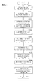
- Fig. 1 shows a flow chart of a method for manufacturing a thin film piezoelectric device according to a preferred embodiment of the present invention.
- Figs. 2A to 2E schematically show a manufacturing process of the thin film piezoelectric device formed according to the manufacturing flow shown in Fig. 1 .
- Figs. 3A to 3D schematically show a manufacturing process of the thin film piezoelectric device formed according to the manufacturing flow shown in Fig. 1 .
- Figs. 4A and 4B schematically show a manufacturing process of the thin film piezoelectric device formed according to the manufacturing flow shown in Fig. 1 .
- Fig. 5 is a graph showing the relationship between the ratio of the optical absorptance of the piezoelectric substrate 1 to that of the supporting substrate and the temperature of the bonding interface of the piezoelectric substrate and the supporting substrate when detachment is performed.
- Fig. 6 is a flow chart showing a manufacturing flow of the process of disposing a light absorbing layer.
- a manufacturing method of a piezoelectric device according to preferred embodiments of the present invention will be disclosed with reference to the accompanying drawings.
- thin film piezoelectric devices for F-BAR using a piezoelectric single crystal material will be disclosed below.
- Fig. 1 shows a flow chart of a method for manufacturing a thin film piezoelectric device according to a preferred embodiment of the present invention.
- Figs. 2A to 4B schematically show a manufacturing process of the thin film piezoelectric device formed according to the manufacturing flow shown in Fig. 1 .
- a piezoelectric single crystal substrate 1 having a specified thickness is prepared, and an ion implantation layer 100 is formed by implanting hydrogen ions from the back side surface 12 of the substrate, as sown in Fig. 2A .
- the piezoelectric substrate 1 having a number of thin film piezoelectric devices formed thereon is used.
- a hydrogen ion layer is preferably formed at a depth of about 1 ⁇ m, for example, from the back surface 12 by implanting hydrogen ions preferably with an acceleration energy of about 150 keV and at a dose amount of about 1.0 x 10 17 atom/cm 2 , for example.
- the ion implantation layer 100 is formed.
- a LT substrate a LN substrate, a Li 2 B 4 O 7 (LBO) substrate, or a La 3 Ga 5 SiO 14 (langasite) substrate, for example, may preferably be used as the piezoelectric single crystal substrate 1, and ion implantation is performed under conditions that are suitable to each of the substrates.
- LBO Li 2 B 4 O 7
- langasite La 3 Ga 5 SiO 14
- a lower electrode 20 and a lower wiring electrode 21 are formed on the back surface 12 of the piezoelectric single crystal substrate 1 preferably using aluminum (Al) or other suitable material, for example.
- an adhesive layer 30A is formed on the back surface 12 on which the lower electrode 20 and the lower wiring electrode 21 have been formed ( Fig. 1 : S102).
- a SiO 2 film is preferably used as the adhesive layer 30A, and its surface is preferably planarized by polishing, such as chemical mechanical polishing (CMP), for example.
- a supporting substrate 30B is prepared separately.
- the supporting substrate 30B is defined by forming a supporting layer 302B on a mother substrate 301B.
- an insulating material such as borosilicate glass, for example, which is a mixture of SiO 2 and B 2 O 3 and has a predetermined optical absorptance with a light having a particular wavelength is preferably used, for example.
- borosilicate glass is used for example.
- a circuit electrode pattern 50 and the supporting layer 302B preferably composed of SiO 2 , for example, are formed on the mother substrate 301B.
- a depression is formed in the area corresponding to a region at which an upper electrode described below are to be formed while a through hole is formed in the area corresponding to a portion of the circuit electrode pattern 50.
- a material for a sacrificial layer is deposited in the depression and the through hole to form sacrificial layers 40A and 40B, and the surface of the supporting layer 302B is preferably planarized by CMP, for example.
- the piezoelectric single crystal substrate 1 is attached to the supporting substrate 30B by directly bonding the supporting layer 302B of the supporting substrate 30B to the surface of the adhesive layer 30A using a surface activated bonding technology ( Fig. 1 : S103).
- the surface activated bonding is a method in which bonding is performed while a joining surface is activated by applying Ar ions or other suitable ions, for example, under a vacuum pressure. This bonding method does not require the application of heat. Even if coefficients of linear expansion between the piezoelectric single crystal substrate 1 and the adhesive layer 30A and between the adhesive layer 30A and the supporting substrate 30B are different, breakages can be prevented from occurring at each interface because the joining surface is not heated during the surface activated bonding. Furthermore, since heat is not applied to the piezoelectric single crystal substrate 1, the degradation of characteristics caused by heating is prevented. Moreover, since an OH group is not used, unlike in hydrophilic bonding, voids caused by the generation of hydrogen are also prevented.
- THG laser light 900 having wavelength 355nm is irradiated from the supporting substrate 30B side to perform detachment.
- the irradiation time is preferably set to about 100 ⁇ sec, for example.
- Optical absorptance (which is defined as 1 - (transmittance + reflectance)) with the light having a wavelength of 355nm is about 7% to about 8% for the borosilicate glass used for the supporting substrate 30B with a thickness of about 300 ⁇ m and about 35% to about 40% for a reduction treated LT substrate of the piezoelectric single crystal substrate 1 with a thickness of about 10 ⁇ m. Therefore, even if the light is irradiated from the supporting substrate 30B side, it is not significantly absorbed at the supporting substrate 30B but is primarily absorbed at the bonding surface side of the piezoelectric single crystal substrate 1.
- the temperature near the bonding interface between the piezoelectric single crystal substrate 1 and the supporting substrate 30B is locally increased.
- the ion implanted layer 100 formed near the bonding interface of the piezoelectric single crystal substrate 1 is increased to a temperature that is sufficient for heated detachment and detachment is performed.
- a piezoelectric composite substrate including a piezoelectric thin film 10 which is supported by the supporting substrate 30B is formed. Since the irradiation time of the laser light is very short, for example about 100 ⁇ sec, as described above, the temperature for detachment must be maintained for only a short amount of time. Thereby, since extended high temperature heating is not performed, degradations of piezoelectricity and insulation properties are effectively prevented. Furthermore, diffusion from the lower electrode 20 or the circuit electrode pattern 50 into the piezoelectric thin film 10 is prevented.
- Table 1 shows a relationship between the ratio of the optical absorptance of the piezoelectric substrate 1 to that of the supporting substrate 30B and the temperature of the bonding interface when detachment is performed.
- Fig. 5 is a graph illustrating the relationship shown in the Table 1.
- the temperature at the bonding interface when detachment is performed can be set to less than about 250°C.
- the temperature at the bonding interface when detachment is performed can be set to less than about 250°C, for example.
- a detached interface (surface) 13 of the piezoelectric thin film 10 is preferably polished to a mirror-smooth state by CMP or other suitable method ( Fig. 1 : S105).
- the mirror finish of the surface 13 improves the characteristics of a piezoelectric device.
- a resist film 70 is formed on the surface of the piezoelectric thin film 10 on which the upper electrode pattern has been formed and, as shown in Fig. 3B , etching windows 71 and 72 to remove the sacrificial layers 40A and 40B are formed in the resist film 70 preferably by photolithography, for example ( Fig. 1 : S107).
- the sacrificial layers 40A and 40B are removed by introducing an etching solution or an etching gas into the etching window 71.
- the space in which the sacrificial layer 40A is formed and that corresponds to the region at which the lower electrode 20 and upper electrode 60 of the single thin film piezoelectric device are formed is changed to a depletion layer 80 ( Fig. 1 : S108).
- the resist film 70 is removed as shown in Fig. 3D .
- through hole electrodes 91 that connect the circuit electrode pattern 50 to the wiring electrode 61A and the bump pad 61B are formed as an upper electrode to complete a thin film piezoelectric device while a bump 90 is formed on the bump pad 61B ( Fig. 1 : S109).
- the mother substrate is then cut into individual thin film piezoelectric devices. Thus, a thin film piezoelectric device is formed.
- the problems that arise when the known smart-cut method utilizing high temperature heating for a long period of time is used are overcome and a thin film piezoelectric device having outstanding characteristics and properties can be manufactured.
- laser light irradiation which is absorbed more easily at the piezoelectric single crystal substrate than at the supporting substrate from the supporting substrate side is described above, laser light which is absorbed more easily at the supporting substrate than at the piezoelectric single crystal substrate can preferably be irradiated from the piezoelectric single crystal substrate 1 side as well.
- a SiN film is formed thereon and polished to a mirror-smooth finish by CMP.
- laser light preferably having a wavelength of about 1.064 ⁇ m, for example, is irradiated from the piezoelectric single crystal substrate side.
- optical absorptance of the piezoelectric single crystal substrate 1 made of a LT substrate is about 20% with a thickness of about 300 ⁇ m, for example, and optical absorptance of the supporting substrate made of Si substrate is about 40% to about 50% with a thickness of about 100 ⁇ m, for example.
- the surface of the supporting substrate that is the bonding interface, is locally heated by the irradiation of the laser light from the piezoelectric single crystal substrate side, and detachment is performed. Therefore, substantially the same effects as in the manufacturing method described above are obtained with this method.
- a light absorbing layer may be disposed at the bonding interface between the piezoelectric single crystal substrate and the supporting substrate.
- Fig. 6 shows a manufacturing flow chart of a process of forming a light absorbing layer.
- the manufacturing method of a piezoelectric device including the light absorbing layer as shown in Fig, 6 differs from the manufacturing method shown in Fig. 1 in the process of forming a supporting layer including the light absorbing layer, but is the same or substantially the same in the other processes, and therefore, description of the other processes is omitted.
- a manufacturing method of a supporting substrate including a light absorbing layer includes a step of plating Ni-Zn alloy (black nickel) on a surface of a supporting substrate made of glass. Then, the surface of the plated layer is roughened by sand blasting or other suitable method, for example, and the light absorbing layer is formed. After forming a sacrificial layer on the supporting substrate in which the light absorbing layer is formed, the supporting substrate is bonded to a piezoelectric single crystal substrate ( Fig. 6 : S203). A laser light having a wavelength of about 10 ⁇ m, for example, is irradiated. The laser light is preferably irradiated in the direction from piezoelectric single crystal substrate side.
- the optical absorptance of the piezoelectric single crystal substrate including a LT substrate and the supporting substrate made of glass are about 3% to about 5% with a thickness of about 300 ⁇ m, and the optical absorptance of the light absorbing layer formed by Ni-Zn alloy is about 80% to about 90% with a thickness of 1 ⁇ m. Accordingly, laser light is absorbed near the surface of the light absorbing layer which is locally heated thereby, and detachment is performed. Therefore, substantially the same effects as the manufacturing method described above are obtained with this method.
- a light which as a broad wavelength including a plurality of these different wavelengths may preferably be used. Namely, by setting the wavelength of the laser light, the material of the piezoelectric single crystal substrate, the material of the supporting substrate, and the direction of irradiating light appropriately, effective detachment by light irradiation can be performed. Thereby, a piezoelectric device having degraded characteristics is prevented from being manufactured.
- the manufacturing method according to various preferred embodiments of the present invention can also be applied to a SAW device, a Lamb wave device, a gyro, a radio frequency (RF) switch, and other suitable devices, for example, that use a different piezoelectric thin film.
- the manufacturing method according to various preferred embodiments can further be applied to a pyroelectric device and other crystalline devices.
- a thin film piezoelectric device including a lower electrode has been described.
- the manufacturing method according to various preferred embodiments can be applied to a thin film piezoelectric device which does not include a lower electrode.
Landscapes
- Physics & Mathematics (AREA)
- Acoustics & Sound (AREA)
- Engineering & Computer Science (AREA)
- Manufacturing & Machinery (AREA)
- Piezo-Electric Or Mechanical Vibrators, Or Delay Or Filter Circuits (AREA)
- Crystals, And After-Treatments Of Crystals (AREA)
- Surface Acoustic Wave Elements And Circuit Networks Thereof (AREA)
Applications Claiming Priority (1)
| Application Number | Priority Date | Filing Date | Title |
|---|---|---|---|
| JP2009003032A JP2010161671A (ja) | 2009-01-09 | 2009-01-09 | 圧電デバイスの製造方法 |
Publications (2)
| Publication Number | Publication Date |
|---|---|
| EP2207214A2 true EP2207214A2 (de) | 2010-07-14 |
| EP2207214A3 EP2207214A3 (de) | 2011-08-03 |
Family
ID=42084537
Family Applications (1)
| Application Number | Title | Priority Date | Filing Date |
|---|---|---|---|
| EP20100150163 Withdrawn EP2207214A3 (de) | 2009-01-09 | 2010-01-06 | Verfahren zur Herstellung eines piezoelektrischen Bauteils |
Country Status (3)
| Country | Link |
|---|---|
| US (1) | US20100175236A1 (de) |
| EP (1) | EP2207214A3 (de) |
| JP (1) | JP2010161671A (de) |
Families Citing this family (2)
| Publication number | Priority date | Publication date | Assignee | Title |
|---|---|---|---|---|
| JP6947867B2 (ja) * | 2020-03-24 | 2021-10-13 | デクセリアルズ株式会社 | バルク波共振子および帯域通過フィルタ |
| CN111477543A (zh) * | 2020-04-23 | 2020-07-31 | 济南晶正电子科技有限公司 | 一种键合衬底晶圆与单晶压电晶圆的方法及复合单晶压电晶圆基板 |
Family Cites Families (9)
| Publication number | Priority date | Publication date | Assignee | Title |
|---|---|---|---|---|
| FR2788176B1 (fr) * | 1998-12-30 | 2001-05-25 | Thomson Csf | Dispositif a ondes acoustiques guidees dans une fine couche de materiau piezo-electrique collee par une colle moleculaire sur un substrat porteur et procede de fabrication |
| JP2003017967A (ja) * | 2001-06-29 | 2003-01-17 | Toshiba Corp | 弾性表面波素子及びその製造方法 |
| JP2003234455A (ja) * | 2002-02-07 | 2003-08-22 | Matsushita Electric Ind Co Ltd | 電子デバイスの製造方法、電子デバイスおよび電子デバイス装置 |
| JP2003243334A (ja) * | 2002-02-20 | 2003-08-29 | Matsushita Electric Ind Co Ltd | 電子デバイスの製造方法および電子デバイス |
| US6767749B2 (en) * | 2002-04-22 | 2004-07-27 | The United States Of America As Represented By The Secretary Of The Navy | Method for making piezoelectric resonator and surface acoustic wave device using hydrogen implant layer splitting |
| JP2008135690A (ja) * | 2006-10-30 | 2008-06-12 | Denso Corp | 半導体力学量センサおよびその製造方法 |
| KR101447048B1 (ko) * | 2007-04-20 | 2014-10-06 | 가부시키가이샤 한도오따이 에네루기 켄큐쇼 | Soi 기판 및 반도체장치의 제조방법 |
| KR101443580B1 (ko) * | 2007-05-11 | 2014-10-30 | 가부시키가이샤 한도오따이 에네루기 켄큐쇼 | Soi구조를 갖는 기판 |
| WO2008142911A1 (en) * | 2007-05-18 | 2008-11-27 | Semiconductor Energy Laboratory Co., Ltd. | Semiconductor device and method for manufacturing the same |
-
2009
- 2009-01-09 JP JP2009003032A patent/JP2010161671A/ja active Pending
-
2010
- 2010-01-06 EP EP20100150163 patent/EP2207214A3/de not_active Withdrawn
- 2010-01-07 US US12/683,521 patent/US20100175236A1/en not_active Abandoned
Also Published As
| Publication number | Publication date |
|---|---|
| JP2010161671A (ja) | 2010-07-22 |
| US20100175236A1 (en) | 2010-07-15 |
| EP2207214A3 (de) | 2011-08-03 |
Similar Documents
| Publication | Publication Date | Title |
|---|---|---|
| EP2182561B1 (de) | Verfahren zur Herstellung eines elektronischen Geräts und Verfahren zur Herstellung einer piezoelektrischen Vorrichtung | |
| US9385301B2 (en) | Method for manufacturing composite piezoelectric substrate | |
| KR101374303B1 (ko) | 압전 디바이스 및 압전 디바이스의 제조방법 | |
| EP3490144B1 (de) | Verfahren zur herstellung eines verbundsubstrats eines oberflächenwellenbauelements | |
| EP3306643B1 (de) | Verfahren zur herstellung eines verbundwafers mit einer oxid-einkristalldünnschicht | |
| US6767749B2 (en) | Method for making piezoelectric resonator and surface acoustic wave device using hydrogen implant layer splitting | |
| EP3306644B1 (de) | Verfahren zur herstellung eines verbundwafers mit oxideinkristalldünnschicht | |
| EP2624451B1 (de) | Verfahren zur herstellung einer piezoelektrischen vorrichtung | |
| KR20190014072A (ko) | 표면 음향파 디바이스용 하이브리드 구조체 | |
| WO2010143475A1 (ja) | 圧電デバイスの製造方法 | |
| EP2207214A2 (de) | Verfahren zur Herstellung eines piezoelektrischen Bauteils | |
| KR102856740B1 (ko) | 압전체 복합 기판 및 그 제조 방법 | |
| KR102870817B1 (ko) | 압전 층을 전사하는데 사용될 수 있는, 무선주파수 장치용 압전 구조체를 제조하기 위한 공정 및 이러한 압전 층을 전사하기 위한 공정 | |
| EP4102583A1 (de) | Verbundsubstrat und verfahren zur herstellung davon | |
| TW202445751A (zh) | 用於製造包含多孔矽層的多層結構的方法 | |
| KR20220158255A (ko) | 압전 층을 전사하는데 사용될 수 있는, 무선주파수 장치용 압전 구조체를 제조하기 위한 공정 및 이러한 압전 층을 전사하기 위한 공정 |
Legal Events
| Date | Code | Title | Description |
|---|---|---|---|
| PUAI | Public reference made under article 153(3) epc to a published international application that has entered the european phase |
Free format text: ORIGINAL CODE: 0009012 |
|
| AK | Designated contracting states |
Kind code of ref document: A2 Designated state(s): AT BE BG CH CY CZ DE DK EE ES FI FR GB GR HR HU IE IS IT LI LT LU LV MC MK MT NL NO PL PT RO SE SI SK SM TR |
|
| AX | Request for extension of the european patent |
Extension state: AL BA RS |
|
| PUAL | Search report despatched |
Free format text: ORIGINAL CODE: 0009013 |
|
| AK | Designated contracting states |
Kind code of ref document: A3 Designated state(s): AT BE BG CH CY CZ DE DK EE ES FI FR GB GR HR HU IE IS IT LI LT LU LV MC MK MT NL NO PL PT RO SE SI SK SM TR |
|
| AX | Request for extension of the european patent |
Extension state: AL BA RS |
|
| RIC1 | Information provided on ipc code assigned before grant |
Ipc: H03H 3/02 20060101ALI20110628BHEP Ipc: H01L 41/22 20060101AFI20110628BHEP |
|
| STAA | Information on the status of an ep patent application or granted ep patent |
Free format text: STATUS: THE APPLICATION IS DEEMED TO BE WITHDRAWN |
|
| 18D | Application deemed to be withdrawn |
Effective date: 20120204 |