EP2207837B1 - Verfahren zur herstellung einer mikroelektronischen struktur - Google Patents
Verfahren zur herstellung einer mikroelektronischen struktur Download PDFInfo
- Publication number
- EP2207837B1 EP2207837B1 EP08843358.6A EP08843358A EP2207837B1 EP 2207837 B1 EP2207837 B1 EP 2207837B1 EP 08843358 A EP08843358 A EP 08843358A EP 2207837 B1 EP2207837 B1 EP 2207837B1
- Authority
- EP
- European Patent Office
- Prior art keywords
- compound
- composition
- group
- weight
- layer
- Prior art date
- Legal status (The legal status is an assumption and is not a legal conclusion. Google has not performed a legal analysis and makes no representation as to the accuracy of the status listed.)
- Active
Links
- 0 C*CC(C)(C)C(OCC(CNC(c1cc2cc(O)ccc2cc1O)=O)O)=[U] Chemical compound C*CC(C)(C)C(OCC(CNC(c1cc2cc(O)ccc2cc1O)=O)O)=[U] 0.000 description 2
- QSAWQNUELGIYBC-UHFFFAOYSA-N OC(C(CCCC1)C1C(O)=O)=O Chemical compound OC(C(CCCC1)C1C(O)=O)=O QSAWQNUELGIYBC-UHFFFAOYSA-N 0.000 description 1
- UKONGAQTDFEZGJ-LECHCGJUSA-N OC([C@H]([C@@H](C[C@@H]1C(O)=O)C(O)=O)[C@H]1C(O)=O)O Chemical compound OC([C@H]([C@@H](C[C@@H]1C(O)=O)C(O)=O)[C@H]1C(O)=O)O UKONGAQTDFEZGJ-LECHCGJUSA-N 0.000 description 1
Images

Classifications
-
- G—PHYSICS
- G03—PHOTOGRAPHY; CINEMATOGRAPHY; ANALOGOUS TECHNIQUES USING WAVES OTHER THAN OPTICAL WAVES; ELECTROGRAPHY; HOLOGRAPHY
- G03F—PHOTOMECHANICAL PRODUCTION OF TEXTURED OR PATTERNED SURFACES, e.g. FOR PRINTING, FOR PROCESSING OF SEMICONDUCTOR DEVICES; MATERIALS THEREFOR; ORIGINALS THEREFOR; APPARATUS SPECIALLY ADAPTED THEREFOR
- G03F7/00—Photomechanical, e.g. photolithographic, production of textured or patterned surfaces, e.g. printing surfaces; Materials therefor, e.g. comprising photoresists; Apparatus specially adapted therefor
- G03F7/004—Photosensitive materials
- G03F7/09—Photosensitive materials characterised by structural details, e.g. supports, auxiliary layers
- G03F7/091—Photosensitive materials characterised by structural details, e.g. supports, auxiliary layers characterised by antireflection means or light filtering or absorbing means, e.g. anti-halation, contrast enhancement
-
- C—CHEMISTRY; METALLURGY
- C08—ORGANIC MACROMOLECULAR COMPOUNDS; THEIR PREPARATION OR CHEMICAL WORKING-UP; COMPOSITIONS BASED THEREON
- C08L—COMPOSITIONS OF MACROMOLECULAR COMPOUNDS
- C08L25/00—Compositions of, homopolymers or copolymers of compounds having one or more unsaturated aliphatic radicals, each having only one carbon-to-carbon double bond, and at least one being terminated by an aromatic carbocyclic ring; Compositions of derivatives of such polymers
- C08L25/18—Homopolymers or copolymers of aromatic monomers containing elements other than carbon and hydrogen
-
- Y—GENERAL TAGGING OF NEW TECHNOLOGICAL DEVELOPMENTS; GENERAL TAGGING OF CROSS-SECTIONAL TECHNOLOGIES SPANNING OVER SEVERAL SECTIONS OF THE IPC; TECHNICAL SUBJECTS COVERED BY FORMER USPC CROSS-REFERENCE ART COLLECTIONS [XRACs] AND DIGESTS
- Y10—TECHNICAL SUBJECTS COVERED BY FORMER USPC
- Y10S—TECHNICAL SUBJECTS COVERED BY FORMER USPC CROSS-REFERENCE ART COLLECTIONS [XRACs] AND DIGESTS
- Y10S430/00—Radiation imagery chemistry: process, composition, or product thereof
- Y10S430/151—Matting or other surface reflectivity altering material
Definitions
- the present invention is concerned with novel, photoimageable branched polymers, developer-soluble, photosensitive anti-reflective coating compositions including those polymers, and methods of using such compositions.
- a solution to this problem is to eliminate the bottom anti-reflective coating etch step by using a wet-developable or developer-soluble bottom anti-reflective coating or other wet-developable underlayers.
- Wet-developable layers typically have utilized a polyamic acid soluble in alkaline media as a polymer binder, thus allowing the film to be removed when the resist is developed.
- These traditional wet-developable materials are rendered insoluble in resist solvents by taking advantage of a thermally driven amic acid-to-imide conversion.
- the present invention is broadly concerned with a method of forming a microelectronic structure as claimed in claim 1.
- a substrate having a surface is provided, and a composition is applied to this surface.
- the composition includes a compound comprising a branched polymer, branched oligomer, or a mixture thereof, with the compound having a first molecular weight.
- the compound in the composition is crosslinked, followed by exposure of the composition to light and baking so as to decrosslink the compound and to break the compound into moieties. At least 80% of the resulting moieties have respective molecular weights that are less than the compound first molecular weight.
- the present invention solves the problem of isotropic development in prior art developer-soluble coatings by using a crosslinking/decrosslinking/depolymerization mechanism that causes the film to become alkaline-soluble only in the exposed areas. In this manner, horizontal development (undercut) is minimized or eliminated.
- the presence of small molecules after light exposure instead of macromolecules improves the imaging performance because the small molecules are more easily removed and more readily dissolved compared to macromolecules.
- compositions comprise a compound selected from the group consisting of branched polymers, branched oligomers, and mixtures thereof dissolved or dispersed in a solvent system.
- the compound i.e., the branched or non-linear polymer or oligomer
- a multi-functional acid any acidic group that can react with a vinyl ether would be suitable. More particularly, an acidic group with a pKa of 4-11 would be acceptable.
- Preferred such acidic groups include those selected from the group consisting of carboxylics, phenolics, sulfonamides, fluorinated alcohols, and mixtures thereof. Examples of suitable fluorinated alcohols include those selected from the group consisting of
- the acidic groups can be present on an oligomer, polymer, or compound.
- the acidic groups could be present on substituted and unsubstituted acrylates, methacrylates, novolaks, isocyanurates, glycidyl ethers, and mixtures thereof.
- the acid group is preferably present on the multi-functional acid oligomer or compound at a level of at least 23% by weight, more preferably from 29% to 79% by weight, and even more preferably from 39% to 78% by weight, based upon the total weight of the multi-functional acid oligomer or compound taken as 100% by weight.
- the most preferred vinyl ethers include those selected from the group consisting of ethylene glycol vinyl ether, trimethylolpropane trivinyl ether, 1,4-cyclohexane dimethanol divinyl ether, and mixtures thereof.
- Another preferred vinyl ether has a formula selected from the group consisting of , and
- the multi-functional acid and multi-functional vinyl ether are preferably reacted in the presence of an acid catalyst.
- Preferred acid catalysts are selected from the group consisting of pyridinium p -toluenesulfonate (“PPTS”), pyridinium sulfosalicylic acid, p-toluenesulfonic acid (“pTSA”), and other thermal acid generators (TAGs).
- PPTS pyridinium p -toluenesulfonate
- pTSA p-toluenesulfonic acid
- TAGs thermal acid generators
- the multi-functional acid (“MFA”) and multi-functional vinyl ether (“MFVE”) are preferably reacted at an equivalents ratio of MFA:MFVE of from 1:1.3 to 1:0.7, and more preferably from 1:1.1 to 1:0.9. Furthermore, this reaction is preferably carried out in a solvent system including solvents such as those selected from the group consisting of propylene glycol methyl ether acetate (“PGMEA”), propylene glycol methyl ether (“PGME”), propylene glycol n-propyl ether (“PnP”), ethyl lactate, propylene glycol n-butyl ether (“PnB”), cyclohexanol, tetrahydrofuran (“THF”), ether, dichloromethane, chloroform, ⁇ -butyrolactone, and mixtures thereof.
- PGMEA propylene glycol methyl ether acetate
- PnP propylene glycol methyl ether
- PnP propylene
- the solvent system has a boiling point of from 50°C to 250°C, and more preferably from 100°C to 175°C.
- the solvent system should be utilized at a level of from 65% to 99% by weight, and preferably from 69% to 98% by weight, based upon the total weight of the reaction formulation taken as 100% by weight. This reaction is preferably carried out for a time period of from 14 hours to 36 hours, preferably at ambient temperatures and preferably while stirring.
- a quencher is preferably added in order to neutralize any remaining acid, as well as any acid that might have been thermally generated during the reaction.
- the quencher would typically be added at levels of from 0.75% to 1.30% by weight, and more preferably from 0.80% to 0.85% by weight, based upon the total weight of reaction solution taken as 100% by weight.
- Suitable quenchers include those selected from the group consisting of triethanolamine ("TEA"), pyridine, and mixtures thereof.
- a number of the acid groups will react with vinyl ether groups to form an initial number of hemiacetal or acetal linkages having the formula where R is selected from the group consisting of aryls (preferably from C 6 to C 14 ), alkyls (preferably from C 1 to C 8 ), aryl alkyls (preferably from C 6 to C 12 , and from C 1 to C 8 , respectively), alkenes (preferably from C 1 to C 8 ), cyclics (preferably from C 5 to C 10 ), -CO-, -SO-, -S-, -CONH-, glycol, and adamantyl.
- R is selected from the group consisting of aryls (preferably from C 6 to C 14 ), alkyls (preferably from C 1 to C 8 ), aryl alkyls (preferably from C 6 to C 12 , and from C 1 to C 8 , respectively), alkenes (preferably from C 1 to C 8 ), cyclics (preferably from C 5 to C 10
- R groups are selected from the group consisting of , and
- Acid groups that have not reacted with the multi-functional vinyl ether are preferably present in the branched compound at a level of at least 2% by weight, preferably from 4% to 60% by weight, and even more preferably from 20% to 55% by weight, based upon the total weight of the compound taken as 100% by weight.
- vinyl groups that have not reacted with acid groups will be present at a level of at least 2% by weight, preferably from 4% to 60% by weight, and more preferably from 20% to 55% by weight, based upon the total weight of the compound taken as 100% by weight.
- the branched polymer or oligomer can be represented by the formula where:
- the unreacted acid groups are preferably not protected by a protective group. That is, at least 95%, preferably at least 98%, and more preferably 100% of the acid groups that have not reacted with the multi-functional vinyl ether are also free of protective groups.
- a protective group is a group that prevents the acid from being reactive.
- the above-described mother liquor can be used to prepare the coating composition.
- a polymer meeting the above specifications can be purchased commercially and used to make the coating formulation.
- the coating composition will be prepared by mixing additional ingredients with the mother liquor that includes the branched compound.
- One ingredient that should be included in the coating composition is a catalyst.
- the catalyst is a photoacid generator ("PAG," both ionic and/or non-ionic). Any PAG that produces an acid in the presence of light is suitable.
- Preferred PAGs include onium salts (e.g., triphenyl sulfonium perfluorosulfonates such as triphenyl sulfonium nonaflate and triphenyl sulfonium triflate), oxime-sulfonates (e.g., those sold under the name CGI ® by CIBA), and triazines (e.g., TAZ108 ® available from Midori Kagaku Company).
- onium salts e.g., triphenyl sulfonium perfluorosulfonates such as triphenyl sulfonium nonaflate and triphenyl sulfonium triflate
- oxime-sulfonates e.g., those sold under the name CGI ® by CIBA
- triazines e.g., TAZ108 ® available from Midori Kagaku Company
- the coating compositions preferably comprise from 0.35% to 10% by weight of catalyst (a PAG), and more preferably from 1% to 7% by weight of catalyst, based upon the total weight of the polymer and oligomer solids in the composition taken as 100% by weight.
- a PAG catalyst
- the coating compositions preferably comprise from 0.35% to 10% by weight of catalyst (a PAG), and more preferably from 1% to 7% by weight of catalyst, based upon the total weight of the polymer and oligomer solids in the composition taken as 100% by weight.
- the composition is essentially free of TAGs. That is, any TAGs are present at very low levels of less than 0.05% by weight, and preferably 0% by weight, based upon the total weight of the composition taken as 100% by weight.
- the inventive compositions comprise a chromophore (also referred to as a light attenuating compound or moiety or a dye).
- the chromophore can be provided as part of the branched compound (either as a functional group on the compound or as part of the polymer backbone or oligomer core), or the chromophore can simply be physically mixed in the composition.
- the chromophore should be present in the composition at a level of from 7% to 75% by weight, and preferably from 11 % to 65% by weight, based upon the total weight of the polymer and oligomer solids in the composition taken as 100% by weight.
- the chromophore is selected based upon the wavelength at which the compositions will be processed. For example, at wavelengths of 193 nm, preferred chromophores include substituted and unsubstituted phenyls (e.g., polyhydroxystyrene), heterocyclic chromophores (e.g., furan rings, thiophene rings), and functional moieties of the foregoing.
- preferred chromophores include substituted and unsubstituted phenyls (e.g., polyhydroxystyrene), heterocyclic chromophores (e.g., furan rings, thiophene rings), and functional moieties of the foregoing.
- preferred chromophores include naphthalenes (e.g., naphthoic acid methacrylate, 3,7-dihydroxy-2-naphthoic acid), heterocyclic chromophores, carbazoles, anthracenes (e.g., 9-anthracene methyl methacrylate, 9-anthracenecarboxylic acid), and functional moieties of the foregoing.
- Another preferred dye for use at 248 nm is an adduct of polyglycidyl methacrylate and 3,7-dihydroxy-2-naphthoic acid. Its formation is described in Example 2, and it has the structure where n is from 4 to 30.
- the present invention also provides a significant advantage over the prior art in that the use of an added crosslinking agent is not required, and is preferably avoided. That is, the coating composition comprises 0% by weight crosslinking agents, based upon the total weight of solids in the composition taken as 100% by weight.
- Typical optional ingredients include surfactants, amine bases, and adhesion promoters.
- the coating compositions are formed by simply dispersing or dissolving the compound (i.e., the branched polymers, branched oligomers, or mixtures thereof) in a suitable solvent system, preferably at ambient conditions and for a sufficient amount of time to form a substantially homogeneous dispersion.
- the other ingredients (PAG) are preferably dispersed or dissolved in the solvent system along with the compound.
- the branched compound could be provided as part of a mother liquor solution, with the additional ingredients being mixed with that solution, and additional solvent being added as necessary to achieve the desired solids content.
- the branched compound is preferably present in the final coating composition at a level of from 80% to 99% by weight, and more preferably from 90% to 99% by weight, based upon the total weight of the solids in the composition taken as 100% by weight.
- the preferred solids content of the final coating composition is from 0.5% to 10% by weight, more preferably from 0.5% to 6% by weight, and even more preferably from 1% to 4% by weight, based upon the total weight of the composition taken as 100% by weight.
- Preferred solvent systems include those mentioned above with respect to the mother liquor formulation.
- the solvent system has a boiling point of from 50-250 °C, and more preferably from 100-175°C.
- the solvent system should be utilized at a level of from 90% to 99.5% by weight, more preferably from 94% to 99.5% by weight, and even more preferably from 96% to 99% by weight, based upon the total weight of the composition taken as 100% by weight.
- the methods of applying the compositions to a substrate simply comprise applying a quantity of a composition hereof to the substrate surface by any known application method (including spin-coating).
- the substrate can be any conventional circuit substrate, and suitable substrates can be planar or can include topography (e.g., contact or via holes, trenches).
- Exemplary substrates include silicon, aluminum, tungsten, tungsten silicide, gallium arsenide, germanium, tantalum, tantalum nitrite, SiGe, low k dielectric layers, dielectric layers (e.g., silicon oxide), and ion implant layers.
- the resulting layer should be heated to a temperature of from 80°C to 250°C, and preferably from 140°C to 180°C, to induce crosslinking of the compound in the layer.
- Crosslinking will form further acetal bonds, with the final number of acetal bonds or linkages being greater (i.e., at least about 1.1 times, and preferably at least 1.2 times) than the initial number of acetal bonds or linkages in the branched compound prior to crosslinking.
- the crosslinked polymers or oligomers will comprise linkages having the formula where R is selected from the group consisting of aryls (preferably from C 6 to C 14 ), alkyls (preferably from C 1 to C 8 ), aryl alkyls (preferably from C 6 to C 12 , and from C 1 to C 8 , respectively), alkenes (preferably from C 1 to C 8 ), cyclics (preferably from C 5 to C 10 ), -CO-, -SO-, -S-, -CONH-, glycol, and adamantyl.
- R is selected from the group consisting of aryls (preferably from C 6 to C 14 ), alkyls (preferably from C 1 to C 8 ), aryl alkyls (preferably from C 6 to C 12 , and from C 1 to C 8 , respectively), alkenes (preferably from C 1 to C 8 ), cyclics (preferably from C 5 to C 10 ), -CO-, -SO-, -S-,
- R groups are selected from the group consisting of , and
- the crosslinked layer will be sufficiently crosslinked that it will be substantially insoluble in typical photoresist solvents.
- the inventive coating layers will have a percent stripping of less than 5%, preferably less than 1%, and even more preferably 0%.
- the stripping test involves first determining the thickness (by taking the average of measurements at five different locations) of a cured layer. This is the average initial film thickness. Next, a solvent (e.g., ethyl lactate) is puddled onto the cured film for 10 seconds, followed by spin drying at 2,000-3,500 rpm for 20-30 seconds to remove the solvent. The thickness is measured again at five different points on the wafer using ellipsometry, and the average of these measurements is determined. This is the average final film thickness.
- a solvent e.g., ethyl lactate
- the amount of stripping is the difference between the initial and final average film thicknesses.
- the crosslinked layers will also have superior light absorbance.
- the n value of this cured anti-reflective layer or coating will be at least 1.3, and preferably from 1.4 to 2.0, while the k value will be least 0.01, preferably at least 0.1, and more preferably from 0.2 to 0.8, at the wavelength of use (e.g., 157 nm, 193 nm, 248 nm, 365 nm).
- the OD of the cured layers will be at least 4/ ⁇ m, preferably from 4 to 17/ ⁇ m, and even more preferably from 9 to 15 ⁇ m, at the wavelength of use (e.g., 157 nm, 193 nm, 248nm, 365nm).
- a photoresist is applied to the cured layer and subsequently patterned by exposure to light of the appropriate wavelength followed by a post-exposure bake (preferably from 70°C to 150°C, more preferably from 90°C to 130 °C) and development of the exposed photoresist.
- the photoresist is exposed to light, so is the inventive coating.
- an acid is generated from the PAG, and this acid "decrosslinks" the compound in the layer. Furthermore, the acid "depolymerizes" the compound as well.
- the acid catalyzes the breaking of at least one of (and preferably of both) the C-O bonds (designated by "*" below) of the hemiacetal ester or acetal that was present in the branched compound as well as those that were created during thermal crosslinking.
- R 1 and R 2 can be the same or different, and include the same variables as described previously for R.
- Some of these developers are commercialized under the names PD523AD (available from JSR Micro), MF-319 (available from Rohm & Haas, Massachusetts), and NMD3 (available from TOK, Japan) developers. At least 95%, preferably at least about 99%, and even more preferably 100% of the inventive coatings will be removed within 120 seconds by a base developer such as tetramethyl ammonium hydroxide and/or KOH developers after light exposure. This high percent solubility in commercially-available developers after light exposure is a significant advantage over the prior art as this shortens the manufacturing process and makes it less costly.
- trimesic acid obtained from Fluka, Milwaukee, WI
- PGME propylene glycol monomethyl ether
- 420 mg of a trifunctional vinyl ether were added to the solution, together with 5 mg of PPTS (obtained from Aldrich, Milwaukee, WI).
- the reaction mixture was stirred overnight at room temperature, and then 20 mg of TEA (obtained from Aldrich, Milwaukee, WI) were added to neutralize any remaining acid content (and acid thermally generated during baking).
- Triphenylsulfonium triflate (“TPS-Tf,” obtained from Aldrich, Milwaukee, WI) was added as a PAG at a level of 5% by weight, based upon the total weight of the composition taken as 100% by weight.
- the reaction mixture was diluted by PGME to a solids level of 2.5% and filtered through a 0.1-micron endpoint filter.
- the formulation was spin-coated at 2,000 rpm onto a silicon substrate and then baked at 150°C for 60 seconds.
- the optical constants were measured using a variable angle spectroscopic ellipsometer ("VASE,” from J.A. Woollam Co., Inc.) and were determined to be: n at 193 nm was 1.379; and k at 193 nm was 0.374.
- VASE variable angle spectroscopic ellipsometer
- glycidyl methacrylate obtained from Harcros, St. Louis, MO
- cyclohexanone obtained from Harcros, St. Louis, MO
- the mixture was stirred at room temperature for 5 minutes, until a homogeneous solution was produced.
- a dropping funnel and condenser were attached to the flask, and the whole setup was protected under nitrogen flow.
- the dropping funnel was filled with a solution containing 69.3 g of cyclohexanone (obtained from Harcros, St.
- the PGM/3,7-DNA polymeric dye was obtained by precipitating into 35/65 by weight PGME/deionized water, re-dissolving in PGME, re-precipitating into hexanes, and vacuum-drying at 50°C.
- a branched polymer scaffold was first synthesized following the method described in Example 1.
- 246 mg of cyclopentane tetracarboxylic acid obtained from Aldrich, Milwaukee, WI
- PGME polyhydroxyethyl ether
- 560 mg of the trifunctional vinyl ether described in Example 1 were added into the solution, together with 5 mg of PPTS.
- the reaction mixture was stirred overnight at room temperature, and then 20 mg of TEA were added.
- Branched polyhydroxystyrene (obtained from Hydrite Chemical Company, Brookfield, WI) was selected as a 193-nm dye to add to the above reaction mixture.
- the dye was utilized at a level of 30% by weight, based upon the total solids of the reaction mixture.
- the resultant solution was further diluted with PGME to total solids content of 2.5% by weight, and TPS-Tf was added as a PAG at a level of 5% by weight, based upon the total solids in the formulation taken as 100% by weight.
- the formulation was spin-coated at 2,000 rpm onto a silicon substrate and then baked at 150°C for 60 seconds.
- the PGM/3,7-DNA prepared in Example 2 was used as a 248-nm dye to be added into the original branched polymer solution.
- the dye level varied from 0% to 60% by weight of the total solids content of the formulation, which gave various optical constants.
- TPS-Tf was added as a PAG at a level of 5% by weight of the total solids content of the formulation.
- the resultant solution was further diluted by PGME to a total solids content of 2.5% by weight.
- the formulation was spin-coated at 1,500 rpm onto a silicon substrate and then baked at 150°C for 60 seconds, followed by EL stripping and dark loss testing. All results are summarized in Table 3.
- TPS-Tf in the amount of 100 mg, was added to the formulation as a PAG.
- the reaction mixture was diluted by adding PGME to achieve a total solids content of 2.5% by weight, followed by filtering through 0.1-micron endpoint filter.
- the formulation was spin-coated at 1,500 rpm onto a silicon substrate and then baked at 150°C for 60 seconds.
- the optical constants were measured using a VASE and were determined to be: n at 193 nm was 1.430; k at 193 nm was 0.246, n at 248 nm was 1.752, and k at 248 nm was 0.275.
- TPS-Tf was added as a PAG at a level of 5% by weight of the total solids weight.
- the reaction mixture was diluted by PGME to 2.5% and filtered through 0.1-micron endpoint filter.
- the formulation was spin-coated at 1,500 rpm onto a silicon substrate and then baked at 160°C for 60 seconds.
- the optical constants were measured using a VASE and were determined to be: n at 193 nm was 1.704; k at 193 nm was 0.015; n at 248 was 1.587; and k at 248 was 0.003.
- Results from EL stripping, dark loss, and exposure/PEB/development testing are summarized in Table 5.
- Table 5 Film Properties of Example 5 30-second EL Strip Exposure, PEB, and Development Development Without Exposure
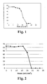
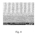
- a film made with the coating formulation of this Example was imaged by exposure to a mercury-xenon lamp with a 248-nm filter under a photomask (contact mode), followed by PEB at 130°C for 60 seconds and rinsing with tetramethylammonium hydroxide (TMAH) developer.
- TMAH tetramethylammonium hydroxide
- the minimum exposure dose required was less than 20 mJ/cm 2 .
- Fig. 3 shows a micrograph of the patterned film.
- TPS-Tf was added as a PAG at a level of 5% by weight of the total solids content of the formulation.
- the reaction mixture was diluted by PGME to 2.5% and was filtered through 0.1-micron endpoint filter.
- the formulation was spin-coated at 2,000 rpm onto a silicon substrate and then baked at 150°C for 60 seconds.
- the optical constants were measured using a VASE and were determined to be: n at 193 nm was 1.447; k at 193 nm was 0.246; n at 248 nm was 1.731; and k at 248 nm was 0.024.
- Results from EL stripping, dark loss, and exposure/PEB/development testing are summarized in Table 6. Table 6. Film Properties of Example 6 30-second EL Strip Exposure, PEB, and Development Development Without Exposure Initial Thickness ( ⁇ ) 520 555 524 Thickness after Treatment ( ⁇ ) 502 0 520 % change -3.4% -100% -0.7%
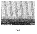
- the wafer was then exposed through an in-house interferometer lithographic tool, targeting at 120-nm, dense line patterning. After a PEB at 130°C for 60 seconds and development using PD523AD, the wafer was cross-section for SEM imaging (see Fig. 4 ). The bottom anti-reflective coating layer was cleared together with the top photoresist, without obvious footing or undercutting.
- trimesic acid from Aldrich
- PGME polymethyl methacrylate
- 672 mg of the trifunctional vinyl ether described in Example 1 were added into the solution, together with 10 mg of PPTS.
- the reaction mixture was stirred overnight at room temperature.
- 5.6 mg of TEA were added as quencher
- 30.0 mg TPS-triflate were added as PAG, and the mixture was diluted by PGME to 2.5% and filtered through 0.1-micron endpoint filter.
- the formulation was spin-coated at 1,500 rpm onto a silicon substrate and then baked at 160°C for 60 seconds.
- ARX 3001 resist obtained from JSR Micro
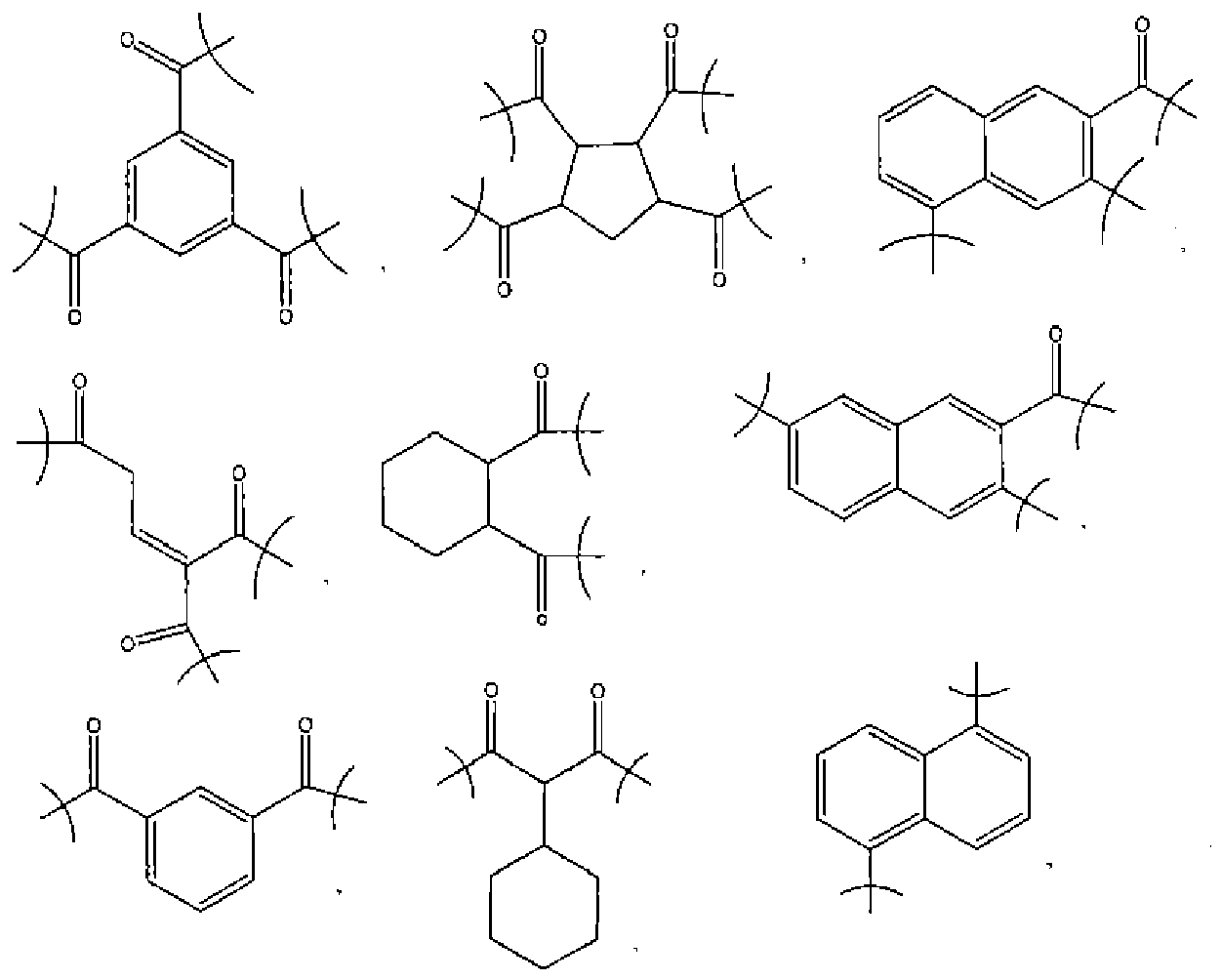
- the wafer was then exposed through an in-house interferometer lithographic tool, targeting at 150-nm, dense line patterning.
- PEB at 110°C for 60 seconds and development using PD523AD
- the wafer was cross-section for SEM imaging (see Fig. 5 ).
- the bottom anti-reflective layer was cleared together with the top photoresist, without obvious footing or undercutting.
Landscapes
- Engineering & Computer Science (AREA)
- Architecture (AREA)
- Structural Engineering (AREA)
- Physics & Mathematics (AREA)
- General Physics & Mathematics (AREA)
- Materials For Photolithography (AREA)
- Addition Polymer Or Copolymer, Post-Treatments, Or Chemical Modifications (AREA)
- Other Resins Obtained By Reactions Not Involving Carbon-To-Carbon Unsaturated Bonds (AREA)
- Exposure Of Semiconductors, Excluding Electron Or Ion Beam Exposure (AREA)
Claims (12)
- Verfahren zur Bildung einer mikroelektronischen Struktur, wobei das Verfahren umfasst:Bereitstellung eines Substrats mit einer Oberfläche; Aufbringung einer photosensitiven Antireflex-Beschichtungszusammensetzung, wobei die Zusammensetzung einen Photosäuregenerator und eine Verbindung enthält, die ein verzweigtes Polymer, verzweigtes Oligomer oder eine Mischung derselben umfasst, wobei die Verbindung ein erstes Molekulargewicht aufweist und eine mit einem Vinylether umgesetzte Säuregruppe umfasst, wie sie durch umsetzung einer multifunktionalen Säure mit einem multifunktionalen Vinylether gebildet wird, wobei die Verbindung eine Anfangszahl von Bindungen mit der Formel
 thermische Vernetzung der Verbindung in der Zusammensetzung, um eine vernetzte Schicht zu erhalten;Aufbringung einer Photoresist-Schicht auf diese Schicht;Aussetzen Photoresist-Schicht und der vernetzten Schicht gegenüber Licht gefolgt von einem Schritt des Backens, um so die Verbindung zu entnetzen und die Verbindung in kleine Moleküle zu zerbrechen, wobei mindestens 80% dieser kleinen Moleküle jeweils Molekulargewichte aufwiesen, die kleiner sind als das erste Molekulargewicht; undIn-Kontakt-Bringen der kleinen Moleküle mit einem Entwickler, um so die kleinen Moleküle von der Oberfläche zu entfernen.
 - Verfahren nach Anspruch 1, bei dem die Säuregruppe aus der Gruppe bestehend aus Carboxylen, Phenolen, Sulfonamiden, fluorierten Alkoholen und Mischungen derselben ausgewählt ist.
- Verfahren nach Anspruch 1, bei dem R aus der Gruppe bestehend aus
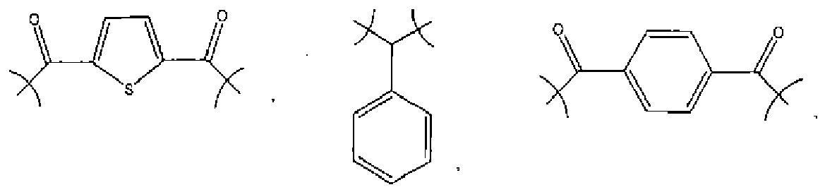


- Verfahren nach Anspruch 1, bei dem die Vernetzung eine Schicht der Zusammensetzung ergibt, die im Wesentlichen in Photoresist-Lösungsmitteln unlöslich ist.
- Verfahren nach Anspruch 1, bei dem die Vernetzung zu vernetzten Verbindungen führt, die eine Endzahl an Bindungen mit der Formel

- Verfahren nach Anspruch 1, bei dem das Aussetzen und das Backen eine Schicht ergeben, die im Wesentlichen in Photoresist-Lösungsmitteln löslich ist.
- Verfahren nach Anspruch 1, bei dem das Aussetzen und das Backen zum Brechen von mindestens einer der Bindungen (*) der Bindung mit der Formel führt,

- Verfahren nach Anspruch 1, bei dem das Substrat ein mikroelektronisches Substrat ist.
- Verfahren nach Anspruch 9, bei dem das Substrat aus der Gruppe bestehend aus Silicium, Aluminium, Wolfram, Wolframsilicid, Galliumarsenid, Germanium, Tantal, Tantalnitrite, SiGe, Ionenimplantatschichten, dielektrischen Schichten mit niedrigem k-Wert und dielektrischen Schicht ausgewählt ist.
- Verfahren nach Anspruch 9, bei dem
das Substrat ferner ein strukturdefinierendes Loch aufweist, wobei die Struktur Seitenwände und eine Bodenwand aufweist; und
die Aufbringung die Aufbringung der Zusammensetzung auf mindestens einen Teil der Lochseitenwände und der Bodenwand umfasst. - Verfahren nach Anspruch 9, bei dem das Substrat eine Ionenimplantatschicht umfasst und die Aufbringung das Bilden einer Schicht der Zusammensetzung angrenzend an die Ionenimplantatschicht umfasst.
- Verfahren nach Anspruch 1, bei dem die Verbindung ferner nicht-umgesetzte Säuregruppen umfasst, wobei mindestens 95% der nicht-umgesetzten Säuregruppen frei von Schutzgruppen sind.
Applications Claiming Priority (2)
| Application Number | Priority Date | Filing Date | Title |
|---|---|---|---|
| US98377807P | 2007-10-30 | 2007-10-30 | |
| PCT/US2008/081831 WO2009059031A2 (en) | 2007-10-30 | 2008-10-30 | Photoimageable branched polymer |
Publications (3)
| Publication Number | Publication Date |
|---|---|
| EP2207837A2 EP2207837A2 (de) | 2010-07-21 |
| EP2207837A4 EP2207837A4 (de) | 2010-12-01 |
| EP2207837B1 true EP2207837B1 (de) | 2015-03-25 |
Family
ID=40583287
Family Applications (1)
| Application Number | Title | Priority Date | Filing Date |
|---|---|---|---|
| EP08843358.6A Active EP2207837B1 (de) | 2007-10-30 | 2008-10-30 | Verfahren zur herstellung einer mikroelektronischen struktur |
Country Status (6)
| Country | Link |
|---|---|
| US (1) | US8206893B2 (de) |
| EP (1) | EP2207837B1 (de) |
| JP (1) | JP2011502286A (de) |
| KR (1) | KR101211325B1 (de) |
| CN (1) | CN101842414B (de) |
| WO (1) | WO2009059031A2 (de) |
Families Citing this family (8)
| Publication number | Priority date | Publication date | Assignee | Title |
|---|---|---|---|---|
| JPWO2009038126A1 (ja) * | 2007-09-20 | 2011-01-06 | 日産化学工業株式会社 | 分岐型ポリヒドロキシスチレンを含むレジスト下層膜形成組成物 |
| US8883407B2 (en) * | 2009-06-12 | 2014-11-11 | Rohm And Haas Electronic Materials Llc | Coating compositions suitable for use with an overcoated photoresist |
| US8877430B2 (en) | 2010-08-05 | 2014-11-04 | Brewer Science Inc. | Methods of producing structures using a developer-soluble layer with multilayer technology |
| JP6230217B2 (ja) * | 2011-09-06 | 2017-11-15 | Jsr株式会社 | レジストパターン形成方法 |
| US10331032B2 (en) | 2012-04-23 | 2019-06-25 | Brewer Science, Inc. | Photosensitive, developer-soluble bottom anti-reflective coating material |
| JP6117711B2 (ja) * | 2014-02-06 | 2017-04-19 | 信越化学工業株式会社 | 半導体基板の洗浄乾燥方法 |
| US10388510B2 (en) | 2018-01-12 | 2019-08-20 | International Business Machines Corporation | Wet strippable OPL using reversible UV crosslinking and de-crosslinking |
| KR102285555B1 (ko) * | 2018-06-12 | 2021-08-03 | 주식회사 엘지화학 | 코팅 조성물 및 이를 이용한 마이크로 전자 소자 제조용 포지티브형 패턴의 제조방법 |
Family Cites Families (18)
| Publication number | Priority date | Publication date | Assignee | Title |
|---|---|---|---|---|
| US6054254A (en) | 1997-07-03 | 2000-04-25 | Kabushiki Kaisha Toshiba | Composition for underlying film and method of forming a pattern using the film |
| JP3852889B2 (ja) * | 1998-09-24 | 2006-12-06 | 富士写真フイルム株式会社 | フォトレジスト用反射防止膜材料組成物 |
| JP4031593B2 (ja) * | 1999-04-13 | 2008-01-09 | 太陽インキ製造株式会社 | ポジ型感光性樹脂組成物 |
| US6110653A (en) | 1999-07-26 | 2000-08-29 | International Business Machines Corporation | Acid sensitive ARC and method of use |
| JP4166417B2 (ja) * | 1999-11-29 | 2008-10-15 | 富士フイルム株式会社 | ポジ型レジスト積層物 |
| US6844131B2 (en) | 2002-01-09 | 2005-01-18 | Clariant Finance (Bvi) Limited | Positive-working photoimageable bottom antireflective coating |
| US7070914B2 (en) | 2002-01-09 | 2006-07-04 | Az Electronic Materials Usa Corp. | Process for producing an image using a first minimum bottom antireflective coating composition |
| US7261997B2 (en) | 2002-01-17 | 2007-08-28 | Brewer Science Inc. | Spin bowl compatible polyamic acids/imides as wet developable polymer binders for anti-reflective coatings |
| KR20040009384A (ko) | 2002-07-23 | 2004-01-31 | 삼성전자주식회사 | 포토레지스트용 현상액에 용해되는 유기 바닥 반사 방지조성물과 이를 이용한 사진 식각 공정 |
| KR100813458B1 (ko) * | 2003-05-20 | 2008-03-13 | 도오꾜오까고오교 가부시끼가이샤 | 화학증폭형 포지티브형 포토레지스트 조성물 및 레지스트패턴형성방법 |
| TWI363251B (en) * | 2003-07-30 | 2012-05-01 | Nissan Chemical Ind Ltd | Sublayer coating-forming composition for lithography containing compound having protected carboxy group |
| US20050214674A1 (en) * | 2004-03-25 | 2005-09-29 | Yu Sui | Positive-working photoimageable bottom antireflective coating |
| US20050255410A1 (en) * | 2004-04-29 | 2005-11-17 | Guerrero Douglas J | Anti-reflective coatings using vinyl ether crosslinkers |
| US7816071B2 (en) | 2005-02-10 | 2010-10-19 | Az Electronic Materials Usa Corp. | Process of imaging a photoresist with multiple antireflective coatings |
| US20060177772A1 (en) | 2005-02-10 | 2006-08-10 | Abdallah David J | Process of imaging a photoresist with multiple antireflective coatings |
| WO2007086249A1 (ja) * | 2006-01-25 | 2007-08-02 | Nissan Chemical Industries, Ltd. | ポジ型感光性樹脂組成物及びそれから得られる硬化膜 |
| EP1845416A3 (de) * | 2006-04-11 | 2009-05-20 | Rohm and Haas Electronic Materials, L.L.C. | Beschichtungszusammensetzungen für Photolithographie |
| US7816069B2 (en) | 2006-06-23 | 2010-10-19 | International Business Machines Corporation | Graded spin-on organic antireflective coating for photolithography |
-
2008
- 2008-10-30 JP JP2010532250A patent/JP2011502286A/ja active Pending
- 2008-10-30 WO PCT/US2008/081831 patent/WO2009059031A2/en not_active Ceased
- 2008-10-30 KR KR1020107010221A patent/KR101211325B1/ko active Active
- 2008-10-30 US US12/261,971 patent/US8206893B2/en active Active
- 2008-10-30 EP EP08843358.6A patent/EP2207837B1/de active Active
- 2008-10-30 CN CN200880114522.7A patent/CN101842414B/zh active Active
Also Published As
| Publication number | Publication date |
|---|---|
| US8206893B2 (en) | 2012-06-26 |
| KR101211325B1 (ko) | 2012-12-12 |
| KR20100087157A (ko) | 2010-08-03 |
| EP2207837A2 (de) | 2010-07-21 |
| US20090111057A1 (en) | 2009-04-30 |
| CN101842414B (zh) | 2014-06-04 |
| JP2011502286A (ja) | 2011-01-20 |
| WO2009059031A3 (en) | 2009-08-06 |
| EP2207837A4 (de) | 2010-12-01 |
| WO2009059031A2 (en) | 2009-05-07 |
| CN101842414A (zh) | 2010-09-22 |
Similar Documents
| Publication | Publication Date | Title |
|---|---|---|
| EP1743219B1 (de) | Verfahren zur herstellung von mikroelektronischen strukturen, die antireflexbeschichtungen enthalten, unter anwendung von vinylether-vernetzern | |
| EP2207837B1 (de) | Verfahren zur herstellung einer mikroelektronischen struktur | |
| EP2089770B1 (de) | Verfahren zur erzeugung von fotolithografischen strukturen mit entwicklergetrimmter hartmaske | |
| TWI558778B (zh) | 底部抗反射塗料組合物及其方法 | |
| EP2399169B1 (de) | Säureempfindliche entwicklerlösliche antireflexgrundbeschichtungen | |
| KR101820263B1 (ko) | 반사방지 코팅 조성물 및 이의 공정 | |
| EP1470446B1 (de) | Organische antireflexbeschichtungszusammensetzungen für die fortgeschrittene mikrolithographie | |
| US20070207406A1 (en) | Anti-reflective coatings using vinyl ether crosslinkers | |
| EP1573785B1 (de) | Boden-antireflexbeschichtungen auf basis kleiner moleküle mit multiplen epoxy-einheiten | |
| TWI491995B (zh) | 用於光阻之抗反射組合物 | |
| WO2008150058A1 (en) | Hardmask composition having antireflective properties and method of patterning material on substrate using the same | |
| KR101561051B1 (ko) | 포토리소그래피용 코팅 조성물 | |
| JP2021005116A (ja) | モノマー、ポリマーおよびこれを含むリソグラフィ組成物 | |
| WO2007032574A1 (en) | Antireflective hardmask composition and methods for using same | |
| TWI436165B (zh) | 可光成像分枝聚合物 |
Legal Events
| Date | Code | Title | Description |
|---|---|---|---|
| PUAI | Public reference made under article 153(3) epc to a published international application that has entered the european phase |
Free format text: ORIGINAL CODE: 0009012 |
|
| 17P | Request for examination filed |
Effective date: 20100426 |
|
| AK | Designated contracting states |
Kind code of ref document: A2 Designated state(s): AT BE BG CH CY CZ DE DK EE ES FI FR GB GR HR HU IE IS IT LI LT LU LV MC MT NL NO PL PT RO SE SI SK TR |
|
| AX | Request for extension of the european patent |
Extension state: AL BA MK RS |
|
| A4 | Supplementary search report drawn up and despatched |
Effective date: 20101103 |
|
| 17Q | First examination report despatched |
Effective date: 20120514 |
|
| DAX | Request for extension of the european patent (deleted) | ||
| GRAP | Despatch of communication of intention to grant a patent |
Free format text: ORIGINAL CODE: EPIDOSNIGR1 |
|
| INTG | Intention to grant announced |
Effective date: 20141105 |
|
| GRAS | Grant fee paid |
Free format text: ORIGINAL CODE: EPIDOSNIGR3 |
|
| GRAA | (expected) grant |
Free format text: ORIGINAL CODE: 0009210 |
|
| AK | Designated contracting states |
Kind code of ref document: B1 Designated state(s): AT BE BG CH CY CZ DE DK EE ES FI FR GB GR HR HU IE IS IT LI LT LU LV MC MT NL NO PL PT RO SE SI SK TR |
|
| REG | Reference to a national code |
Ref country code: GB Ref legal event code: FG4D |
|
| REG | Reference to a national code |
Ref country code: CH Ref legal event code: EP |
|
| REG | Reference to a national code |
Ref country code: IE Ref legal event code: FG4D |
|
| REG | Reference to a national code |
Ref country code: DE Ref legal event code: R096 Ref document number: 602008037359 Country of ref document: DE Effective date: 20150507 |
|
| REG | Reference to a national code |
Ref country code: AT Ref legal event code: REF Ref document number: 717853 Country of ref document: AT Kind code of ref document: T Effective date: 20150515 |
|
| PG25 | Lapsed in a contracting state [announced via postgrant information from national office to epo] |
Ref country code: LT Free format text: LAPSE BECAUSE OF FAILURE TO SUBMIT A TRANSLATION OF THE DESCRIPTION OR TO PAY THE FEE WITHIN THE PRESCRIBED TIME-LIMIT Effective date: 20150325 Ref country code: SE Free format text: LAPSE BECAUSE OF FAILURE TO SUBMIT A TRANSLATION OF THE DESCRIPTION OR TO PAY THE FEE WITHIN THE PRESCRIBED TIME-LIMIT Effective date: 20150325 Ref country code: HR Free format text: LAPSE BECAUSE OF FAILURE TO SUBMIT A TRANSLATION OF THE DESCRIPTION OR TO PAY THE FEE WITHIN THE PRESCRIBED TIME-LIMIT Effective date: 20150325 Ref country code: FI Free format text: LAPSE BECAUSE OF FAILURE TO SUBMIT A TRANSLATION OF THE DESCRIPTION OR TO PAY THE FEE WITHIN THE PRESCRIBED TIME-LIMIT Effective date: 20150325 |
|
| REG | Reference to a national code |
Ref country code: AT Ref legal event code: MK05 Ref document number: 717853 Country of ref document: AT Kind code of ref document: T Effective date: 20150325 |
|
| REG | Reference to a national code |
Ref country code: LT Ref legal event code: MG4D |
|
| PG25 | Lapsed in a contracting state [announced via postgrant information from national office to epo] |
Ref country code: GR Free format text: LAPSE BECAUSE OF FAILURE TO SUBMIT A TRANSLATION OF THE DESCRIPTION OR TO PAY THE FEE WITHIN THE PRESCRIBED TIME-LIMIT Effective date: 20150626 Ref country code: LV Free format text: LAPSE BECAUSE OF FAILURE TO SUBMIT A TRANSLATION OF THE DESCRIPTION OR TO PAY THE FEE WITHIN THE PRESCRIBED TIME-LIMIT Effective date: 20150325 |
|
| PG25 | Lapsed in a contracting state [announced via postgrant information from national office to epo] |
Ref country code: NL Free format text: LAPSE BECAUSE OF FAILURE TO SUBMIT A TRANSLATION OF THE DESCRIPTION OR TO PAY THE FEE WITHIN THE PRESCRIBED TIME-LIMIT Effective date: 20150325 |
|
| PG25 | Lapsed in a contracting state [announced via postgrant information from national office to epo] |
Ref country code: PT Free format text: LAPSE BECAUSE OF FAILURE TO SUBMIT A TRANSLATION OF THE DESCRIPTION OR TO PAY THE FEE WITHIN THE PRESCRIBED TIME-LIMIT Effective date: 20150727 Ref country code: ES Free format text: LAPSE BECAUSE OF FAILURE TO SUBMIT A TRANSLATION OF THE DESCRIPTION OR TO PAY THE FEE WITHIN THE PRESCRIBED TIME-LIMIT Effective date: 20150325 Ref country code: SK Free format text: LAPSE BECAUSE OF FAILURE TO SUBMIT A TRANSLATION OF THE DESCRIPTION OR TO PAY THE FEE WITHIN THE PRESCRIBED TIME-LIMIT Effective date: 20150325 Ref country code: RO Free format text: LAPSE BECAUSE OF FAILURE TO SUBMIT A TRANSLATION OF THE DESCRIPTION OR TO PAY THE FEE WITHIN THE PRESCRIBED TIME-LIMIT Effective date: 20150325 Ref country code: EE Free format text: LAPSE BECAUSE OF FAILURE TO SUBMIT A TRANSLATION OF THE DESCRIPTION OR TO PAY THE FEE WITHIN THE PRESCRIBED TIME-LIMIT Effective date: 20150325 Ref country code: CZ Free format text: LAPSE BECAUSE OF FAILURE TO SUBMIT A TRANSLATION OF THE DESCRIPTION OR TO PAY THE FEE WITHIN THE PRESCRIBED TIME-LIMIT Effective date: 20150325 |
|
| PG25 | Lapsed in a contracting state [announced via postgrant information from national office to epo] |
Ref country code: PL Free format text: LAPSE BECAUSE OF FAILURE TO SUBMIT A TRANSLATION OF THE DESCRIPTION OR TO PAY THE FEE WITHIN THE PRESCRIBED TIME-LIMIT Effective date: 20150325 Ref country code: AT Free format text: LAPSE BECAUSE OF FAILURE TO SUBMIT A TRANSLATION OF THE DESCRIPTION OR TO PAY THE FEE WITHIN THE PRESCRIBED TIME-LIMIT Effective date: 20150325 Ref country code: IS Free format text: LAPSE BECAUSE OF FAILURE TO SUBMIT A TRANSLATION OF THE DESCRIPTION OR TO PAY THE FEE WITHIN THE PRESCRIBED TIME-LIMIT Effective date: 20150725 |
|
| REG | Reference to a national code |
Ref country code: DE Ref legal event code: R097 Ref document number: 602008037359 Country of ref document: DE |
|
| PG25 | Lapsed in a contracting state [announced via postgrant information from national office to epo] |
Ref country code: DK Free format text: LAPSE BECAUSE OF FAILURE TO SUBMIT A TRANSLATION OF THE DESCRIPTION OR TO PAY THE FEE WITHIN THE PRESCRIBED TIME-LIMIT Effective date: 20150325 |
|
| PLBE | No opposition filed within time limit |
Free format text: ORIGINAL CODE: 0009261 |
|
| STAA | Information on the status of an ep patent application or granted ep patent |
Free format text: STATUS: NO OPPOSITION FILED WITHIN TIME LIMIT |
|
| 26N | No opposition filed |
Effective date: 20160105 |
|
| PG25 | Lapsed in a contracting state [announced via postgrant information from national office to epo] |
Ref country code: IT Free format text: LAPSE BECAUSE OF FAILURE TO SUBMIT A TRANSLATION OF THE DESCRIPTION OR TO PAY THE FEE WITHIN THE PRESCRIBED TIME-LIMIT Effective date: 20150325 |
|
| PG25 | Lapsed in a contracting state [announced via postgrant information from national office to epo] |
Ref country code: SI Free format text: LAPSE BECAUSE OF FAILURE TO SUBMIT A TRANSLATION OF THE DESCRIPTION OR TO PAY THE FEE WITHIN THE PRESCRIBED TIME-LIMIT Effective date: 20150325 Ref country code: LU Free format text: LAPSE BECAUSE OF FAILURE TO SUBMIT A TRANSLATION OF THE DESCRIPTION OR TO PAY THE FEE WITHIN THE PRESCRIBED TIME-LIMIT Effective date: 20151030 |
|
| REG | Reference to a national code |
Ref country code: CH Ref legal event code: PL |
|
| GBPC | Gb: european patent ceased through non-payment of renewal fee |
Effective date: 20151030 |
|
| PG25 | Lapsed in a contracting state [announced via postgrant information from national office to epo] |
Ref country code: MC Free format text: LAPSE BECAUSE OF FAILURE TO SUBMIT A TRANSLATION OF THE DESCRIPTION OR TO PAY THE FEE WITHIN THE PRESCRIBED TIME-LIMIT Effective date: 20150325 |
|
| REG | Reference to a national code |
Ref country code: IE Ref legal event code: MM4A |
|
| PG25 | Lapsed in a contracting state [announced via postgrant information from national office to epo] |
Ref country code: CH Free format text: LAPSE BECAUSE OF NON-PAYMENT OF DUE FEES Effective date: 20151031 Ref country code: LI Free format text: LAPSE BECAUSE OF NON-PAYMENT OF DUE FEES Effective date: 20151031 Ref country code: GB Free format text: LAPSE BECAUSE OF NON-PAYMENT OF DUE FEES Effective date: 20151030 |
|
| PG25 | Lapsed in a contracting state [announced via postgrant information from national office to epo] |
Ref country code: BE Free format text: LAPSE BECAUSE OF FAILURE TO SUBMIT A TRANSLATION OF THE DESCRIPTION OR TO PAY THE FEE WITHIN THE PRESCRIBED TIME-LIMIT Effective date: 20150325 |
|
| REG | Reference to a national code |
Ref country code: FR Ref legal event code: PLFP Year of fee payment: 9 |
|
| PG25 | Lapsed in a contracting state [announced via postgrant information from national office to epo] |
Ref country code: IE Free format text: LAPSE BECAUSE OF NON-PAYMENT OF DUE FEES Effective date: 20151030 |
|
| PG25 | Lapsed in a contracting state [announced via postgrant information from national office to epo] |
Ref country code: HU Free format text: LAPSE BECAUSE OF FAILURE TO SUBMIT A TRANSLATION OF THE DESCRIPTION OR TO PAY THE FEE WITHIN THE PRESCRIBED TIME-LIMIT; INVALID AB INITIO Effective date: 20081030 Ref country code: NO Free format text: LAPSE BECAUSE OF FAILURE TO SUBMIT A TRANSLATION OF THE DESCRIPTION OR TO PAY THE FEE WITHIN THE PRESCRIBED TIME-LIMIT Effective date: 20150625 Ref country code: BG Free format text: LAPSE BECAUSE OF FAILURE TO SUBMIT A TRANSLATION OF THE DESCRIPTION OR TO PAY THE FEE WITHIN THE PRESCRIBED TIME-LIMIT Effective date: 20150325 |
|
| PG25 | Lapsed in a contracting state [announced via postgrant information from national office to epo] |
Ref country code: CY Free format text: LAPSE BECAUSE OF FAILURE TO SUBMIT A TRANSLATION OF THE DESCRIPTION OR TO PAY THE FEE WITHIN THE PRESCRIBED TIME-LIMIT Effective date: 20150325 |
|
| PG25 | Lapsed in a contracting state [announced via postgrant information from national office to epo] |
Ref country code: MT Free format text: LAPSE BECAUSE OF FAILURE TO SUBMIT A TRANSLATION OF THE DESCRIPTION OR TO PAY THE FEE WITHIN THE PRESCRIBED TIME-LIMIT Effective date: 20150325 Ref country code: TR Free format text: LAPSE BECAUSE OF FAILURE TO SUBMIT A TRANSLATION OF THE DESCRIPTION OR TO PAY THE FEE WITHIN THE PRESCRIBED TIME-LIMIT Effective date: 20150325 |
|
| REG | Reference to a national code |
Ref country code: FR Ref legal event code: PLFP Year of fee payment: 10 |
|
| REG | Reference to a national code |
Ref country code: FR Ref legal event code: PLFP Year of fee payment: 11 |
|
| PGFP | Annual fee paid to national office [announced via postgrant information from national office to epo] |
Ref country code: DE Payment date: 20241029 Year of fee payment: 17 |
|
| PGFP | Annual fee paid to national office [announced via postgrant information from national office to epo] |
Ref country code: FR Payment date: 20241025 Year of fee payment: 17 |