EP2208400B1 - Alimentation en courant commutable pour circuits auxiliaires dans un convertisseur - Google Patents
Alimentation en courant commutable pour circuits auxiliaires dans un convertisseur Download PDFInfo
- Publication number
- EP2208400B1 EP2208400B1 EP20070822633 EP07822633A EP2208400B1 EP 2208400 B1 EP2208400 B1 EP 2208400B1 EP 20070822633 EP20070822633 EP 20070822633 EP 07822633 A EP07822633 A EP 07822633A EP 2208400 B1 EP2208400 B1 EP 2208400B1
- Authority
- EP
- European Patent Office
- Prior art keywords
- voltage
- electronic switch
- coupled
- electrode
- supply terminal
- Prior art date
- Legal status (The legal status is an assumption and is not a legal conclusion. Google has not performed a legal analysis and makes no representation as to the accuracy of the status listed.)
- Not-in-force
Links
- 239000003990 capacitor Substances 0.000 claims description 47
- 230000015556 catabolic process Effects 0.000 claims description 8
- 238000000034 method Methods 0.000 claims description 5
- 230000004913 activation Effects 0.000 claims 1
- 230000009849 deactivation Effects 0.000 claims 1
- 230000001419 dependent effect Effects 0.000 description 1
- 230000000694 effects Effects 0.000 description 1
Images


Classifications
-
- H—ELECTRICITY
- H02—GENERATION; CONVERSION OR DISTRIBUTION OF ELECTRIC POWER
- H02M—APPARATUS FOR CONVERSION BETWEEN AC AND AC, BETWEEN AC AND DC, OR BETWEEN DC AND DC, AND FOR USE WITH MAINS OR SIMILAR POWER SUPPLY SYSTEMS; CONVERSION OF DC OR AC INPUT POWER INTO SURGE OUTPUT POWER; CONTROL OR REGULATION THEREOF
- H02M7/00—Conversion of AC power input into DC power output; Conversion of DC power input into AC power output
- H02M7/42—Conversion of DC power input into AC power output without possibility of reversal
- H02M7/44—Conversion of DC power input into AC power output without possibility of reversal by static converters
- H02M7/48—Conversion of DC power input into AC power output without possibility of reversal by static converters using discharge tubes with control electrode or semiconductor devices with control electrode
-
- H—ELECTRICITY
- H05—ELECTRIC TECHNIQUES NOT OTHERWISE PROVIDED FOR
- H05B—ELECTRIC HEATING; ELECTRIC LIGHT SOURCES NOT OTHERWISE PROVIDED FOR; CIRCUIT ARRANGEMENTS FOR ELECTRIC LIGHT SOURCES, IN GENERAL
- H05B41/00—Circuit arrangements or apparatus for igniting or operating discharge lamps
- H05B41/14—Circuit arrangements
- H05B41/26—Circuit arrangements in which the lamp is fed by power derived from DC by means of a converter, e.g. by high-voltage DC
- H05B41/28—Circuit arrangements in which the lamp is fed by power derived from DC by means of a converter, e.g. by high-voltage DC using static converters
- H05B41/282—Circuit arrangements in which the lamp is fed by power derived from DC by means of a converter, e.g. by high-voltage DC using static converters with semiconductor devices
- H05B41/2825—Circuit arrangements in which the lamp is fed by power derived from DC by means of a converter, e.g. by high-voltage DC using static converters with semiconductor devices by means of a bridge converter in the final stage
-
- H—ELECTRICITY
- H05—ELECTRIC TECHNIQUES NOT OTHERWISE PROVIDED FOR
- H05B—ELECTRIC HEATING; ELECTRIC LIGHT SOURCES NOT OTHERWISE PROVIDED FOR; CIRCUIT ARRANGEMENTS FOR ELECTRIC LIGHT SOURCES, IN GENERAL
- H05B41/00—Circuit arrangements or apparatus for igniting or operating discharge lamps
- H05B41/14—Circuit arrangements
- H05B41/26—Circuit arrangements in which the lamp is fed by power derived from DC by means of a converter, e.g. by high-voltage DC
- H05B41/28—Circuit arrangements in which the lamp is fed by power derived from DC by means of a converter, e.g. by high-voltage DC using static converters
- H05B41/282—Circuit arrangements in which the lamp is fed by power derived from DC by means of a converter, e.g. by high-voltage DC using static converters with semiconductor devices
- H05B41/2825—Circuit arrangements in which the lamp is fed by power derived from DC by means of a converter, e.g. by high-voltage DC using static converters with semiconductor devices by means of a bridge converter in the final stage
- H05B41/2828—Circuit arrangements in which the lamp is fed by power derived from DC by means of a converter, e.g. by high-voltage DC using static converters with semiconductor devices by means of a bridge converter in the final stage using control circuits for the switching elements
-
- H—ELECTRICITY
- H05—ELECTRIC TECHNIQUES NOT OTHERWISE PROVIDED FOR
- H05B—ELECTRIC HEATING; ELECTRIC LIGHT SOURCES NOT OTHERWISE PROVIDED FOR; CIRCUIT ARRANGEMENTS FOR ELECTRIC LIGHT SOURCES, IN GENERAL
- H05B41/00—Circuit arrangements or apparatus for igniting or operating discharge lamps
- H05B41/14—Circuit arrangements
- H05B41/26—Circuit arrangements in which the lamp is fed by power derived from DC by means of a converter, e.g. by high-voltage DC
- H05B41/28—Circuit arrangements in which the lamp is fed by power derived from DC by means of a converter, e.g. by high-voltage DC using static converters
- H05B41/282—Circuit arrangements in which the lamp is fed by power derived from DC by means of a converter, e.g. by high-voltage DC using static converters with semiconductor devices
- H05B41/285—Arrangements for protecting lamps or circuits against abnormal operating conditions
- H05B41/2851—Arrangements for protecting lamps or circuits against abnormal operating conditions for protecting the circuit against abnormal operating conditions
- H05B41/2853—Arrangements for protecting lamps or circuits against abnormal operating conditions for protecting the circuit against abnormal operating conditions against abnormal power supply conditions
-
- H—ELECTRICITY
- H02—GENERATION; CONVERSION OR DISTRIBUTION OF ELECTRIC POWER
- H02M—APPARATUS FOR CONVERSION BETWEEN AC AND AC, BETWEEN AC AND DC, OR BETWEEN DC AND DC, AND FOR USE WITH MAINS OR SIMILAR POWER SUPPLY SYSTEMS; CONVERSION OF DC OR AC INPUT POWER INTO SURGE OUTPUT POWER; CONTROL OR REGULATION THEREOF
- H02M1/00—Details of apparatus for conversion
- H02M1/0003—Details of control, feedback or regulation circuits
- H02M1/0006—Arrangements for supplying an adequate voltage to the control circuit of converters
-
- H—ELECTRICITY
- H02—GENERATION; CONVERSION OR DISTRIBUTION OF ELECTRIC POWER
- H02M—APPARATUS FOR CONVERSION BETWEEN AC AND AC, BETWEEN AC AND DC, OR BETWEEN DC AND DC, AND FOR USE WITH MAINS OR SIMILAR POWER SUPPLY SYSTEMS; CONVERSION OF DC OR AC INPUT POWER INTO SURGE OUTPUT POWER; CONTROL OR REGULATION THEREOF
- H02M1/00—Details of apparatus for conversion
- H02M1/0003—Details of control, feedback or regulation circuits
- H02M1/0032—Control circuits allowing low power mode operation, e.g. in standby mode
-
- Y—GENERAL TAGGING OF NEW TECHNOLOGICAL DEVELOPMENTS; GENERAL TAGGING OF CROSS-SECTIONAL TECHNOLOGIES SPANNING OVER SEVERAL SECTIONS OF THE IPC; TECHNICAL SUBJECTS COVERED BY FORMER USPC CROSS-REFERENCE ART COLLECTIONS [XRACs] AND DIGESTS
- Y02—TECHNOLOGIES OR APPLICATIONS FOR MITIGATION OR ADAPTATION AGAINST CLIMATE CHANGE
- Y02B—CLIMATE CHANGE MITIGATION TECHNOLOGIES RELATED TO BUILDINGS, e.g. HOUSING, HOUSE APPLIANCES OR RELATED END-USER APPLICATIONS
- Y02B70/00—Technologies for an efficient end-user side electric power management and consumption
- Y02B70/10—Technologies improving the efficiency by using switched-mode power supplies [SMPS], i.e. efficient power electronics conversion e.g. power factor correction or reduction of losses in power supplies or efficient standby modes
Definitions
- the present invention relates to a circuit arrangement with a switchable power supply for a control device, wherein the circuit arrangement comprises a DC power supply terminal for connection to a DC voltage source and an AC power supply terminal for connection to an AC voltage source. It also relates to a method for switching a power supply for a control device in such a circuit arrangement.
- the start-up state is characterized in that a supply capacitor is charged in a simple manner via a high-impedance starting resistor, which serves as a buffer for the supply of at least one control component at the same time.
- a high-impedance starting resistor which serves as a buffer for the supply of at least one control component at the same time.
- the charging voltage reaches a value sufficient for the control device, it starts to operate and controls, for example, the ballast transistors; the normal operation is reached.
- control components require much less power, the so-called start-up current, than in normal operation.
- the buffer capacitor is usually charged via a charge pump in order to provide the significantly higher power consumption of the control components in normal operation.
- This charge pump usually comprises two diodes and a capacitor, which is coupled on the one hand to a potential with a high AC voltage component, for example the half-bridge center of a half-bridge bridge circuit, and on the other hand to the two diodes.
- ballasts there are a variety of control components that need to be supplied with power during normal operation, but their power must be interrupted during the start-up state to keep the power required to charge the supply capacitor as small as possible and thus the losses in the starting resistance during operation minimize.
- ballast it may now be necessary to stop the operation of the ballast, but still to power at least some parts of the control circuit supply. This may be the case, for example, when the operation of the ballast has stopped because of insufficient supply voltage and the device has to be set to a sleep mode, but must be restarted when the voltage is sufficient again.
- Other possible criteria would be, for example, a turn-off operation effected by an operator or an automatic timer.
- the determination of a again sufficient value for the supply voltage or a re-commissioning desired by an operator or an automatic timer must be effected by a control component, such as a microcontroller, which must be supplied with a low current for this purpose also in this sleep mode.
- the European patent application EP 1 231 821 A1 shows a Vorschalte réelle for the operation of electric lamps, in which the microcontroller with the aid of a DC-DC converter is also supplied in stand-by mode.
- the German patent application DE 195 42 012 A1 shows a circuit arrangement for the operation of fluorescent lamps, in which an auxiliary supply voltage via a resistance arrangement of the rectified mains voltage is removed during startup.
- the object of the present invention is to develop a circuit arrangement of the type mentioned above or a method of the type mentioned in such a way that the circuit arrangement can be offset by compliance with criteria here by a control device in a sleep mode and held in this. Once the criteria are no longer met, the control device should cause the resumption of the operation of the circuit arrangement.
- the present invention is based on the finding that the problem can be solved if to stop of the normal operation, ie for the achievement of the sleep mode, the supply voltage of the drive circuit, which serves to drive the switch of an inverter, is pulled with a switch below a threshold, wherein the drive circuit in an inactive state, in the so-called under-voltage Lock-out, passes.
- a charge pump whose input is coupled to an AC voltage source of the inverter, thus no longer provides power to supply other control components available.
- a supply path is then enabled via this switch, via which current is conducted via the starting resistor to the supply potential of the control device to its power supply.
- a generic circuit arrangement further comprising: a first capacitor, which has been referred to above as a supply capacitor whose first terminal is coupled via a first ohmic resistance, the so-called starting resistor, to form a first connection point with the DC power supply terminal, and the second terminal is coupled to a reference potential; a drive circuit for driving the switches of an inverter, the drive circuit having a supply terminal coupled to the first connection point; a charge pump whose input is coupled to the AC supply terminal and whose output is coupled to the first connection point, the AC supply terminal being coupled to an AC voltage source that provides an AC voltage only when the inverter is in operation; a control device, wherein the control device comprising at least one input, an output and at least one supply terminal; a first, a second and a third electronic switch each having a control electrode, a reference electrode and a working electrode, wherein the reference electrode of the first and the second electronic switch is coupled to the first connection point, wherein the working electrode of the first electronic switch with the supply terminal of the control
- the breakdown voltage of the first voltage limiting device is smaller than the breakdown voltage of the second voltage limiting device. This will ensure that when the first electronic Switch conducts, the second electronic switch locks.
- the drive circuit has a starting current, wherein the first ohmic resistance is equal to or less than the quotient of the minimum voltage of the DC voltage source to be connected to the DC voltage supply terminal and the maximum starting current. It should be noted that the drive circuit still receives power even at voltages on the first capacitor, which does not yet lead to a start of the drive circuit (under-voltage lock-out). At this stage, power is also received by the controller. If the sum of these two currents is small, it is possible to supply them via the first ohmic resistor, the so-called starting resistor, without a separate disconnection of the drive circuit. However, if the drive circuit and / or the control device in sleep mode of the circuit arrangement requires too much power, a separate shutdown of the drive circuit, as described in more detail below introducing a required fourth electronic switch, is more advantageous.
- a second capacitor is connected in parallel with the working electrode reference potential of the second electronic switch. From this then the other consumers and in normal operation, the control device can be supplied with power.
- the circuit arrangement also has a fourth electronic switch a control electrode, a reference electrode and a working electrode, wherein the distance reference electrode - working electrode of the fourth electronic switch between the first connection point and the supply terminal of the drive circuit is coupled, wherein the control electrode of the fourth electronic switch via the series connection of a third voltage limiting device and a second ohmic resistor is coupled to the reference potential.
- U D2 as the breakdown voltage of the first voltage limiting device
- U D4 as the breakdown voltage of the second voltage limiting device
- U D1 as the breakdown voltage of the third voltage limiting device
- This measure ensures that when starting up the drive circuit is first supplied with energy and only after the startup of the inverter, the control device and the other consumers. In the sleep mode, however, this ensures that the drive circuit and the other consumers are supplied with no energy, but rather only the control device via a new current path.
- the inverter is designed as a half-bridge circuit, wherein the half-bridge center represents the AC voltage source.
- a fourth voltage limiting device coupled between the first ohmic resistor and the first capacitor, wherein the reference electrode of the fourth electronic switch is coupled to the junction of the first ohmic resistor and the fourth voltage limiting device, the output of the charge pump Reference electrode of the first electronic switch and the reference electrode of the second electronic switch are coupled to the connection point of the fourth voltage limiting device and the first capacitor.
- This embodiment takes into account the fact that it may happen that the difference between the voltage at which the drive circuit starts operating and the maximum voltage to which the drive circuit clamps the voltage at the first capacitor is too low, so it does not more it is possible to find a suitable value for the zener voltage of the Zener diode, which is preferably used as a second voltage limiting device.
- the zener voltage of the zener diode which is used as a second voltage limiting device, and thus the voltage at the first capacitor, when the second electronic switch is turned on, on the one hand must be significantly above the threshold voltage from which the drive circuit operates, and on the other hand clearly below Terminal voltage of the drive circuit.
- a fourth voltage limiting device in particular a fourth zener diode connected in series with the supply line for the drive circuit. Through this Zener diode, the above difference can be increased. For a perfect function, it is advantageous not to connect the first ohmic resistance directly to the first capacitor, but to switch to the anode of the zener diode, which acts as a fourth voltage limiting device.
- a voltage regulator is preferably coupled between the working electrode of the first electronic switch and the supply connection of the control device.
- first, the second, the third and the fourth voltage limiting device are preferably implemented as a Zener diode. Implementations in which the first, second, third and fourth voltage limiting devices are realized by transistors or transistor circuits are also possible, but more expensive.
- the first voltage limiting device is serially coupled between the control electrode of the first electronic switch and the working electrode of the third electronic switch.
- the third electronic switch is preferably designed as a bipolar transistor.
- a third ohmic resistance is further provided, which is coupled between the control electrode of the first electronic switch and the working electrode of the third electronic switch, wherein the third electronic switch as MOSFET is formed, wherein the first voltage limiting device is coupled on the one hand to the connection point of the third ohmic resistance and the working electrode of the third electronic switch and on the other hand to the first connection point.
- the control device While in a realization of the third electronic switch as a bipolar transistor, the control device must provide the base current to the third electronic switch, so that it remains turned on, in the realization of the third electronic switch as a MOSFET whose gate must be charged only once.
- the last-mentioned embodiment is therefore characterized by a particularly low power consumption.
- a fourth ohmic resistance can be coupled between the control electrode of the third electronic switch and the output of the control device. This ensures that the output of the control device is not clamped to the base-emitter voltage of the third electronic switch.
- Fig. 1 shows a first embodiment of a circuit arrangement according to the invention.
- OP are similar consumers, under the designation DR digital Consumers summarized. They include the control components mentioned above.
- the capacitor C2 is slowly charged via the starting resistor R4 from a DC voltage source, which may represent in particular the intermediate circuit voltage U zw .
- the transistors T1 and T4 are non-conductive as long as the voltage across the capacitor C2 does not exceed the zener voltage of the Zener diodes D1 turning on the transistor T1 and D4 turning on the transistor T4.
- an ohmic resistance R1 is arranged so that the emitter voltage of the transistor T1 is not clamped hard.
- the turn-on voltage for the transistor T1 which substantially corresponds to the zener voltage of the zener diode D1 (in the following discussion is neglected for ease of understanding, the small fraction due to the base-emitter junction of the respective associated transistor) is chosen to be smaller is the voltage at which a half-bridge driver HBD begins its operation.
- the half-bridge driver HBD is supplied with voltage via a supply connection V2.
- the turn-on voltage for the transistor T4, which substantially corresponds to the Zener voltage of the Zener diode D4 is selected to be greater than the voltage at which the half-bridge driver HBD starts operating.
- the transistor T2 is non-conductive as long as the transistor T5 is turned off.
- the supply of a microcontroller MC which acts as a control device, is carried out in the normal operation of the circuit arrangement of the capacitor C2, via the transistor T4, the diode D7 and a voltage regulator comprising a transistor T3, a diode D3, a resistor R3 and a capacitor C3 from the supply voltage provided by the charge pump D5, D6, C5.
- the transistor T5 is switched on by the microcontroller MC via its output A1.
- the zener diode D2 clamps the voltage across the capacitor C2 via the transistor T2 to a value which essentially corresponds to the zener voltage of the zener diode D2.
- zener diode D2 clamping voltage is below the zener voltages of the zener diode D1 and the zener diode D4, whereby both the half-bridge driver HBD and the remaining consumers OP, DR are de-energized.
- the charge pump D5, D6, C5 then no longer works because the potential to which C5 is connected no longer has a decoupled AC voltage component.
- the entire current available through the ohmic resistor R4 is made available to the microcontroller MC which supplies it in the Sleep state of the circuit sufficiently supplied.
- the diode D7 prevents that parts of the current flowing through the resistor R4 current can flow into the other consumers OP, DR, since this is poled in the reverse direction in the reverse direction.
- the voltage regulator formed by the transistor T3, the ohmic resistor R3, the diode D3 and the capacitor C3 regulates the supply voltage for the microcontroller MC, which is the latter is supplied at the supply terminal V1.
- an ohmic resistor R5 is arranged, which ensures that the output of the microcontroller MC is not clamped to the base-emitter voltage of the transistor T5.
- An ohmic resistor R2 which is arranged parallel to the path reference electrode - control electrode of the transistor T2, prevents unintentional switching on of the transistor T2.
- the zener voltage of the diode D1 is 12V
- the zener voltage of the diode D4 is 15V
- the zener voltage of the diode D2 is 8V.
- Fig. 2 illustrated embodiment of a circuit arrangement according to the invention over the embodiment of Fig. 1 simplified, characterized in that the transistor T1, the diode D1, the ohmic resistor R1 and the capacitor C1 are omitted.
- the latter components which are an active shutdown can be dispensed with, if the sum of the starting current of the half-bridge driver HBD and the current required in the sleep mode for the microcontroller MC is small enough to be passed through the starting resistor R4.
- This takes into account that the half-bridge driver HBD consumes power even in its switched-off state if a voltage is applied to its supply connection V2 that is so small that the half-bridge driver HBD is in under-voltage lock-out operation. If this power consumption is too high, the embodiment of Fig. 1 to prefer.
- Zener diode D8 is connected in series with the supply line for the half-bridge driver HBD.
- the above difference can be increased.
- the starting resistor R4 not directly to the capacitor C2, but to switch to the anode of the Zener diode D8.
- the clamping effect of the half-bridge driver HBD results from a zener diode (not shown) arranged in the half-bridge driver. This acts when the transistor T1 is turned on. Accordingly, as a clamping voltage, the sum of the clamping voltage of the Zener diode D8 and the clamping voltage of the internal Zener diode (not shown) of the half-bridge driver HBD acts from the capacitor C2.
- the embodiment of Fig. 4 is characterized by the fact that it requires a lower current through the starting resistor R4 than the three other embodiments.
- the transistor T5 is implemented as a MOSFET transistor, wherein the ohmic resistor R5 is now coupled between the output A1 of the microcontroller MC and the reference potential.
- the arrangement of the resistor R5 of Fig. 4 Ensures that transistor T5 can not be turned on accidentally.
- the resistor R5 ensures that the transistor T5 is only turned on when the output A1 of the microcontroller MC is active high.
- an ohmic resistor R6 is provided, which is serially coupled between the control electrode of the transistor T2 and the working electrode of the transistor T5.
- the Zener diode D2 is coupled to the working electrode of the transistor T5, whereby the capacitor C2 is clamped in the on state of the transistor T5 via the Zener diode D2.
- the voltage component dropping across the ohmic resistor R2 is so great that the transistor T2 remains conductive.
- the base on the transistor T2 can sink to smaller values, wherein the transistor T2 then still remains on.
- the gate of the transistor T5 formed as a MOSFET needs to be charged only once; the transistor T5 continues to consume no current.
- the bipolar transistor T5 of the three other embodiments consumes a certain base current to remain turned on. This basic current must be provided by the microcontroller MC, and this is of course only possible if this current is supplied to the microcontroller MC.
- Fig. 5 Referenced. This shows schematically the time course of the voltages at the capacitors C1, C2 and C4 for the embodiment of Fig. 1 ,
- the zener voltage of the zener diode D1 is 12 V
- the zener voltage of the zener diode D2 is 8 V
- the zener voltage of the zener diode D4 is 15 V.
- the capacitor C2 is gradually charged via the resistor R4.
- the voltage U C2 rises slowly.
- the transistor T1 changes to the conducting state.
- the voltage across the capacitor C1 also rises to 12 V and then continues to increase synchronously with the voltage across the capacitor C2.
- the half-bridge driver HBD is put into operation, whereby the charge pump starts its operation and the voltage across the capacitor C2 and thus the voltage across the capacitor C1 continues to increase.
- the Zener diode D4 the voltage across the capacitors C1, C2 is clamped to the Zener voltage of the Zener diode D4.
- the transistor T4 turns on, whereby the voltage across the capacitor C4 rises to 15V.
- the inputs E1, E2 of the microcontroller MC are preceded by criteria which cause the microcontroller MC to put the circuit arrangement in sleep mode. For this purpose, it turns on the transistor T5, whereby the transistor T2 is turned on. As a result, the voltage on the capacitor C2 is clamped to the zener voltage of the zener diode D2, see Fig. 5a , The transistors T1 and T4 lock. As a result, the voltage across the capacitor C1 and the voltage across the capacitor C4 drops to zero. The consumers OP and DR are no longer supplied with power, as is the half-bridge driver HBD. In contrast, only the microcontroller MC via the resistor R4 and the transistor T2 is energized.
Landscapes
- Engineering & Computer Science (AREA)
- Power Engineering (AREA)
- Electronic Switches (AREA)
- Inverter Devices (AREA)
- Rectifiers (AREA)
- Details Of Television Scanning (AREA)
Claims (14)
- Circuit comprenant une alimentation en courant commutable pour un dispositif de commande, le circuit comprenant :- un raccordement d'alimentation en tension continue (UZW) pour le raccordement à une source de tension continue ; et- un raccordement d'alimentation en tension alternative (HBM) pour le raccordement à une source de tension alternative ;- un premier condensateur (C2) dont la première borne est couplée au raccordement d'alimentation en tension continue (UZW) par le biais d'une première résistance ohmique (R4), formant un premier point de connexion, et dont la seconde borne est couplée à un potentiel de référence ;- un circuit de commande (HBD) pour la commande des commutateurs d'un inverseur, le circuit de commande (HBD) étant pourvu d'un raccordement d'alimentation (V2) qui est couplé au premier point de connexion ;- un dispositif de commande (MC), le dispositif de commande (MC) étant pourvu d'au moins une entrée (E1 ; E2), d'une sortie (A1) et d'au moins un raccordement d'alimentation (V1) ; caractérisé en ce que le circuit comprend, en outre :- une pompe de charge (D5, D6, C5) dont l'entrée est couplée au raccordement d'alimentation en tension alternative (HBM) et dont la sortie est couplée au premier point de connexion, le raccordement d'alimentation en tension alternative étant couplé à une source de tension alternative qui ne fournit une tension alternative que lorsque l'inverseur fonctionne ;- un premier (T2), un deuxième (T4) et un troisième (T5) commutateurs électroniques possédant à chaque fois une électrode de commande, une électrode de référence et une électrode de travail, l'électrode de référence du premier (T2) et du deuxième (T4) commutateurs électroniques étant couplée au premier point de connexion ;- l'électrode de travail du premier commutateur électronique (T2) étant couplée au raccordement d'alimentation (V1) du dispositif de commande (MC) ;- l'électrode de commande du premier commutateur électronique (T2) étant couplée au potentiel de référence par le biais d'un premier dispositif limiteur de tension (D2),- l'électrode de commande du premier commutateur électronique (T2) étant couplée à l'électrode de travail du troisième commutateur électronique (T5), l'électrode de commande du troisième commutateur électronique (T5) étant couplée à la sortie (A1) du dispositif de commande (MC) et l'électrode de référence du troisième commutateur électronique (T5) étant couplée au potentiel de référence ;- l'électrode de commande du deuxième commutateur électronique (T4) étant couplée au potentiel de référence par le biais d'un deuxième dispositif limiteur de tension (D4) ;- l'électrode de travail du deuxième commutateur électronique (T4) étant couplée au raccordement d'alimentation (V1) du dispositif de commande (MC) par le biais d'une première diode (D7) ; et- au moins un consommateur supplémentaire (OP ; DR) étant couplé à l'électrode de travail du deuxième commutateur électronique (T4).
- Circuit selon la revendication 1,
caractérisé
en ce que la tension de claquage du premier dispositif limiteur de tension (D2) est inférieure à la tension de claquage du deuxième dispositif limiteur de tension (D4). - Circuit selon l'une des revendications 1 ou 2,
caractérisé
en ce que le circuit de commande (HBD) a un courant de démarrage, la première résistance ohmique (R4) étant inférieure ou égale au quotient du courant minimum de la source de tension continue à brancher au raccordement d'alimentation en tension continue (UZW) et du courant de démarrage maximum. - Circuit selon l'une des revendications précédentes,
caractérisé
en ce qu'un second condensateur (C4) est monté en parallèle avec le trajet électrode de travail - potentiel de référence du deuxième commutateur électronique (T4). - Circuit selon l'une des revendications précédentes,
caractérisé
en ce que le circuit comprend, en outre, un quatrième commutateur électronique (T1) possédant une électrode de commande, une électrode de référence et une électrode de travail, le trajet électrode de référence - électrode de travail du quatrième commutateur électronique étant couplé entre le premier point de connexion et le raccordement d'alimentation (V2) du circuit de commande (HBD), l'électrode de commande du quatrième commutateur électronique (T1) étant couplée au potentiel de référence par le biais du montage en série d'un troisième dispositif limiteur de tension (D1) et d'une deuxième résistance ohmique (R1). - Circuit selon la revendication 5,
caractérisé
en ce que la formule :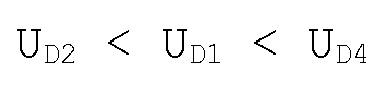
s'applique aux tensions de claquage (UD2, UD4, UD1) du premier (D2), du deuxième (D4) et du troisième (D1) dispositifs limiteurs de tension. - Circuit selon l'une des revendications précédentes,
caractérisé
en ce que l'inverseur est exécuté en tant que circuit en demi-pont, le point central du demi-pont représentant la source de tension alternative. - Circuit selon l'une des revendications 5 à 7,
caractérisé
en ce que le circuit comprend, en outre, un quatrième dispositif limiteur de tension (D8) qui est couplé entre la première résistance ohmique (R4) et le premier condensateur (C2), l'électrode de référence du quatrième commutateur électronique (T1) étant couplée au point de connexion de la première résistance ohmique (R4) et du quatrième dispositif limiteur de tension (D8), la sortie de la pompe de charge (D5, D6, C5), l'électrode de référence du premier commutateur électronique (T2) et l'électrode de référence du deuxième commutateur électronique (T4) étant couplées au point de connexion du quatrième dispositif limiteur de tension (D8) et du premier condensateur. - Circuit selon l'une des revendications précédentes,
caractérisé
en ce qu'un régulateur de tension (T3, C3, D3, R3) est couplé entre l'électrode de travail du premier commutateur électronique (T2) et le raccordement d'alimentation (V1) du dispositif de commande (MC). - Circuit selon l'une des revendications précédentes,
caractérisé
en ce qu'au moins le premier, le deuxième, le troisième et le quatrième dispositif limiteur de tension (D2, D4, D1, D8) est réalisé en tant que diode Zener. - Circuit selon l'une des revendications précédentes,
caractérisé
en ce que le premier dispositif limiteur de tension (D2) est couplé en série entre l'électrode de commande du premier commutateur électronique (T2) et l'électrode de travail du troisième commutateur électronique (T5). - Circuit selon l'une des revendications 1 à 10,
caractérisé
en ce qu'il comprend, en outre, une troisième résistance ohmique (R6) qui est couplée entre l'électrode de commande du premier commutateur électronique (T2) et l'électrode de travail du troisième commutateur électronique (T5), le troisième commutateur électronique (T5) étant exécuté en tant que MOSFET, le premier dispositif limiteur de tension (D2) étant couplé, d'une part, au point de connexion de la troisième résistance ohmique (R6) et de l'électrode de travail du troisième commutateur électronique (T5) et, d'autre part, au premier point de connexion. - Circuit selon l'une des revendications 1 à 11,
caractérisé
en ce qu'une quatrième résistance ohmique (R5) est couplée entre l'électrode de commande du troisième commutateur électronique (T5) et la sortie (A1) du dispositif de commande (MC). - Procédé de commutation d'une alimentation en courant pour un dispositif de commande (MC) dans un circuit comprenant un raccordement d'alimentation en tension continue (UZW) pour le raccordement à une source de tension continue et un raccordement d'alimentation en tension alternative (HBM) pour le raccordement à une source de tension alternative ;
caractérisé par les étapes suivantes :a) chargement d'un premier condensateur (C2) qui est couplé au raccordement d'alimentation en tension continue (UZW) par le biais d'une première résistance ohmique, formant un premier point de connexion ;b) lorsqu'on atteint un premier seuil de tension, pouvant être prédéfini, de la tension aux bornes du premier condensateur (C2) qui est plus élevé que la tension minimale de démarrage d'un circuit de commande (HBD) destiné à commander les commutateurs d'un inverseur, le raccordement d'alimentation en tension alternative (HBM) étant couplé à un potentiel de tension alternative alimenté par l'inverseur ; et ainsi ;
activation du circuit de commande (HBD) et, ainsi, fourniture d'une tension alternative aux bornes du raccordement d'alimentation en tension alternative (HBM) ;c) lorsqu'on atteint un second seuil de tension, pouvant être prédéfini, de la tension aux bornes du premier condensateur (C2) qui est supérieur au premier seuil de tension pouvant être prédéfini :
mise à l'état conducteur du trajet électrode de référence - électrode de travail d'un premier commutateur électronique (T4), le raccordement d'alimentation (V1) du dispositif de commande (MC) et au moins un consommateur supplémentaire (OP ; DR) étant couplés à l'électrode de travail du premier commutateur électronique, l'électrode de référence du premier commutateur électronique (T4) étant couplée au premier point de connexion ;d) établissement d'un état pour commuter l'alimentation en courant du dispositif de commande (MC) ;e) mise à l'état conducteur d'un deuxième commutateur électronique (T2), couplé à la sortie (A1) du dispositif de commande (MC), qui est couplé en série entre le premier point de connexion et le raccordement d'alimentation (V1) du dispositif de commande (MC) ; et
blocage de la tension aux bornes du premier condensateur (C2) au moyen d'un dispositif limiteur de tension (D2) à une valeur qui est inférieure à la tension minimale de démarrage du circuit de commande (HBD), et ainsi :désactivation du circuit de commande (HBD) ; etmise à l'état non conducteur du premier commutateur électronique (T4) .
Applications Claiming Priority (1)
| Application Number | Priority Date | Filing Date | Title |
|---|---|---|---|
| PCT/EP2007/062391 WO2009062554A1 (fr) | 2007-11-15 | 2007-11-15 | Alimentation en courant commutable pour circuits auxiliaires dans un convertisseur |
Publications (2)
| Publication Number | Publication Date |
|---|---|
| EP2208400A1 EP2208400A1 (fr) | 2010-07-21 |
| EP2208400B1 true EP2208400B1 (fr) | 2011-04-13 |
Family
ID=39810225
Family Applications (1)
| Application Number | Title | Priority Date | Filing Date |
|---|---|---|---|
| EP20070822633 Not-in-force EP2208400B1 (fr) | 2007-11-15 | 2007-11-15 | Alimentation en courant commutable pour circuits auxiliaires dans un convertisseur |
Country Status (7)
| Country | Link |
|---|---|
| US (1) | US8299647B2 (fr) |
| EP (1) | EP2208400B1 (fr) |
| KR (1) | KR20100096175A (fr) |
| CN (1) | CN101999254B (fr) |
| AT (1) | ATE505937T1 (fr) |
| DE (1) | DE502007006967D1 (fr) |
| WO (1) | WO2009062554A1 (fr) |
Cited By (1)
| Publication number | Priority date | Publication date | Assignee | Title |
|---|---|---|---|---|
| EP3586435A1 (fr) * | 2017-02-22 | 2020-01-01 | EBM-PAPST Landshut GmbH | Arrêt de veille |
Families Citing this family (5)
| Publication number | Priority date | Publication date | Assignee | Title |
|---|---|---|---|---|
| CA2768518A1 (fr) * | 2009-08-21 | 2011-02-24 | Osram Sylvania Inc. | Onduleur resonant dote d'un circuit de veille |
| FR2955434B1 (fr) * | 2010-01-21 | 2012-08-17 | Comtec Tech | Dispositif sans pile avec moyens de communication sans fil et procede de gestion de l'alimentation en courant electrique de ces moyens de communication |
| CN104704147B (zh) | 2012-05-28 | 2017-06-30 | 水吉能公司 | 电解器与能量系统 |
| US9966847B2 (en) * | 2015-07-17 | 2018-05-08 | Bose Corporation | Adaptive fail-save power-on control circuit |
| DE102019206692A1 (de) * | 2019-05-09 | 2020-11-12 | Robert Bosch Gmbh | Anlaufschaltung, Ansteuerschaltung und Verfahren zur Spannungsversorgung einer Steuervorrichtung |
Family Cites Families (5)
| Publication number | Priority date | Publication date | Assignee | Title |
|---|---|---|---|---|
| US4704542A (en) | 1985-03-22 | 1987-11-03 | Rca Corporation | Standby power supply |
| DE19542012A1 (de) * | 1995-11-10 | 1997-05-15 | Hugh Himmelsbach | Netzgespeiste Schaltungsanordnung zum Betrieb von Niederdruckentladungslampen, insbesondere Leuchtstofflampen |
| DE10106438A1 (de) | 2001-02-09 | 2002-08-14 | Patent Treuhand Ges Fuer Elektrische Gluehlampen Mbh | Vorschaltgerät zum Betrieb von elektrischen Lampen |
| DE102004036522A1 (de) * | 2004-07-28 | 2006-03-23 | Infineon Technologies Ag | Ansteuerschaltung für einen Schalter in einem Schaltwandler zur Verbesserung der Sprungantwort |
| DE102005025626A1 (de) * | 2005-06-03 | 2006-12-07 | Patent-Treuhand-Gesellschaft für elektrische Glühlampen mbH | Elektronisches Vorschaltgerät für mindestens eine Lampe |
-
2007
- 2007-11-15 KR KR1020107013206A patent/KR20100096175A/ko not_active Ceased
- 2007-11-15 US US12/742,949 patent/US8299647B2/en not_active Expired - Fee Related
- 2007-11-15 WO PCT/EP2007/062391 patent/WO2009062554A1/fr not_active Ceased
- 2007-11-15 EP EP20070822633 patent/EP2208400B1/fr not_active Not-in-force
- 2007-11-15 CN CN200780101559.1A patent/CN101999254B/zh not_active Expired - Fee Related
- 2007-11-15 AT AT07822633T patent/ATE505937T1/de active
- 2007-11-15 DE DE200750006967 patent/DE502007006967D1/de active Active
Cited By (1)
| Publication number | Priority date | Publication date | Assignee | Title |
|---|---|---|---|---|
| EP3586435A1 (fr) * | 2017-02-22 | 2020-01-01 | EBM-PAPST Landshut GmbH | Arrêt de veille |
Also Published As
| Publication number | Publication date |
|---|---|
| US20100259103A1 (en) | 2010-10-14 |
| US8299647B2 (en) | 2012-10-30 |
| DE502007006967D1 (de) | 2011-05-26 |
| EP2208400A1 (fr) | 2010-07-21 |
| CN101999254B (zh) | 2014-09-17 |
| KR20100096175A (ko) | 2010-09-01 |
| ATE505937T1 (de) | 2011-04-15 |
| WO2009062554A1 (fr) | 2009-05-22 |
| CN101999254A (zh) | 2011-03-30 |
Similar Documents
| Publication | Publication Date | Title |
|---|---|---|
| DE102011087368B4 (de) | Treiberschaltung, Anordnung und Verfahren zum Bootstrapping eines Schaltertreibers | |
| DE112014006951B4 (de) | Kurzschluss-Schutzschaltung für Halbleiterelemente vom Typ mit Lichtbogen-Selbstlöschung | |
| DE102007002731B4 (de) | Lichtstromkreis | |
| DE69103918T2 (de) | Synchronschaltsystem verwendender Leistungswandler mit hohem Wirkungsgrad. | |
| DE102011087434A1 (de) | Anordnung und Verfahren zum Treiben eines Schalters | |
| DE4208894A1 (de) | Schaltung zur ansteuerung eines spannungsgesteuerten halbleiterschalters | |
| EP0060336A2 (fr) | Procédé pour la commande d'un transistor de puissance du type FET et circuits pour la mise en oeuvre de ce procédé | |
| EP2208400B1 (fr) | Alimentation en courant commutable pour circuits auxiliaires dans un convertisseur | |
| EP0062276B1 (fr) | Ballast pour le fonctionnement de lampes à décharge à basse pression | |
| DE102011087431A1 (de) | Anordnung und Verfahren zum Treiben eines Kaskodenschalters | |
| EP2446526B1 (fr) | Circuiterie pour faire fonctionner au moins une diode électroluminescente (del) | |
| DE2809439A1 (de) | Schaltungseinrichtung zur steuerung des basisstromes eines als schalttransistor betriebenen leistungstransistors | |
| EP3748827A1 (fr) | Convertisseur demi-pont avec tension de grille reduite pendant les temps morts | |
| EP1299933A2 (fr) | Circuit electronique pour appareil d'alimentation en energie, notamment pour chargeur de batteries | |
| EP0219074A2 (fr) | Commutateur du type à deux fils avec un transistor de puissance | |
| DE19837728A1 (de) | Schaltungsanordnung zum Betrieb mindestens einer Entladungslampe | |
| EP3317967B1 (fr) | Circuit de commutation destiné à la commande d'un transistor | |
| EP0259845B1 (fr) | Protection contre l'inversion de polarité et contre les tensions alternatives pour les consommateurs électriques à courant continu | |
| EP1396925B1 (fr) | Circuit de charge pour un convertisseur | |
| EP1738618B1 (fr) | Circuit d'attaque pour convertisseur | |
| DE2555541C3 (de) | Netz-Batterie-Umschaltung für elektronische Geräte | |
| EP0122907A1 (fr) | Circuit de commande pour transistor de commutation | |
| EP1862885A2 (fr) | Circuit destiné à la mise en circuit à faible perte d'un moniteur lors de l'allumage d'un ordinateur et procédé correspondant | |
| DE3208449A1 (de) | Treiberschaltung fuer einen transistor | |
| EP1484947B1 (fr) | Circuit interrupteur pour commander une lampe |
Legal Events
| Date | Code | Title | Description |
|---|---|---|---|
| PUAI | Public reference made under article 153(3) epc to a published international application that has entered the european phase |
Free format text: ORIGINAL CODE: 0009012 |
|
| 17P | Request for examination filed |
Effective date: 20100312 |
|
| AK | Designated contracting states |
Kind code of ref document: A1 Designated state(s): AT BE BG CH CY CZ DE DK EE ES FI FR GB GR HU IE IS IT LI LT LU LV MC MT NL PL PT RO SE SI SK TR |
|
| AX | Request for extension of the european patent |
Extension state: AL BA HR MK RS |
|
| GRAP | Despatch of communication of intention to grant a patent |
Free format text: ORIGINAL CODE: EPIDOSNIGR1 |
|
| DAX | Request for extension of the european patent (deleted) | ||
| GRAS | Grant fee paid |
Free format text: ORIGINAL CODE: EPIDOSNIGR3 |
|
| GRAA | (expected) grant |
Free format text: ORIGINAL CODE: 0009210 |
|
| AK | Designated contracting states |
Kind code of ref document: B1 Designated state(s): AT BE BG CH CY CZ DE DK EE ES FI FR GB GR HU IE IS IT LI LT LU LV MC MT NL PL PT RO SE SI SK TR |
|
| REG | Reference to a national code |
Ref country code: GB Ref legal event code: FG4D Free format text: NOT ENGLISH |
|
| REG | Reference to a national code |
Ref country code: CH Ref legal event code: EP |
|
| REG | Reference to a national code |
Ref country code: CH Ref legal event code: NV Representative=s name: SIEMENS SCHWEIZ AG |
|
| REG | Reference to a national code |
Ref country code: IE Ref legal event code: FG4D Free format text: LANGUAGE OF EP DOCUMENT: GERMAN |
|
| REF | Corresponds to: |
Ref document number: 502007006967 Country of ref document: DE Date of ref document: 20110526 Kind code of ref document: P |
|
| REG | Reference to a national code |
Ref country code: DE Ref legal event code: R096 Ref document number: 502007006967 Country of ref document: DE Effective date: 20110526 |
|
| REG | Reference to a national code |
Ref country code: NL Ref legal event code: VDEP Effective date: 20110413 |
|
| REG | Reference to a national code |
Ref country code: SE Ref legal event code: TRGR |
|
| LTIE | Lt: invalidation of european patent or patent extension |
Effective date: 20110413 |
|
| PG25 | Lapsed in a contracting state [announced via postgrant information from national office to epo] |
Ref country code: PT Free format text: LAPSE BECAUSE OF FAILURE TO SUBMIT A TRANSLATION OF THE DESCRIPTION OR TO PAY THE FEE WITHIN THE PRESCRIBED TIME-LIMIT Effective date: 20110816 Ref country code: LT Free format text: LAPSE BECAUSE OF FAILURE TO SUBMIT A TRANSLATION OF THE DESCRIPTION OR TO PAY THE FEE WITHIN THE PRESCRIBED TIME-LIMIT Effective date: 20110413 |
|
| REG | Reference to a national code |
Ref country code: IE Ref legal event code: FD4D |
|
| PG25 | Lapsed in a contracting state [announced via postgrant information from national office to epo] |
Ref country code: SI Free format text: LAPSE BECAUSE OF FAILURE TO SUBMIT A TRANSLATION OF THE DESCRIPTION OR TO PAY THE FEE WITHIN THE PRESCRIBED TIME-LIMIT Effective date: 20110413 Ref country code: ES Free format text: LAPSE BECAUSE OF FAILURE TO SUBMIT A TRANSLATION OF THE DESCRIPTION OR TO PAY THE FEE WITHIN THE PRESCRIBED TIME-LIMIT Effective date: 20110724 Ref country code: LV Free format text: LAPSE BECAUSE OF FAILURE TO SUBMIT A TRANSLATION OF THE DESCRIPTION OR TO PAY THE FEE WITHIN THE PRESCRIBED TIME-LIMIT Effective date: 20110413 Ref country code: CY Free format text: LAPSE BECAUSE OF FAILURE TO SUBMIT A TRANSLATION OF THE DESCRIPTION OR TO PAY THE FEE WITHIN THE PRESCRIBED TIME-LIMIT Effective date: 20110413 Ref country code: IS Free format text: LAPSE BECAUSE OF FAILURE TO SUBMIT A TRANSLATION OF THE DESCRIPTION OR TO PAY THE FEE WITHIN THE PRESCRIBED TIME-LIMIT Effective date: 20110813 Ref country code: GR Free format text: LAPSE BECAUSE OF FAILURE TO SUBMIT A TRANSLATION OF THE DESCRIPTION OR TO PAY THE FEE WITHIN THE PRESCRIBED TIME-LIMIT Effective date: 20110714 Ref country code: FI Free format text: LAPSE BECAUSE OF FAILURE TO SUBMIT A TRANSLATION OF THE DESCRIPTION OR TO PAY THE FEE WITHIN THE PRESCRIBED TIME-LIMIT Effective date: 20110413 |
|
| PG25 | Lapsed in a contracting state [announced via postgrant information from national office to epo] |
Ref country code: NL Free format text: LAPSE BECAUSE OF FAILURE TO SUBMIT A TRANSLATION OF THE DESCRIPTION OR TO PAY THE FEE WITHIN THE PRESCRIBED TIME-LIMIT Effective date: 20110413 |
|
| PG25 | Lapsed in a contracting state [announced via postgrant information from national office to epo] |
Ref country code: IE Free format text: LAPSE BECAUSE OF FAILURE TO SUBMIT A TRANSLATION OF THE DESCRIPTION OR TO PAY THE FEE WITHIN THE PRESCRIBED TIME-LIMIT Effective date: 20110413 Ref country code: EE Free format text: LAPSE BECAUSE OF FAILURE TO SUBMIT A TRANSLATION OF THE DESCRIPTION OR TO PAY THE FEE WITHIN THE PRESCRIBED TIME-LIMIT Effective date: 20110413 Ref country code: CZ Free format text: LAPSE BECAUSE OF FAILURE TO SUBMIT A TRANSLATION OF THE DESCRIPTION OR TO PAY THE FEE WITHIN THE PRESCRIBED TIME-LIMIT Effective date: 20110413 |
|
| REG | Reference to a national code |
Ref country code: DE Ref legal event code: R081 Ref document number: 502007006967 Country of ref document: DE Owner name: OSRAM GMBH, DE Free format text: FORMER OWNER: OSRAM GESELLSCHAFT MIT BESCHRAENKTER HAFTUNG, 81543 MUENCHEN, DE Effective date: 20111214 |
|
| PLBE | No opposition filed within time limit |
Free format text: ORIGINAL CODE: 0009261 |
|
| STAA | Information on the status of an ep patent application or granted ep patent |
Free format text: STATUS: NO OPPOSITION FILED WITHIN TIME LIMIT |
|
| PG25 | Lapsed in a contracting state [announced via postgrant information from national office to epo] |
Ref country code: PL Free format text: LAPSE BECAUSE OF FAILURE TO SUBMIT A TRANSLATION OF THE DESCRIPTION OR TO PAY THE FEE WITHIN THE PRESCRIBED TIME-LIMIT Effective date: 20110413 Ref country code: SK Free format text: LAPSE BECAUSE OF FAILURE TO SUBMIT A TRANSLATION OF THE DESCRIPTION OR TO PAY THE FEE WITHIN THE PRESCRIBED TIME-LIMIT Effective date: 20110413 Ref country code: RO Free format text: LAPSE BECAUSE OF FAILURE TO SUBMIT A TRANSLATION OF THE DESCRIPTION OR TO PAY THE FEE WITHIN THE PRESCRIBED TIME-LIMIT Effective date: 20110413 Ref country code: DK Free format text: LAPSE BECAUSE OF FAILURE TO SUBMIT A TRANSLATION OF THE DESCRIPTION OR TO PAY THE FEE WITHIN THE PRESCRIBED TIME-LIMIT Effective date: 20110413 |
|
| 26N | No opposition filed |
Effective date: 20120116 |
|
| REG | Reference to a national code |
Ref country code: DE Ref legal event code: R097 Ref document number: 502007006967 Country of ref document: DE Effective date: 20120116 |
|
| BERE | Be: lapsed |
Owner name: OSRAM G.M.B.H. Effective date: 20111130 |
|
| PG25 | Lapsed in a contracting state [announced via postgrant information from national office to epo] |
Ref country code: MC Free format text: LAPSE BECAUSE OF NON-PAYMENT OF DUE FEES Effective date: 20111130 |
|
| PG25 | Lapsed in a contracting state [announced via postgrant information from national office to epo] |
Ref country code: BE Free format text: LAPSE BECAUSE OF NON-PAYMENT OF DUE FEES Effective date: 20111130 |
|
| PGFP | Annual fee paid to national office [announced via postgrant information from national office to epo] |
Ref country code: CH Payment date: 20121122 Year of fee payment: 6 |
|
| PG25 | Lapsed in a contracting state [announced via postgrant information from national office to epo] |
Ref country code: MT Free format text: LAPSE BECAUSE OF FAILURE TO SUBMIT A TRANSLATION OF THE DESCRIPTION OR TO PAY THE FEE WITHIN THE PRESCRIBED TIME-LIMIT Effective date: 20110413 |
|
| PGFP | Annual fee paid to national office [announced via postgrant information from national office to epo] |
Ref country code: IT Payment date: 20121121 Year of fee payment: 6 Ref country code: GB Payment date: 20121120 Year of fee payment: 6 Ref country code: SE Payment date: 20121120 Year of fee payment: 6 |
|
| REG | Reference to a national code |
Ref country code: DE Ref legal event code: R081 Ref document number: 502007006967 Country of ref document: DE Owner name: OSRAM GMBH, DE Free format text: FORMER OWNER: OSRAM AG, 81543 MUENCHEN, DE Effective date: 20130205 |
|
| PG25 | Lapsed in a contracting state [announced via postgrant information from national office to epo] |
Ref country code: LU Free format text: LAPSE BECAUSE OF NON-PAYMENT OF DUE FEES Effective date: 20111115 |
|
| PG25 | Lapsed in a contracting state [announced via postgrant information from national office to epo] |
Ref country code: BG Free format text: LAPSE BECAUSE OF FAILURE TO SUBMIT A TRANSLATION OF THE DESCRIPTION OR TO PAY THE FEE WITHIN THE PRESCRIBED TIME-LIMIT Effective date: 20110713 |
|
| PG25 | Lapsed in a contracting state [announced via postgrant information from national office to epo] |
Ref country code: TR Free format text: LAPSE BECAUSE OF FAILURE TO SUBMIT A TRANSLATION OF THE DESCRIPTION OR TO PAY THE FEE WITHIN THE PRESCRIBED TIME-LIMIT Effective date: 20110413 |
|
| REG | Reference to a national code |
Ref country code: DE Ref legal event code: R081 Ref document number: 502007006967 Country of ref document: DE Owner name: OSRAM GMBH, DE Free format text: FORMER OWNER: OSRAM GMBH, 81543 MUENCHEN, DE Effective date: 20130823 |
|
| PG25 | Lapsed in a contracting state [announced via postgrant information from national office to epo] |
Ref country code: HU Free format text: LAPSE BECAUSE OF FAILURE TO SUBMIT A TRANSLATION OF THE DESCRIPTION OR TO PAY THE FEE WITHIN THE PRESCRIBED TIME-LIMIT Effective date: 20110413 |
|
| REG | Reference to a national code |
Ref country code: AT Ref legal event code: MM01 Ref document number: 505937 Country of ref document: AT Kind code of ref document: T Effective date: 20121130 |
|
| PG25 | Lapsed in a contracting state [announced via postgrant information from national office to epo] |
Ref country code: AT Free format text: LAPSE BECAUSE OF NON-PAYMENT OF DUE FEES Effective date: 20121130 |
|
| REG | Reference to a national code |
Ref country code: CH Ref legal event code: PL |
|
| REG | Reference to a national code |
Ref country code: SE Ref legal event code: EUG |
|
| GBPC | Gb: european patent ceased through non-payment of renewal fee |
Effective date: 20131115 |
|
| PG25 | Lapsed in a contracting state [announced via postgrant information from national office to epo] |
Ref country code: CH Free format text: LAPSE BECAUSE OF NON-PAYMENT OF DUE FEES Effective date: 20131130 Ref country code: LI Free format text: LAPSE BECAUSE OF NON-PAYMENT OF DUE FEES Effective date: 20131130 |
|
| PG25 | Lapsed in a contracting state [announced via postgrant information from national office to epo] |
Ref country code: SE Free format text: LAPSE BECAUSE OF NON-PAYMENT OF DUE FEES Effective date: 20131116 Ref country code: IT Free format text: LAPSE BECAUSE OF NON-PAYMENT OF DUE FEES Effective date: 20131115 |
|
| PG25 | Lapsed in a contracting state [announced via postgrant information from national office to epo] |
Ref country code: GB Free format text: LAPSE BECAUSE OF NON-PAYMENT OF DUE FEES Effective date: 20131115 |
|
| REG | Reference to a national code |
Ref country code: FR Ref legal event code: PLFP Year of fee payment: 9 |
|
| REG | Reference to a national code |
Ref country code: FR Ref legal event code: PLFP Year of fee payment: 10 |
|
| PGFP | Annual fee paid to national office [announced via postgrant information from national office to epo] |
Ref country code: FR Payment date: 20161118 Year of fee payment: 10 |
|
| REG | Reference to a national code |
Ref country code: FR Ref legal event code: ST Effective date: 20180731 |
|
| PG25 | Lapsed in a contracting state [announced via postgrant information from national office to epo] |
Ref country code: FR Free format text: LAPSE BECAUSE OF NON-PAYMENT OF DUE FEES Effective date: 20171130 |
|
| PGFP | Annual fee paid to national office [announced via postgrant information from national office to epo] |
Ref country code: DE Payment date: 20181120 Year of fee payment: 12 |
|
| REG | Reference to a national code |
Ref country code: DE Ref legal event code: R119 Ref document number: 502007006967 Country of ref document: DE |
|
| PG25 | Lapsed in a contracting state [announced via postgrant information from national office to epo] |
Ref country code: DE Free format text: LAPSE BECAUSE OF NON-PAYMENT OF DUE FEES Effective date: 20200603 |