EP2209251B1 - Appareil et procédé de traitement cryptographique - Google Patents
Appareil et procédé de traitement cryptographique Download PDFInfo
- Publication number
- EP2209251B1 EP2209251B1 EP09176232.8A EP09176232A EP2209251B1 EP 2209251 B1 EP2209251 B1 EP 2209251B1 EP 09176232 A EP09176232 A EP 09176232A EP 2209251 B1 EP2209251 B1 EP 2209251B1
- Authority
- EP
- European Patent Office
- Prior art keywords
- gate
- output
- arithmetic
- bit string
- function
- Prior art date
- Legal status (The legal status is an assumption and is not a legal conclusion. Google has not performed a legal analysis and makes no representation as to the accuracy of the status listed.)
- Not-in-force
Links
Images


Classifications
-
- H—ELECTRICITY
- H04—ELECTRIC COMMUNICATION TECHNIQUE
- H04L—TRANSMISSION OF DIGITAL INFORMATION, e.g. TELEGRAPHIC COMMUNICATION
- H04L9/00—Cryptographic mechanisms or cryptographic arrangements for secret or secure communications; Network security protocols
- H04L9/06—Cryptographic mechanisms or cryptographic arrangements for secret or secure communications; Network security protocols the encryption apparatus using shift registers or memories for block-wise or stream coding, e.g. DES systems or RC4; Hash functions; Pseudorandom sequence generators
- H04L9/0618—Block ciphers, i.e. encrypting groups of characters of a plain text message using fixed encryption transformation
- H04L9/0625—Block ciphers, i.e. encrypting groups of characters of a plain text message using fixed encryption transformation with splitting of the data block into left and right halves, e.g. Feistel based algorithms, DES, FEAL, IDEA or KASUMI
-
- H—ELECTRICITY
- H04—ELECTRIC COMMUNICATION TECHNIQUE
- H04L—TRANSMISSION OF DIGITAL INFORMATION, e.g. TELEGRAPHIC COMMUNICATION
- H04L2209/00—Additional information or applications relating to cryptographic mechanisms or cryptographic arrangements for secret or secure communication H04L9/00
- H04L2209/12—Details relating to cryptographic hardware or logic circuitry
- H04L2209/122—Hardware reduction or efficient architectures
Definitions
- the embodiment(s) described herein relate to a cryptographic processing apparatus and a cryptographic processing method.
- cipher algorithms are utilized as fundamental technologies of security systems.
- cipher algorithms are classified into two groups, namely, public key cryptosystems and common key cryptosystems.
- the public key cryptosystems use different keys for encryption and decryption.
- the public key cryptosystems keep a key for decrypting ciphertext called a secret key as secret information only for a receiver, instead of making a key for encryption called a public key publicly available, to thereby ensure high security.
- the common key cryptosystems use the same key for encryption and decryption called a common key.
- the common key cryptosystems keep a common key as information unknown to any third party other than the sender and receiver to thereby ensure high security.
- the cipher algorithms of the common key cryptosystems have the advantages of high processing speed and compact packaging over the cipher algorithms of the public key cryptosystems. Therefore, the encryption function is added to compact devices such as mobile phones or integrated-circuit (IC) cards using the cipher algorithms of the common key cryptosystems. Furthermore, due to the high processing speed and real-time encryption/decryption of information, the cipher algorithms of the common key cryptosystems are also used for broadcasting or information communication in communication fields.
- the cipher algorithms of the common key cryptosystems are classified into two types, namely, stream ciphers and block ciphers.
- the block ciphers are widely used in terms of security.
- the block ciphers divide plaintext into blocks each having a certain bit length, and encrypt the plaintext block by block.
- the bit length of each block which is the unit of encryption is called "block length”.
- MISTY1 is described in, for example, Specification of MISTY1 ( ⁇ http://www.cryptrec.go.jp/cryptrec_03_spec_cypherlist-files/PDF/05_02jspec. pdf>).
- MISTY1 is a cipher algorithm with a common key size of 128 bits and a block length of 64 bits. That is, MISTY1 generates 64-bit ciphertext from 64-bit plaintext using a 128-bit common key. In the following, a description will be given of a round processing part of MISTY1.
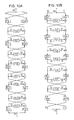
- Figs. 10A and 10B are circuit diagrams illustrating an example configuration of a MISTY1 round processing part.
- Fig. 10A illustrates a round processing part for use in the decryption process.
- Fig. 10B illustrates a round processing part for use in the encryption process.
- the round processing part of MISTY1 illustrated in Figs. 10A and 10B performs processing where the number of rounds n is 8. In Specification of MISTY1 mentioned above, 8 rounds are recommended.
- the round processing part of MISTY1 has a Feistel structure with eight FO functions FO1 FO2, FO3, FO4 FO5, FO6, FO7, and FO8 and ten FL functions FL1, FL2, FL3, FL4, FL5, FL6, FL7, FL8, FL9, and FL10 or ten FL -1 functions FL1 -1 , FL2 -1 , FL3 -1 , FL4 -1 , FL5 -1 , FL6 - 1 , FL7 -1 , FL8 -1 , FL9 -1 , and FL10 -1 .
- 64-bit plaintext P is input and 64-bit ciphertext C is output.
- 64-bit ciphertext C is input and 64-bit plaintext P is output.
- Fig. 11A is a circuit diagram illustrating an example configuration of an FL function.
- Fig. 11B is a circuit diagram illustrating an example configuration of an FL -1 function.
- the FL function includes an AND gate 1a in the first stage and an OR gate 2a in the second stage.
- the FL -1 function includes an OR gate 2b in the first stage and an AND gate 1b in the second stage.
- KL ij (1 ⁇ i ⁇ 8, 1 ⁇ j ⁇ 2) represents 16-bit data at the j-th position from the left of KL i , where KL i denotes an extended key.
- extended-key processing is performed to generate a 256-bit extended key KL i from a 128-bit secret key K. The details of the generation of an extended key are described in Specification of MISTY1 mentioned above.
- the bit string of the upper 16 bits of the 32-bit input and the upper 16 bits KL i1 of the extended key are input to the AND gate 1a.
- the bit string of the lower 16 bits of the 32-bit input and the output of the AND gate 1a are input to an XOR gate 3a.
- the output of the XOR gate 3a and the lower 16 bits KL i2 of the extended key are input to the OR gate 2a.
- the bit string of the upper 16 bits of the 32-bit input and the output of the OR gate 2a are input to an XOR gate 3b.
- the output of the XOR gate 3b corresponds to the upper 16 bits of a 32-bit output of the FL function
- the output of the XOR gate 3a corresponds to the lower 16 bits of the 32-bit output of the FL function.
- the bit string of the lower 16 bits of the 32-bit input and the lower 16 bits KL i2 of the extended key are input to the OR gate 2b.
- the bit string of the upper 16 bits of the 32-bit input and the output of the OR gate 2b are input to an XOR gate 3c.
- the output of the XOR gate 3c and the upper 16 bits KL i1 of the extended key are input to the AND gate 1b.
- the bit string of the lower 16 bits of the 32-bit input and the output of the AND gate 1b are input to an XOR gate 3d.
- the output of the XOR gate 3c corresponds to the upper 16 bits of a 32-bit output of the FL -1 function
- the output of the XOR gate 3d corresponds to the lower 16 bits of the 32-bit output of the FL -1 function.
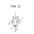
- FIG. 12 is a circuit diagram illustrating an implementation method in the first typical example.
- an FL function 6 and an FL -1 function 7 can be switched using a selector 5 depending on the encryption process or the decryption process.
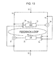
- FIG. 13 is a circuit diagram illustrating an implementation method in the second typical example.
- a single AND gate 1c and a single OR gate 2c are used for implementation.
- an AND gate and an OR gate which are common parts between the two functions, are shared and the functions are merged into a single function.
- bit string of the lower 16 bits of a 32-bit input and the output of the AND gate 1c are input to an XOR gate 3e.
- the bit string of the upper 16 bits of the 32-bit input and the output of the OR gate 2c are input to an XOR gate 3f.
- the bit string of the upper 16 bits of the 32-bit input and the output of the XOR gate 3f are input to a selector 5a.
- the bit string of the lower 16 bits of the 32-bit input and the output of the XOR gate 3e are input to a selector 5b.
- the output of the selector 5a and the upper 16 bits KL i1 of an extended key are input to the AND gate 1c.
- the output of the selector 5b and the lower 16 bits KL i2 of the extended key are input to the OR gate 2c.
- the output of the XOR gate 3f corresponds to the upper 16 bits of a 32-bit output of the circuit illustrated in Fig. 13
- the output of the XOR gate 3e corresponds to the lower 16 bits of the 32-bit output of the circuit illustrated in Fig. 13 .
- the circuit illustrated in Fig. 13 serves as an FL function.
- the circuit serves as an FL -1 function.
- This technique allows a significant reduction in circuit size.
- a related technique is disclosed in Dai Yamamoto, et al., "A Very Compact Hardware Implementation of the MISTY1 Block Cipher", CHES 2008, LNCS 5154, pp. 315-330, 2008 , or Akashi Satoh and Sumio Morioka, "Small and High-Speed Hardware Architectures for the 3GPP Standard Cipher KASUMI", Information Security Conference 2002, LNCS 2433, pp. 48-62, 2002 .
- EP1978496 discloses a process configuration for a Feistel cipher in which the number of rounds may be easily changed.
- the process configuration has an SP type round function F which includes a non linear conversion section S and a linear conversion section P.
- Menezes, Vanstone, Orschot, "Handbook of applied Cryptography", 1997, CRC Press LLC, USA discloses a Feistel structure in which the inner function F may be a product cipher.
- EP0790595 discloses a data transformation apparatus and method for encryption, decryption of input data.
- the cryptographic processing apparatus includes a first arithmetic gate configured to receive a first input bit string and a first extended key bit string, the first input bit string being an upper N-bit string in a 2N-bit input of the cryptographic processing apparatus, where the first extended key bit string is based on one of an upper N-bit string and a lower N-bit string of an extended key, the first arithmetic gate is one of an AND gate and an OR gate.
- a cryptographic processing apparatus includes a first XOR gate configured to receive an output of the first arithmetic gate and a second input bit string, the second input bit string being a lower N-bit string in the 2N-bit input of the cryptographic processing apparatus; a second arithmetic gate configured to receive an output of the first XOR gate and a second extended key bit string, the second extended key bit string being based on the other of the upper N-bit string and the lower N-bit string of the extended key, the second arithmetic gate being a gate different from the first arithmetic gate and the other of the AND gate and the OR gate; a second XOR gate configured to receive an output of the second arithmetic gate and the first input bit string; a third arithmetic gate configured to receive an output of the second XOR gate and the first extended key bit string, the third arithmetic gate being a same gate as the first arithmetic gate and the one of the AND gate and the OR gate; and
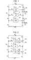
- Fig. 1 is a circuit diagram illustrating an example configuration of a merge function according to a first example embodying the present invention.
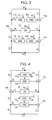
- Fig. 2 is a circuit diagram illustrating an example configuration of a merge function according to a second example embodying the present invention.
- Fig. 3 is a circuit diagram illustrating an example configuration of a merge function according to a third example embodying the present invention.
- Fig. 4 is a circuit diagram illustrating an example configuration of a merge function according to a fourth example embodying the present invention.
- Fig. 5 is a circuit diagram illustrating an example configuration of a merge function according to a fifth example embodying the present invention.
- Fig. 6 is a circuit diagram illustrating an example configuration of a merge function according to a sixth example embodying the present invention.
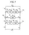
- Fig. 7 is a circuit diagram illustrating an example configuration of a merge function according to a seventh example embodying the present invention.
- Fig. 8 is a table illustrating exemplary circuit sizes according to embodiment(s).
- Fig. 9 is a table illustrating exemplary delay times according to embodiment(s).
- Fig. 10A is a circuit diagram illustrating an example configuration of a round processing part for performing decryption according to MISTY1.
- Fig. 10B is a circuit diagram illustrating an example configuration of a round processing part for performing encryption according to MISTY1.
- Fig. 11A is a circuit diagram illustrating an example configuration of an FL function.
- Fig. 11B is a circuit diagram illustrating an example configuration of an FL -1 function.
- Fig. 12 is a circuit diagram illustrating an implementation method in a first typical example.
- Fig. 13 is a circuit diagram illustrating an implementation method in a second typical example.
- the second typical example has a serious problem in that a feedback loop is formed in a combinational circuit. Regardless of which function the circuit illustrated in Fig. 13 serves as, no registers are included in a path and a loop structure is formed only in a combinational circuit.
- logic synthesis which is an operation for conversion from a hardware description language into a circuit structure.
- Even if it is possible to perform logic synthesis there is a risk that a circuit generated after the conversion may be an oscillator circuit. Therefore, in terms of reliability, it is difficult to commercialize a circuit having the feedback loop structure described above into a product.
- the FL function and the FL -1 function are merged to produce a single function, it is not easy to achieve a reduction in circuit size without forming a feedback loop in a circuit configuration. Therefore, in many developments pertaining to MISTY1 and KASUMI, as in the first typical example, the FL function and the FL -1 function are independently implemented.
- the present technique has been carried out in order to overcome the problems or difficulties described above and others existing in typical systems, and provides a cryptographic processing apparatus for realizing a merge function including an FL function and an FL -1 function using a circuit having no feedback loop.
- the present technique provides a compact hardware implementation in common key cryptosystems that employ an FL function and an FL -1 function, such as MISTY1, MISTY2, KASUMI, and CAMELLIA, by using a new function obtained by efficiently merging the FL function and the FL -1 function into a single function.
- the present technique is useful for producing compact common key cipher hardware.
- a merge function obtained by merging an FL function and an FL -1 function into a single function will be described in the context of MISTY1 by way of example.
- the basic concept of application to MISTY2, KASUMI, CAMELLIA, and the like is similar to that for MISTY1. While particular applications are discussed herein, embodiments of the present invention are not limited to implementation with any specific methodology, technique or specific algorithm related to cryptography.
- Fig. 1 is a circuit diagram illustrating an example configuration of a merge function according to a first example.
- an FL function is configured using a circuit having a two-stage structure in which an AND gate is provided in the first stage and an OR gate is provided in the second stage.
- an FL -1 function is configured using a function having a two-stage structure in which an OR gate is provided in the first stage and an AND gate is provided in the second stage.
- the merge function according to the first example is configured using a circuit having a three-stage structure.
- the merge function according to the first example is configured using a circuit including a first arithmetic gate corresponding to an AND gate 11a in the first stage, a second arithmetic gate corresponding to an OR gate 12 in the second stage, and a third arithmetic gate corresponding to an AND gate 11b in the third stage.
- a circuit including a first arithmetic gate corresponding to an AND gate 11a in the first stage, a second arithmetic gate corresponding to an OR gate 12 in the second stage, and a third arithmetic gate corresponding to an AND gate 11b in the third stage.
- the OR gate 12 is common to the two functions.
- a 32-bit input of the circuit illustrated in Fig. 1 is divided into a first input bit string corresponding to the input upper bit string of the upper 16 bits and a second input bit string corresponding to the input lower bit string of the lower 16 bits.
- N 16.
- the input upper bit string and a first extended key bit string KL i1 corresponding to the upper 16 bits of an extended key are input to the AND gate 11a.
- the input lower bit string and the output of the AND gate 11a are input to a first XOR gate corresponding to an XOR gate 13a.
- the output of the XOR gate 13a and the input lower bit string are input to a first selector corresponding to a selector 14a.
- the output of the selector 14a and a second extended key bit string KL i2 corresponding to the lower 16 bits of the extended key are input to the OR gate 12.
- the input upper bit string and the output of the OR gate 12 are input to a second XOR gate corresponding to an XOR gate 13b.
- the output of the XOR gate 13b and KL i1 are input to the AND gate 11b.
- the output of the selector 14a and the output of the AND gate 11b are input to a third XOR gate corresponding to an XOR gate 13c.
- the output of the XOR gate 13c and the output of the selector 14a are input to a second selector corresponding to a selector 14b.
- the output of the XOR gate 13b corresponds to the upper 16 bits of a 32-bit output of the circuit illustrated in Fig. 1 .
- the output of the selector 14b corresponds to the lower 16 bits of the 32-bit output of the circuit.
- each of the selectors 14a and 14b selects and outputs one of the two inputs in accordance with a selection signal sel.
- the selector 14a selects the output of the XOR gate 13a
- the selector 14b selects the output of the selector 14a.
- the circuit illustrated in Fig. 1 serves as an FL function.
- the selector 14a selects the input lower bit string
- the selector 14b selects the output of the XOR gate 13c. Accordingly, the circuit illustrated in Fig. 1 serves as an FL -1 function.
- OR gate 12 rather than both an AND gate and an OR gate, is used as a common part, thereby avoiding the formation of a feedback loop.
- the FL function and the FL -1 function are merged into a single function, leading to saving of and thereby the circuit size corresponding to a 16-bit AND gate and a 16-bit XOR gate, that is, 56 gates, can be removed. Therefore, the first typical example requires a circuit size of about 336 gates for 0.18-micrometer process while the first example requires a circuit size of about 280 gates.
- the selectors in the first example are equivalently transformed into AND gates.
- Fig. 2 is a circuit diagram illustrating an example configuration of a merge function according to a second example.
- the same reference numerals as those in Fig. 1 represent the same portions as or equivalent portions to those illustrated in Fig. 1 , and will not be described here.
- the selectors 14a and 14b in the circuit illustrated in Fig. 1 are moved to the input side of the XOR gates 13a and 13c to obtain a third selector corresponding to a selector 15a and a fourth selector corresponding to a selector 15b, respectively. Therefore, the selectors 15a and 15b can select the output signals of the AND gates 11a and 11b, respectively, or 0 signal of 16 bits.
- the selector 15a upon receipt of a selection signal corresponding to the FL function, the selector 15a selects the output of the AND gate 11a, and the selector 15b selects the 0 signal. Accordingly, the circuit illustrated in Fig. 2 serves as an FL function.
- the selector 15a upon receipt of a selection signal corresponding to the FL -1 function, the selector 15a selects the 0 signal, and the selector 15b selects the output of the AND gate 11b. Accordingly, the circuit illustrated in Fig. 2 serves as an FL -1 function.
- Fig. 3 is a circuit diagram illustrating an example configuration of a merge function according to a third example.
- the same reference numerals as those in Fig. 2 represent the same portions as or equivalent portions to those illustrated in Fig. 2 , and will not be described here.
- the selectors 15a and 15b in the circuit illustrated in Fig. 2 are equivalently transformed into a first AND gate corresponding to an AND gate 16a and a second AND gate corresponding to an AND gate 16b, respectively.
- the selection signals sel for the selectors are 1-bit signals
- selection signals sel are 16-bit expanded signals.
- the AND gate 16a performs an AND operation between the output of the AND gate 11a and the selection signal sel.
- the AND gate 16b performs an AND operation between the output of the AND gate 11b and the negation of the selection signal sel.
- the merging of the FL function and the FL -1 function into a single function may cause an extension of the critical path, leading to a reduction in processing speed.
- a 2-1 NAND gate has a delay d.
- the delays of the individual gates are 2d, 2d, 3d, and 3d, respectively.
- the delay of the critical path in the first typical example illustrated in Fig. 12 is given by the sum of the delay of FL or FL -1 and the delay of the selector that selects FL or FL -1 .
- Fig. 4 is a circuit diagram illustrating an example configuration of a merge function according to a fourth example.
- the same reference numerals as those in Fig. 3 represent the same portions as or equivalent portions to those illustrated in Fig. 3 , and will not be described here.
- the AND gates 16a and 16b in the circuit illustrated in Fig. 3 are removed from the critical path and are replaced by a third AND gate corresponding to an AND gate 17a and a fourth AND gate corresponding to an AND gate 17b, respectively.
- the AND gate 17a performs an AND operation between a selection signal sel and KL i1 .
- the AND gate 17b performs an AND operation between the negation of the selection signal sel and KL i1 .
- a path for generating an extended key KL ij is not a critical path. This is because there are a large number of known implementations capable of generating KL ij in a cycle preceding the processing cycle of the FL function.
- the application of those implementations to MISTY1 can prevent the effect of the delay time for generating the extended key KL ij on the delay time of the FL function.
- the AND gates 16a and 16b illustrated in Fig. 3 can be moved to the positions of the AND gates 17a and 17b illustrated in Fig. 4 . Therefore, the delay of the critical path in the circuit illustrated in Fig. 4 can be reduced by an amount corresponding to two AND gates, as compared with that in the circuit illustrated in Fig.
- Fig. 5 is a circuit diagram illustrating an example configuration of a merge function according to a fifth example.
- the same reference numerals as those in Fig. 1 represent the same portions as or equivalent portions to those illustrated in Fig. 1 , and will not be described here.
- the fifth example has a basic configuration and advantages similar to those in the first example illustrated in Fig. 1 , but is different in the arrangement of OR gates and an AND gate.
- an OR gate is common to the FL function and the FL -1 function
- an AND gate is common to the FL function and the FL -1 function. More specifically, the circuit illustrated in Fig.
- FIG. 5 is configured using a circuit including a first arithmetic gate corresponding to an OR gate 21a in the first stage, a second arithmetic gate corresponding to an AND gate 22 in the second stage, and a third arithmetic gate corresponding to an OR gate 21b in the third stage.
- a circuit including a first arithmetic gate corresponding to an OR gate 21a in the first stage, a second arithmetic gate corresponding to an AND gate 22 in the second stage, and a third arithmetic gate corresponding to an OR gate 21b in the third stage.
- only the AND gate 22 is common to the two functions.
- a first extended key bit string corresponds to the input of an OR gate based on KL i2
- a second extended key bit string corresponds to the input of an AND gate based on KL i1 .
- Fig. 6 is a circuit diagram illustrating an example configuration of a merge function according to the sixth example.
- the same reference numerals as those in Fig. 5 represent the same portions as or equivalent portions to those illustrated in Fig. 5 , and will not be described here.
- the selectors 14a and 14b in the circuit illustrated in Fig. 5 are moved to the input side of the XOR gates 13a and 13c to obtain selectors 15a and 15b, respectively.
- the sixth example has a basic configuration and advantages similar to those of the second example, but is different in the arrangement of OR gates and an AND gate.
- Fig. 7 is a circuit diagram illustrating an example configuration of a merge function according to the seventh example.
- the same reference numerals as those in Fig. 6 represent the same portions as or equivalent portions to those illustrated in Fig. 6 , and will not be described here.
- the selectors 15a and 15b in the circuit illustrated in Fig. 6 are equivalently transformed into AND gates 16a and 16b, respectively.
- the seventh example has a basic configuration and advantages similar to those in the third example, but is different in the arrangement of OR gates and an AND gate.
- Fig. 8 is a table illustrating exemplary circuit sizes of the circuits according to the respective examples.
- the table illustrated in Fig. 8 provides exemplary circuit sizes in the first to seventh examples and the first and second typical examples.
- #1-bit MUX represents the number of selectors having a width of 1 bit.
- #1-bit AND/OR represents the number of AND gates and OR gates having a width of 1 bit.
- #1-bit XOR represents the number of XOR gates having a width of 1 bit.
- Gate Count represents the circuit size concerning the FL function and the FL -1 function. In the first typical example, the circuit size is as large as 336 gates.
- the second typical example allows a small circuit size; however, due to the use of the feedback loop structure, the implementation cannot be commercialized into a product.
- the first and second examples allow a reduction in circuit size as compared with the first typical example, but have small advantages. This is because the circuit sizes of the selectors are the same.
- the third and fourth examples allow a reduction in circuit size up to 200 gates by equivalently transforming the selectors in the first example into AND gates.
- the circuit size concerning the FL function and the FL -1 function is reduced from 336 gates to 200 gates, that is, by about 40%.
- the overall circuit size of a typical compact MISTY1 hardware implementation is about 4000 gates for 0.18-micrometer process according to Yamamoto et al. in the paper mentioned above.
- the application of the fourth example to this typical technique allows a reduction in circuit size by about 3.5%.
- the overall circuit size of a typical compact KASUMI hardware implementation is about 3400 gates for 0.13-micrometer process according to Satoh and Morioka in the paper mentioned above.
- the application of the fourth example to this typical technique allows a reduction in circuit size by up to 4%.
- Fig. 9 is a table illustrating exemplary delay times in the respective examples.
- the table illustrated in Fig. 9 provides exemplary delay times in the first to seventh examples and the first and second typical examples.
- AND/OR represents the number of AND gates and OR gates in the merge function.
- XOR represents a number of XOR gates in a merge function.
- 2-1MUX represents the number of selectors in the merge function.
- Delay represents the delay time of the merge function. In the first typical example, the delay time is 13d. In the first example, in contrast, the delay time is larger and is 21d. This is because, as described previously, the merge function has a three-stage structure, and additional selectors are generated within the merge function.
- the equivalent transformation of the selectors into AND gates allows a reduction in delay time by 2d but the delay time is still larger than that in the first typical example.
- the removal of the two AND gates from the critical path results in a delay time of 15d. Therefore, the delay time in the fourth example is substantially equivalent to that in the first typical example, i.e., 13d.
- one of an AND gate and an OR gate is used as a common module to merge the functions, thereby avoiding the formation of a feedback loop.
- the selectors which may cause the increase in circuit size and the extension of the critical path, are equivalently transformed into AND gates, thereby reducing the circuit size. Further, the AND gates are removed from the critical path, thereby reducing the critical path. While the configurations and structures of the embodiment(s) herein are described using specific examples, the present invention is not limited to particulars of any of the examples.
- the embodiments can be implemented in computing hardware (computing apparatus) and/or software, such as (in a non-limiting example) any computer that can store, retrieve, process and/or output data and/or communicate with other computers.
- the results produced can be displayed on a display of the computing hardware.
- a program/software implementing the embodiments may be recorded on computer-readable media comprising computer-readable recording media.
- the program/software implementing the embodiments may also be transmitted over transmission communication media.
- Examples of the computer-readable recording media include a magnetic recording apparatus, an optical disk, a magneto-optical disk, and/or a semiconductor memory (for example, RAM, ROM, etc.).
- Examples of the magnetic recording apparatus include a hard disk device (HDD), a flexible disk (FD), and a magnetic tape (MT).
- optical disk examples include a DVD (Digital Versatile Disc), a DVD-RAM, a CD-ROM (Compact Disc - Read Only Memory), and a CD-R (Recordable)/RW.
- communication media includes a carrier-wave signal.
Landscapes
- Engineering & Computer Science (AREA)
- Computer Security & Cryptography (AREA)
- Computer Networks & Wireless Communication (AREA)
- Signal Processing (AREA)
- Logic Circuits (AREA)
- Storage Device Security (AREA)
- Semiconductor Integrated Circuits (AREA)
Claims (14)
- Appareil de traitement cryptographique pour exécuter une opération arithmétique dans un processus cryptographique, l'appareil de traitement comprenant :une première porte arithmétique (11a, 21a) configurée pour recevoir une première chaîne de bits d'entrée et une première chaîne de bits de clé étendue (KLi1), la première chaîne de bits d'entrée étant une chaîne de N bits supérieure dans une entrée de 2N bits de l'appareil de traitement cryptographique, la première chaîne de bits de clé étendue (KLi1) étant basée sur l'une d'une chaîne de N bits supérieure et d'une chaîne de N bits inférieure d'une clé étendue, la première porte arithmétique étant l'une d'une porte ET (11a) et d'une porte OU (21a) ;une première porte OU exclusif (13 a) configurée pour recevoir une sortie de la première porte arithmétique (11a, 21a) et une deuxième chaîne de bits d'entrée, la deuxième chaîne de bits d'entrée étant une chaîne de N bits inférieure dans l'entrée de 2N bits de l'appareil de traitement cryptographique ;une deuxième porte arithmétique (12, 22) configurée pour recevoir une sortie de la première porte OU exclusif (13a) et une deuxième chaîne de bits de clé étendue (KL2), la chaîne de bits de clé étendue (KL2) étant basée sur l'autre de la chaîne de N bits supérieure et de la chaîne de N bits inférieure de la clé étendue, la deuxième porte arithmétique (12, 22) étant une porte différente de la première porte arithmétique (11a, 21a) et de l'autre de la porte ET (22) et de la porte OU (12) ;une deuxième porte OU exclusif (13b) configurée pour recevoir une sortie de la deuxième porte arithmétique (12, 22) et la première chaîne de bits d'entrée ;une troisième porte arithmétique (11b, 21b) configurée pour recevoir une sortie de la deuxième porte OU exclusif (13b) et la première chaîne de bits de clé étendue, la troisième porte arithmétique (11b, 21b) étant une porte identique à la première porte arithmétique (11a, 21a) et à ladite une de la porte ET (11b) et de la porte OU (21 b) ; etune troisième porte OU exclusif (13c) configurée pour recevoir une sortie de la troisième porte arithmétique (11b, 21b) et une sortie de la première porte OU exclusif (13a),dans lequel l'appareil de traitement est apte à servir de fonction FL ou bien de fonction FL-1, où une fonction FL comporte une porte ET dans un premier étage et une porte OU dans un deuxième étage et une fonction FL-1 comprend une porte OU dans un premier étage et une porte ET dans un deuxième étage.
- Appareil de traitement cryptographique selon la revendication 1, comprenant en outre :un premier sélecteur (14a) configuré pour sélectionner l'une de la sortie de la première porte OU exclusif (13a) et de la deuxième chaîne de bits d'entrée sur la base d'un signal de sélection reçu, et pour envoyer ce qui a été sélectionné à la deuxième porte arithmétique (12, 22) et la troisième porte OU exclusif (13c) ; etun deuxième sélecteur (14b) configuré pour sélectionner l'une d'une sortie de la troisième porte OU exclusif (13c) sur la base du signal de sélection, et d'une sortie du premier sélecteur (14a), et pour émettre ce qui a été sélectionné.
- Appareil de traitement cryptographique selon la revendication 2, dans lequel le premier sélecteur (14a) est configuré pour sélectionner la sortie de la première porte OU exclusif (13a) lors de la réception d'un signal de sélection correspondant à la fonction FL et pour sélectionner la deuxième chaîne de bits d'entrée lors de la réception d'un signal de sélection correspondant à la fonction FL-1, et
dans lequel le deuxième sélecteur (14b) est configuré pour sélectionner la sortie du premier sélecteur (14a) lors de la réception du signal de sélection correspondant à la fonction FL et pour sélectionner la sortie de la troisième porte OU exclusif (13c) lors de la réception du signal de sélection correspondant à la fonction FL-1. - Appareil de traitement cryptographique selon l'une quelconque des revendications 1 à 3, comprenant en outre :un troisième sélecteur (15a) configuré pour sélectionner l'un de la sortie de la première porte arithmétique (11a, 21a) et d'un signal nul de N bits sur la base d'un signal de sélection reçu, et pour envoyer ce qui a été sélectionné à la première porte OU exclusif (13a) ; etun quatrième sélecteur (15b) configuré pour sélectionner l'un de la sortie de la troisième porte arithmétique (11b, 21b) et d'un signal nul de N bits sur la base du signal de sélection, et pour envoyer ce qui a été sélectionné à la troisième porte OU exclusif (13c).
- Appareil de traitement cryptographique selon la revendication 4, dans lequel le troisième sélecteur (15a) est configuré pour sélectionner la sortie de la première porte arithmétique (11a, 21a) lors de la réception d'un signal de sélection correspondant à la fonction FL et pour sélectionner le signal nul de N bits lors de la réception d'un signal de sélection correspondant à la fonction FL-1, et
dans lequel le quatrième sélecteur (15b) est configuré pour sélectionner le signal nul de N bits lors de la réception du signal de sélection correspondant à la fonction FL et pour sélectionner la sortie de la troisième porte arithmétique (11b, 21b) lors de la réception du signal de sélection correspondant à la fonction FL-1. - Appareil de traitement cryptographique selon l'une quelconque des revendications 2 à 5, comprenant en outre :une première porte ET (16a) configurée pour exécuter une opération ET entre la sortie de la première porte arithmétique (11a, 21a) et le signal de sélection et pour envoyer un résultat à la première porte OU exclusif (13a) ; etune deuxième porte ET (16b) configurée pour exécuter une opération ET entre la sortie de la troisième porte arithmétique (11b, 21b) et une négation du signal de sélection et pour envoyer un résultat à la troisième porte OU exclusif (13c).
- Appareil de traitement cryptographique selon l'une quelconque des revendications 2 à 6, comprenant en outre :une troisième porte ET (17a) configurée pour exécuter une opération ET entre la chaîne de N bits supérieure (KLi1) de la clé étendue et le signal de sélection et pour envoyer un résultat à la première porte arithmétique (11a) ; etune quatrième porte ET (17b) configurée pour exécuter une opération ET entre la chaîne de N bits supérieure (KLi1) de la clé étendue et une négation du signal de sélection et pour envoyer un résultat à la troisième porte arithmétique (11b),dans lequel chacune de la première porte arithmétique (11a) et de la troisième porte arithmétique est une porte ET (11b), etla deuxième porte arithmétique (12) est une porte OU.
- Appareil de traitement cryptographique selon l'une quelconque des revendications 1 à 6, dans lequel chacune de la première porte arithmétique (21a) et de la troisième porte arithmétique (21b) est une porte OU, et
la deuxième porte arithmétique (22) est une porte ET. - Appareil de traitement cryptographique selon l'une quelconque des revendications 1 à 8, dans lequel la première porte arithmétique (11a, 21a), la première porte OU exclusif (13a), la deuxième porte arithmétique (12, 22), la deuxième porte OU exclusif (13b), la troisième porte arithmétique (11b, 21b) et la troisième porte OU exclusif (13c) sont prévues dans une fonction FL et une fonction FL-1 dans l'un ou l'autre d'un algorithme de chiffrement MISTY1, MISTY2, KASUMI ou CAMELLIA d'un cryptosystème à clé commune.
- Procédé de traitement cryptographique pour l'exécution d'une opération arithmétique dans un processus cryptographique, le procédé de traitement comprenant :l'application d'une première chaîne de bits d'entrée et d'une première chaîne de bits de clé étendue (KLi1) à l'entrée d'une première porte arithmétique (11a, 21a), la première chaîne de bits d'entrée étant une chaîne de N bits supérieure dans une entrée de 2N bits dans le procédé de traitement cryptographique, la première chaîne de bits de clé étendue (KLi1) étant basée sur l'une d'une chaîne de N bits supérieure et d'une chaîne de N bits inférieure d'une clé étendue, la première porte arithmétique (11a, 21a) étant l'une d'une porte ET (11a) et d'une porte OU (21a) ;l'application d'une sortie de la première porte arithmétique (11a, 21a) et d'une deuxième chaîne de bits d'entrée à l'entrée d'une première porte OU exclusif (13a), la deuxième chaîne de bits d'entrée étant une chaîne de N bits inférieure dans l'entrée de 2N bits dans le procédé de traitement cryptographique ;l'application d'une sortie de la première porte OU exclusif (13a) et d'une deuxième chaîne de bits de clé étendue (KLi2) à l'entrée d'une deuxième porte arithmétique (12, 22), la deuxième chaîne de bits de clé étendue (KLi2) étant basée sur l'autre de la chaîne de N bits supérieure et de la chaîne de N bits inférieure de la clé étendue, la deuxième porte arithmétique (12, 22) étant une porte différente de la première porte arithmétique (11a, 21a) et de l'autre de la porte ET (22) et de la porte OU (12) ;l'application d'une sortie de la deuxième porte arithmétique (12, 22) et de la première chaîne de bits d'entrée à l'entrée d'une deuxième porte OU exclusif (13b) ;l'application d'une sortie de la deuxième porte OU exclusif (13b) et la première chaîne de bits de clé étendue (KLi1) à l'entrée d'une troisième porte arithmétique (11b, 21b), la troisième porte arithmétique (11b, 21b) étant une porte identique à la première porte arithmétique (11, 21a) et à ladite une de la porte ET (11 b) et la porte OU (21 b) ; etl'application d'une sortie de la troisième porte arithmétique (11b, 21b) et d'une sortie de la première porte OU exclusif (13a) à l'entrée d'une troisième porte OU exclusif (13c),dans lequel le procédé de traitement est destiné à exécuter une fonction FL ou bien une fonction FL-1, où une fonction FL comporte une porte ET dans un premier étage et une porte OU dans un deuxième étage et une fonction FL-1 comprend une porte OU dans un premier étage et une porte ET dans un deuxième étage.
- Procédé de traitement cryptographique selon la revendication 10, comprenant en outre :l'application de la sortie de la première porte OU exclusif (13a) et de la deuxième chaîne de bits d'entrée à l'entrée d'un premier sélecteur (14a), le premier sélecteur (14a) étant configuré pour sélectionner l'une de deux entrées sur la base d'un signal de sélection reçu et pour envoyer l'entrée sélectionnée à la deuxième porte arithmétique (12, 22) et à la troisième porte OU exclusif (13c) ; etl'application d'une sortie de la troisième porte OU exclusif (13c) et d'une sortie du premier sélecteur (14a) à l'entrée un deuxième sélecteur (14b), le deuxième sélecteur (14b) étant configuré pour sélectionner l'une de deux sorties sur la base du signal de sélection et pour émettre la sortie sélectionnée.
- Procédé de traitement cryptographique selon la revendication 11, dans lequel le premier sélecteur (14a) sélectionne la sortie de la première porte OU exclusif (13a) lors de la réception d'un signal de sélection correspondant à la fonction FL, et sélectionne la deuxième chaîne de bits d'entrée lors de la réception d'un signal de sélection correspondant à la fonction FL-1, et
dans lequel le deuxième sélecteur (14b) sélectionne la sortie du premier sélecteur (14a) lors de la réception du signal de sélection correspondant à la fonction FL, et sélectionne la sortie de la troisième porte OU exclusif (13c) lors de la réception du signal de sélection correspondant à la fonction FL-1 . - Procédé de traitement cryptographique selon l'une quelconque des revendications 11 à 12, comprenant en outre :l'application de la sortie de la première porte arithmétique (11a, 21a) et d'un signal nul de N bits à l'entrée d'un troisième sélecteur (15a), le troisième sélecteur (15a) étant configuré pour sélectionner l'une de deux entrées sur la base d'un signal de sélection reçu et pour envoyer l'entrée sélectionnée à la première porte OU exclusif (13a) ; etl'application de la sortie de la troisième porte arithmétique (11b, 21b) et d'un signal nul de N bits à l'entrée d'un quatrième sélecteur (15b), le quatrième sélecteur (15b) étant configuré pour sélectionner l'une de deux entrées sur la base du signal de sélection et pour envoyer l'entrée sélectionnée à la troisième porte OU exclusif (13c).
- Procédé de traitement cryptographique selon la revendication 13, dans lequel le troisième sélecteur (15a) sélectionne la sortie de la première porte arithmétique (11a, 21a) lors de la réception d'un signal de sélection correspondant à la fonction FL, et sélectionne le signal nul de N bits lors de la réception d'un signal de sélection correspondant à la fonction FL-1, et
dans lequel le quatrième sélecteur (15b) sélectionne le signal nul de N bits lors de la réception du signal de sélection correspondant à la fonction FL, et sélectionne la sortie de la troisième porte arithmétique (11b, 21b) lors de la réception du signal de sélection correspondant à la fonction FL-1.
Applications Claiming Priority (1)
| Application Number | Priority Date | Filing Date | Title |
|---|---|---|---|
| JP2009007249A JP5200949B2 (ja) | 2009-01-16 | 2009-01-16 | 暗号処理装置 |
Publications (3)
| Publication Number | Publication Date |
|---|---|
| EP2209251A2 EP2209251A2 (fr) | 2010-07-21 |
| EP2209251A3 EP2209251A3 (fr) | 2012-02-22 |
| EP2209251B1 true EP2209251B1 (fr) | 2014-11-26 |
Family
ID=42135941
Family Applications (1)
| Application Number | Title | Priority Date | Filing Date |
|---|---|---|---|
| EP09176232.8A Not-in-force EP2209251B1 (fr) | 2009-01-16 | 2009-11-17 | Appareil et procédé de traitement cryptographique |
Country Status (3)
| Country | Link |
|---|---|
| US (1) | US8111827B2 (fr) |
| EP (1) | EP2209251B1 (fr) |
| JP (1) | JP5200949B2 (fr) |
Families Citing this family (7)
| Publication number | Priority date | Publication date | Assignee | Title |
|---|---|---|---|---|
| US8832464B2 (en) * | 2009-03-31 | 2014-09-09 | Oracle America, Inc. | Processor and method for implementing instruction support for hash algorithms |
| US9317286B2 (en) * | 2009-03-31 | 2016-04-19 | Oracle America, Inc. | Apparatus and method for implementing instruction support for the camellia cipher algorithm |
| US20100246815A1 (en) * | 2009-03-31 | 2010-09-30 | Olson Christopher H | Apparatus and method for implementing instruction support for the kasumi cipher algorithm |
| US20100250965A1 (en) * | 2009-03-31 | 2010-09-30 | Olson Christopher H | Apparatus and method for implementing instruction support for the advanced encryption standard (aes) algorithm |
| US8654970B2 (en) * | 2009-03-31 | 2014-02-18 | Oracle America, Inc. | Apparatus and method for implementing instruction support for the data encryption standard (DES) algorithm |
| JP5387295B2 (ja) * | 2009-09-29 | 2014-01-15 | 富士通株式会社 | 暗号装置及び方法 |
| GB201719355D0 (en) * | 2017-11-22 | 2018-01-03 | Univ Leuven Kath | Reconfigerable logic circuit |
Family Cites Families (7)
| Publication number | Priority date | Publication date | Assignee | Title |
|---|---|---|---|---|
| JPH04128395A (ja) | 1990-09-18 | 1992-04-28 | Nikkiso Co Ltd | ボイラ配管の腐食抑制における酸素ガス注入方法 |
| CN100435505C (zh) | 1995-09-05 | 2008-11-19 | 三菱电机株式会社 | 数据变换装置及数据变换方法 |
| US6185679B1 (en) * | 1998-02-23 | 2001-02-06 | International Business Machines Corporation | Method and apparatus for a symmetric block cipher using multiple stages with type-1 and type-3 feistel networks |
| CN100583192C (zh) * | 2000-03-09 | 2010-01-20 | 三菱电机株式会社 | 数据变换装置和数据变换方法 |
| JP4128395B2 (ja) * | 2002-05-23 | 2008-07-30 | 三菱電機株式会社 | データ変換装置 |
| JP2007177156A (ja) * | 2005-12-28 | 2007-07-12 | Ulvac Japan Ltd | 蛍光体及びその作製方法、並びに発光素子 |
| JP2007199156A (ja) | 2006-01-24 | 2007-08-09 | Sony Corp | 暗号処理装置、暗号処理装置製造装置、および方法、並びにコンピュータ・プログラム |
-
2009
- 2009-01-16 JP JP2009007249A patent/JP5200949B2/ja not_active Expired - Fee Related
- 2009-11-04 US US12/612,290 patent/US8111827B2/en not_active Expired - Fee Related
- 2009-11-17 EP EP09176232.8A patent/EP2209251B1/fr not_active Not-in-force
Also Published As
| Publication number | Publication date |
|---|---|
| US20100183143A1 (en) | 2010-07-22 |
| EP2209251A3 (fr) | 2012-02-22 |
| JP5200949B2 (ja) | 2013-06-05 |
| JP2010164792A (ja) | 2010-07-29 |
| EP2209251A2 (fr) | 2010-07-21 |
| US8111827B2 (en) | 2012-02-07 |
Similar Documents
| Publication | Publication Date | Title |
|---|---|---|
| US6246768B1 (en) | Data encryption system for encrypting plaintext data | |
| EP2209251B1 (fr) | Appareil et procédé de traitement cryptographique | |
| JP3864675B2 (ja) | 共通鍵暗号装置 | |
| US8396210B2 (en) | Cryptographic processing apparatus and cryptographic processing method, and computer program | |
| EP3123656B1 (fr) | Dispositif de traitement de chiffrement, procédé de traitement de chiffrement, et programme de commande | |
| JPWO2015146431A1 (ja) | 暗号処理装置、および暗号処理方法、並びにプログラム | |
| WO2004015916A1 (fr) | Dispositif et procede de cryptage/decryptage, dispositif et procede de cryptage, dispositif et procede de cryptage/decryptage et dispositif de transmission/reception | |
| KR20180081559A (ko) | 암호화 동작을 위한 키 시퀀스 생성 | |
| CN100382485C (zh) | 设计最优加密函数的方法和优化的加密设备 | |
| WO2015146430A1 (fr) | Dispositif de traitement de chiffrage, et procédé et programme de traitement de chiffrage | |
| JP2004157535A (ja) | データ暗号化方法 | |
| JP5056860B2 (ja) | データ変換関数の処理装置 | |
| Wang et al. | An ultra compact block cipher for serialized architecture implementations | |
| EP1629626B1 (fr) | Procede et appareil pour une implementation de la fonction d'extension de cle a faible utilisation de l'espace memoire | |
| Dichou et al. | Finding the best FPGA implementation of the DES algorithm to secure smart cards | |
| EP2209252B1 (fr) | Implantation compacte de chiffrements par blocs avec une structure de type MISTY | |
| Mancillas-López et al. | An Ultra-Fast Authenticated Encryption Scheme with Associated Data Using AES-OTR | |
| KR100494560B1 (ko) | Rijndael암호를 이용한 블록 데이터 실시간암호복호화 장치 및 방법 | |
| JP2004004603A (ja) | 拡大鍵生成装置、暗号化装置および暗号化システム | |
| US7583800B2 (en) | Encryption apparatus and method in a wireless communications system | |
| KR100668664B1 (ko) | Aes 라인달 블록 알고리즘을 이용하는 암호화/복호화장치 및 방법 | |
| Sasongko et al. | Architecture for the secret-key BC3 cryptography algorithm | |
| JP5929757B2 (ja) | 暗号処理装置および暗号処理方法 | |
| KR102348802B1 (ko) | Aes 암호화 및 복호화 회로 | |
| Howlader | Nonlinearity in AES Subkey Scheduling—An Augmented Security |
Legal Events
| Date | Code | Title | Description |
|---|---|---|---|
| PUAI | Public reference made under article 153(3) epc to a published international application that has entered the european phase |
Free format text: ORIGINAL CODE: 0009012 |
|
| AK | Designated contracting states |
Kind code of ref document: A2 Designated state(s): AT BE BG CH CY CZ DE DK EE ES FI FR GB GR HR HU IE IS IT LI LT LU LV MC MK MT NL NO PL PT RO SE SI SK SM TR |
|
| AX | Request for extension of the european patent |
Extension state: AL BA RS |
|
| PUAL | Search report despatched |
Free format text: ORIGINAL CODE: 0009013 |
|
| RIC1 | Information provided on ipc code assigned before grant |
Ipc: H04L 9/06 20060101AFI20120112BHEP |
|
| AK | Designated contracting states |
Kind code of ref document: A3 Designated state(s): AT BE BG CH CY CZ DE DK EE ES FI FR GB GR HR HU IE IS IT LI LT LU LV MC MK MT NL NO PL PT RO SE SI SK SM TR |
|
| AX | Request for extension of the european patent |
Extension state: AL BA RS |
|
| 17P | Request for examination filed |
Effective date: 20120816 |
|
| 17Q | First examination report despatched |
Effective date: 20130118 |
|
| GRAP | Despatch of communication of intention to grant a patent |
Free format text: ORIGINAL CODE: EPIDOSNIGR1 |
|
| INTG | Intention to grant announced |
Effective date: 20140618 |
|
| GRAS | Grant fee paid |
Free format text: ORIGINAL CODE: EPIDOSNIGR3 |
|
| GRAA | (expected) grant |
Free format text: ORIGINAL CODE: 0009210 |
|
| AK | Designated contracting states |
Kind code of ref document: B1 Designated state(s): AT BE BG CH CY CZ DE DK EE ES FI FR GB GR HR HU IE IS IT LI LT LU LV MC MK MT NL NO PL PT RO SE SI SK SM TR |
|
| REG | Reference to a national code |
Ref country code: GB Ref legal event code: FG4D |
|
| REG | Reference to a national code |
Ref country code: CH Ref legal event code: EP |
|
| REG | Reference to a national code |
Ref country code: AT Ref legal event code: REF Ref document number: 698704 Country of ref document: AT Kind code of ref document: T Effective date: 20141215 |
|
| REG | Reference to a national code |
Ref country code: IE Ref legal event code: FG4D |
|
| REG | Reference to a national code |
Ref country code: DE Ref legal event code: R096 Ref document number: 602009027942 Country of ref document: DE Effective date: 20141231 |
|
| REG | Reference to a national code |
Ref country code: NL Ref legal event code: VDEP Effective date: 20141126 |
|
| REG | Reference to a national code |
Ref country code: AT Ref legal event code: MK05 Ref document number: 698704 Country of ref document: AT Kind code of ref document: T Effective date: 20141126 |
|
| REG | Reference to a national code |
Ref country code: LT Ref legal event code: MG4D |
|
| PG25 | Lapsed in a contracting state [announced via postgrant information from national office to epo] |
Ref country code: PT Free format text: LAPSE BECAUSE OF FAILURE TO SUBMIT A TRANSLATION OF THE DESCRIPTION OR TO PAY THE FEE WITHIN THE PRESCRIBED TIME-LIMIT Effective date: 20150326 Ref country code: LT Free format text: LAPSE BECAUSE OF FAILURE TO SUBMIT A TRANSLATION OF THE DESCRIPTION OR TO PAY THE FEE WITHIN THE PRESCRIBED TIME-LIMIT Effective date: 20141126 Ref country code: IS Free format text: LAPSE BECAUSE OF FAILURE TO SUBMIT A TRANSLATION OF THE DESCRIPTION OR TO PAY THE FEE WITHIN THE PRESCRIBED TIME-LIMIT Effective date: 20150326 Ref country code: FI Free format text: LAPSE BECAUSE OF FAILURE TO SUBMIT A TRANSLATION OF THE DESCRIPTION OR TO PAY THE FEE WITHIN THE PRESCRIBED TIME-LIMIT Effective date: 20141126 Ref country code: NO Free format text: LAPSE BECAUSE OF FAILURE TO SUBMIT A TRANSLATION OF THE DESCRIPTION OR TO PAY THE FEE WITHIN THE PRESCRIBED TIME-LIMIT Effective date: 20150226 Ref country code: ES Free format text: LAPSE BECAUSE OF FAILURE TO SUBMIT A TRANSLATION OF THE DESCRIPTION OR TO PAY THE FEE WITHIN THE PRESCRIBED TIME-LIMIT Effective date: 20141126 Ref country code: NL Free format text: LAPSE BECAUSE OF FAILURE TO SUBMIT A TRANSLATION OF THE DESCRIPTION OR TO PAY THE FEE WITHIN THE PRESCRIBED TIME-LIMIT Effective date: 20141126 |
|
| PG25 | Lapsed in a contracting state [announced via postgrant information from national office to epo] |
Ref country code: CY Free format text: LAPSE BECAUSE OF FAILURE TO SUBMIT A TRANSLATION OF THE DESCRIPTION OR TO PAY THE FEE WITHIN THE PRESCRIBED TIME-LIMIT Effective date: 20141126 Ref country code: GR Free format text: LAPSE BECAUSE OF FAILURE TO SUBMIT A TRANSLATION OF THE DESCRIPTION OR TO PAY THE FEE WITHIN THE PRESCRIBED TIME-LIMIT Effective date: 20150227 Ref country code: AT Free format text: LAPSE BECAUSE OF FAILURE TO SUBMIT A TRANSLATION OF THE DESCRIPTION OR TO PAY THE FEE WITHIN THE PRESCRIBED TIME-LIMIT Effective date: 20141126 Ref country code: SE Free format text: LAPSE BECAUSE OF FAILURE TO SUBMIT A TRANSLATION OF THE DESCRIPTION OR TO PAY THE FEE WITHIN THE PRESCRIBED TIME-LIMIT Effective date: 20141126 Ref country code: LV Free format text: LAPSE BECAUSE OF FAILURE TO SUBMIT A TRANSLATION OF THE DESCRIPTION OR TO PAY THE FEE WITHIN THE PRESCRIBED TIME-LIMIT Effective date: 20141126 Ref country code: HR Free format text: LAPSE BECAUSE OF FAILURE TO SUBMIT A TRANSLATION OF THE DESCRIPTION OR TO PAY THE FEE WITHIN THE PRESCRIBED TIME-LIMIT Effective date: 20141126 |
|
| PG25 | Lapsed in a contracting state [announced via postgrant information from national office to epo] |
Ref country code: RO Free format text: LAPSE BECAUSE OF FAILURE TO SUBMIT A TRANSLATION OF THE DESCRIPTION OR TO PAY THE FEE WITHIN THE PRESCRIBED TIME-LIMIT Effective date: 20141126 Ref country code: SK Free format text: LAPSE BECAUSE OF FAILURE TO SUBMIT A TRANSLATION OF THE DESCRIPTION OR TO PAY THE FEE WITHIN THE PRESCRIBED TIME-LIMIT Effective date: 20141126 Ref country code: DK Free format text: LAPSE BECAUSE OF FAILURE TO SUBMIT A TRANSLATION OF THE DESCRIPTION OR TO PAY THE FEE WITHIN THE PRESCRIBED TIME-LIMIT Effective date: 20141126 Ref country code: CZ Free format text: LAPSE BECAUSE OF FAILURE TO SUBMIT A TRANSLATION OF THE DESCRIPTION OR TO PAY THE FEE WITHIN THE PRESCRIBED TIME-LIMIT Effective date: 20141126 Ref country code: EE Free format text: LAPSE BECAUSE OF FAILURE TO SUBMIT A TRANSLATION OF THE DESCRIPTION OR TO PAY THE FEE WITHIN THE PRESCRIBED TIME-LIMIT Effective date: 20141126 |
|
| REG | Reference to a national code |
Ref country code: DE Ref legal event code: R097 Ref document number: 602009027942 Country of ref document: DE |
|
| PG25 | Lapsed in a contracting state [announced via postgrant information from national office to epo] |
Ref country code: PL Free format text: LAPSE BECAUSE OF FAILURE TO SUBMIT A TRANSLATION OF THE DESCRIPTION OR TO PAY THE FEE WITHIN THE PRESCRIBED TIME-LIMIT Effective date: 20141126 |
|
| REG | Reference to a national code |
Ref country code: FR Ref legal event code: PLFP Year of fee payment: 7 |
|
| PLBE | No opposition filed within time limit |
Free format text: ORIGINAL CODE: 0009261 |
|
| STAA | Information on the status of an ep patent application or granted ep patent |
Free format text: STATUS: NO OPPOSITION FILED WITHIN TIME LIMIT |
|
| 26N | No opposition filed |
Effective date: 20150827 |
|
| PG25 | Lapsed in a contracting state [announced via postgrant information from national office to epo] |
Ref country code: IT Free format text: LAPSE BECAUSE OF FAILURE TO SUBMIT A TRANSLATION OF THE DESCRIPTION OR TO PAY THE FEE WITHIN THE PRESCRIBED TIME-LIMIT Effective date: 20141126 |
|
| PG25 | Lapsed in a contracting state [announced via postgrant information from national office to epo] |
Ref country code: SI Free format text: LAPSE BECAUSE OF FAILURE TO SUBMIT A TRANSLATION OF THE DESCRIPTION OR TO PAY THE FEE WITHIN THE PRESCRIBED TIME-LIMIT Effective date: 20141126 |
|
| PG25 | Lapsed in a contracting state [announced via postgrant information from national office to epo] |
Ref country code: LU Free format text: LAPSE BECAUSE OF FAILURE TO SUBMIT A TRANSLATION OF THE DESCRIPTION OR TO PAY THE FEE WITHIN THE PRESCRIBED TIME-LIMIT Effective date: 20151117 Ref country code: MC Free format text: LAPSE BECAUSE OF FAILURE TO SUBMIT A TRANSLATION OF THE DESCRIPTION OR TO PAY THE FEE WITHIN THE PRESCRIBED TIME-LIMIT Effective date: 20141126 |
|
| REG | Reference to a national code |
Ref country code: CH Ref legal event code: PL |
|
| PG25 | Lapsed in a contracting state [announced via postgrant information from national office to epo] |
Ref country code: LI Free format text: LAPSE BECAUSE OF NON-PAYMENT OF DUE FEES Effective date: 20151130 Ref country code: CH Free format text: LAPSE BECAUSE OF NON-PAYMENT OF DUE FEES Effective date: 20151130 |
|
| REG | Reference to a national code |
Ref country code: IE Ref legal event code: MM4A |
|
| REG | Reference to a national code |
Ref country code: FR Ref legal event code: PLFP Year of fee payment: 8 |
|
| PG25 | Lapsed in a contracting state [announced via postgrant information from national office to epo] |
Ref country code: IE Free format text: LAPSE BECAUSE OF NON-PAYMENT OF DUE FEES Effective date: 20151117 |
|
| PG25 | Lapsed in a contracting state [announced via postgrant information from national office to epo] |
Ref country code: BG Free format text: LAPSE BECAUSE OF FAILURE TO SUBMIT A TRANSLATION OF THE DESCRIPTION OR TO PAY THE FEE WITHIN THE PRESCRIBED TIME-LIMIT Effective date: 20141126 Ref country code: HU Free format text: LAPSE BECAUSE OF FAILURE TO SUBMIT A TRANSLATION OF THE DESCRIPTION OR TO PAY THE FEE WITHIN THE PRESCRIBED TIME-LIMIT; INVALID AB INITIO Effective date: 20091117 |
|
| PG25 | Lapsed in a contracting state [announced via postgrant information from national office to epo] |
Ref country code: SM Free format text: LAPSE BECAUSE OF NON-PAYMENT OF DUE FEES Effective date: 20141126 |
|
| PG25 | Lapsed in a contracting state [announced via postgrant information from national office to epo] |
Ref country code: MT Free format text: LAPSE BECAUSE OF FAILURE TO SUBMIT A TRANSLATION OF THE DESCRIPTION OR TO PAY THE FEE WITHIN THE PRESCRIBED TIME-LIMIT Effective date: 20141126 Ref country code: TR Free format text: LAPSE BECAUSE OF FAILURE TO SUBMIT A TRANSLATION OF THE DESCRIPTION OR TO PAY THE FEE WITHIN THE PRESCRIBED TIME-LIMIT Effective date: 20141126 |
|
| PG25 | Lapsed in a contracting state [announced via postgrant information from national office to epo] |
Ref country code: BE Free format text: LAPSE BECAUSE OF FAILURE TO SUBMIT A TRANSLATION OF THE DESCRIPTION OR TO PAY THE FEE WITHIN THE PRESCRIBED TIME-LIMIT Effective date: 20141126 |
|
| REG | Reference to a national code |
Ref country code: FR Ref legal event code: PLFP Year of fee payment: 9 |
|
| PGFP | Annual fee paid to national office [announced via postgrant information from national office to epo] |
Ref country code: FR Payment date: 20171012 Year of fee payment: 9 Ref country code: DE Payment date: 20171114 Year of fee payment: 9 |
|
| PGFP | Annual fee paid to national office [announced via postgrant information from national office to epo] |
Ref country code: GB Payment date: 20171115 Year of fee payment: 9 |
|
| PG25 | Lapsed in a contracting state [announced via postgrant information from national office to epo] |
Ref country code: MK Free format text: LAPSE BECAUSE OF FAILURE TO SUBMIT A TRANSLATION OF THE DESCRIPTION OR TO PAY THE FEE WITHIN THE PRESCRIBED TIME-LIMIT Effective date: 20141126 |
|
| REG | Reference to a national code |
Ref country code: DE Ref legal event code: R119 Ref document number: 602009027942 Country of ref document: DE |
|
| GBPC | Gb: european patent ceased through non-payment of renewal fee |
Effective date: 20181117 |
|
| PG25 | Lapsed in a contracting state [announced via postgrant information from national office to epo] |
Ref country code: FR Free format text: LAPSE BECAUSE OF NON-PAYMENT OF DUE FEES Effective date: 20181130 Ref country code: DE Free format text: LAPSE BECAUSE OF NON-PAYMENT OF DUE FEES Effective date: 20190601 |
|
| PG25 | Lapsed in a contracting state [announced via postgrant information from national office to epo] |
Ref country code: GB Free format text: LAPSE BECAUSE OF NON-PAYMENT OF DUE FEES Effective date: 20181117 |