EP2210073B1 - Circuiterie pour la production de signaux dépendant de la luminosité et de la température, notamment pour un pyromètre produisant des images - Google Patents
Circuiterie pour la production de signaux dépendant de la luminosité et de la température, notamment pour un pyromètre produisant des images Download PDFInfo
- Publication number
- EP2210073B1 EP2210073B1 EP08846593.5A EP08846593A EP2210073B1 EP 2210073 B1 EP2210073 B1 EP 2210073B1 EP 08846593 A EP08846593 A EP 08846593A EP 2210073 B1 EP2210073 B1 EP 2210073B1
- Authority
- EP
- European Patent Office
- Prior art keywords
- sensor elements
- circuit arrangement
- wavelength range
- sensor
- electromagnetic radiation
- Prior art date
- Legal status (The legal status is an assumption and is not a legal conclusion. Google has not performed a legal analysis and makes no representation as to the accuracy of the status listed.)
- Active
Links
Images

Classifications
-
- G—PHYSICS
- G01—MEASURING; TESTING
- G01J—MEASUREMENT OF INTENSITY, VELOCITY, SPECTRAL CONTENT, POLARISATION, PHASE OR PULSE CHARACTERISTICS OF INFRARED, VISIBLE OR ULTRAVIOLET LIGHT; COLORIMETRY; RADIATION PYROMETRY
- G01J5/00—Radiation pyrometry, e.g. infrared or optical thermometry
- G01J5/60—Radiation pyrometry, e.g. infrared or optical thermometry using determination of colour temperature
-
- G—PHYSICS
- G01—MEASURING; TESTING
- G01J—MEASUREMENT OF INTENSITY, VELOCITY, SPECTRAL CONTENT, POLARISATION, PHASE OR PULSE CHARACTERISTICS OF INFRARED, VISIBLE OR ULTRAVIOLET LIGHT; COLORIMETRY; RADIATION PYROMETRY
- G01J5/00—Radiation pyrometry, e.g. infrared or optical thermometry
- G01J5/60—Radiation pyrometry, e.g. infrared or optical thermometry using determination of colour temperature
- G01J5/602—Radiation pyrometry, e.g. infrared or optical thermometry using determination of colour temperature using selective, monochromatic or bandpass filtering
-
- H—ELECTRICITY
- H10—SEMICONDUCTOR DEVICES; ELECTRIC SOLID-STATE DEVICES NOT OTHERWISE PROVIDED FOR
- H10F—INORGANIC SEMICONDUCTOR DEVICES SENSITIVE TO INFRARED RADIATION, LIGHT, ELECTROMAGNETIC RADIATION OF SHORTER WAVELENGTH OR CORPUSCULAR RADIATION
- H10F30/00—Individual radiation-sensitive semiconductor devices in which radiation controls the flow of current through the devices, e.g. photodetectors
- H10F30/20—Individual radiation-sensitive semiconductor devices in which radiation controls the flow of current through the devices, e.g. photodetectors the devices having potential barriers, e.g. phototransistors
- H10F30/21—Individual radiation-sensitive semiconductor devices in which radiation controls the flow of current through the devices, e.g. photodetectors the devices having potential barriers, e.g. phototransistors the devices being sensitive to infrared, visible or ultraviolet radiation
- H10F30/22—Individual radiation-sensitive semiconductor devices in which radiation controls the flow of current through the devices, e.g. photodetectors the devices having potential barriers, e.g. phototransistors the devices being sensitive to infrared, visible or ultraviolet radiation the devices having only one potential barrier, e.g. photodiodes
- H10F30/221—Individual radiation-sensitive semiconductor devices in which radiation controls the flow of current through the devices, e.g. photodetectors the devices having potential barriers, e.g. phototransistors the devices being sensitive to infrared, visible or ultraviolet radiation the devices having only one potential barrier, e.g. photodiodes the potential barrier being a PN homojunction
-
- H—ELECTRICITY
- H10—SEMICONDUCTOR DEVICES; ELECTRIC SOLID-STATE DEVICES NOT OTHERWISE PROVIDED FOR
- H10F—INORGANIC SEMICONDUCTOR DEVICES SENSITIVE TO INFRARED RADIATION, LIGHT, ELECTROMAGNETIC RADIATION OF SHORTER WAVELENGTH OR CORPUSCULAR RADIATION
- H10F30/00—Individual radiation-sensitive semiconductor devices in which radiation controls the flow of current through the devices, e.g. photodetectors
- H10F30/20—Individual radiation-sensitive semiconductor devices in which radiation controls the flow of current through the devices, e.g. photodetectors the devices having potential barriers, e.g. phototransistors
- H10F30/21—Individual radiation-sensitive semiconductor devices in which radiation controls the flow of current through the devices, e.g. photodetectors the devices having potential barriers, e.g. phototransistors the devices being sensitive to infrared, visible or ultraviolet radiation
- H10F30/22—Individual radiation-sensitive semiconductor devices in which radiation controls the flow of current through the devices, e.g. photodetectors the devices having potential barriers, e.g. phototransistors the devices being sensitive to infrared, visible or ultraviolet radiation the devices having only one potential barrier, e.g. photodiodes
- H10F30/223—Individual radiation-sensitive semiconductor devices in which radiation controls the flow of current through the devices, e.g. photodetectors the devices having potential barriers, e.g. phototransistors the devices being sensitive to infrared, visible or ultraviolet radiation the devices having only one potential barrier, e.g. photodiodes the potential barrier being a PIN barrier
-
- H—ELECTRICITY
- H10—SEMICONDUCTOR DEVICES; ELECTRIC SOLID-STATE DEVICES NOT OTHERWISE PROVIDED FOR
- H10F—INORGANIC SEMICONDUCTOR DEVICES SENSITIVE TO INFRARED RADIATION, LIGHT, ELECTROMAGNETIC RADIATION OF SHORTER WAVELENGTH OR CORPUSCULAR RADIATION
- H10F77/00—Constructional details of devices covered by this subclass
- H10F77/30—Coatings
- H10F77/306—Coatings for devices having potential barriers
- H10F77/331—Coatings for devices having potential barriers for filtering or shielding light, e.g. multicolour filters for photodetectors
- H10F77/337—Coatings for devices having potential barriers for filtering or shielding light, e.g. multicolour filters for photodetectors using interference filters, e.g. multilayer dielectric filters
-
- H—ELECTRICITY
- H10—SEMICONDUCTOR DEVICES; ELECTRIC SOLID-STATE DEVICES NOT OTHERWISE PROVIDED FOR
- H10F—INORGANIC SEMICONDUCTOR DEVICES SENSITIVE TO INFRARED RADIATION, LIGHT, ELECTROMAGNETIC RADIATION OF SHORTER WAVELENGTH OR CORPUSCULAR RADIATION
- H10F77/00—Constructional details of devices covered by this subclass
- H10F77/93—Interconnections
- H10F77/933—Interconnections for devices having potential barriers
Definitions
- the present invention relates to a circuit arrangement for generating light- and temperature-dependent signals representing properties of a scene, with sensor elements which generate a number of first and second electrical signals in response to incident electromagnetic radiation, wherein the first electrical signals in response to electromagnetic Radiation from a first wavelength range are generated, which contains at least a large portion of the visible light, and wherein the second electrical signals are generated in response to electromagnetic radiation from a second wavelength range containing predominantly infrared radiation, wherein the first wavelength range overlaps the second wavelength range and thus also contains infrared radiation.
- EP 1 134 565 B1 describes an imaging pyrometer that can be used to determine surface temperature distributions of objects in an observed scene.
- this known pyrometer provides a "normal" optical Picture of the scene.
- This is achieved by the known pyrometer has an optoelectronic sensor with a plurality of sensor elements, which are referred to in the document as pixels.
- the optoelectronic sensor has three different types of sensor elements, which are alternately arranged on the surface of the sensor.
- a first type of sensor element is designed to generate electrical signals as a function of electromagnetic radiation, which originates from a very narrow band wavelength range around 1.06 ⁇ m.
- a second type of sensor element is designed to generate electrical signals as a function of electromagnetic radiation from a second narrow-band wavelength range around 0.99 ⁇ m.
- the two narrowband wavelength ranges each contain a small portion of the infrared spectrum.
- a third type of sensor element is designed to generate electrical signals in response to electromagnetic radiation from a relatively broadband wavelength range, which contains substantially only the visible light.
- the electrical signals from the two infrared ranges are used to determine temperatures according to an algorithm, such as in US 4,413,324 is described. This is a quotient method in which a quotient of the signals from the two narrow-band infrared ranges is formed in order to eliminate the emission properties of the surface whose temperature is determined.
- With the help of the third electrical signals from the wavelength range of visible light only the "normal" optical image of the observed scene is generated.
- the known sensor thus has three different types of sensor elements, which must be manufactured on at least partially different process steps and distributed on the surface of the sensor. As a result, the production of the known sensor is quite complex and expensive.
- the resolution of the known sensor is limited both with respect to the visual image and with respect to the temperature distribution, because the various sensor elements are arranged side by side on the surface of the sensor, so that there are "gaps" between two sensor elements of the same type occupied by sensor elements of a different type.
- the limited resolution is disadvantageous if one For example, it would like to determine geometric properties of a recorded object on the basis of the optical image.
- the dynamic range of the sensor elements is limited in the known sensor, so that depending on the temperatures and radiation levels in the observed scene different exposure times are needed. As a result, image capture can be problematic.
- quotient pyrometers have been known for many years from various publications. For example, be on DE 12 37 804 A1 in which it is proposed to logarithmize the measured values first in order to then form a difference of the logarithms, this difference corresponding to the logarithm of the quotient. It is proposed here to record electromagnetic radiation from the red and the blue wavelength range. A similar proposal is also found in DE 867 453 , where electromagnetic radiation from the red and the green wavelength range is to be recorded there.
- DE 24 27 892 A1 discloses a quotient pyrometer in which the actual temperature in the scene is determined by means of a separate temperature radiator providing a comparison value for the temperature determination.
- DE 11 36 135 A discloses a quotient pyrometer in which a photoelement of silicon is arranged in the beam direction in front of a germanium diode.
- the silicon wafer acts as a filter element and predominantly transmits only radiation whose wavelength is greater than 1.2 microns.
- the germanium diode has a maximum sensitivity in the wavelength range around 1.5 ⁇ m. The maximum sensitivity of the photoelement of silicon is about 0.9 microns. From the signals of the two sensor elements, the temperature in the observed scene is determined.
- a thin-film semiconductor device which is used for example as a solar cell.
- the thin-film semiconductor device is constructed in layers on a semiconductor substrate.
- a camera with several sensor elements is known, which are stacked one above the other.
- a color matrix sensor and a black and white matrix sensor are arranged vertically one above the other and aligned pixel-wise.
- the depth-stacked pn junctions of the sensors respond to different wavelengths as optical wavelengths penetrate deeper into the material the longer the wavelength is.
- DE 10 2006 013 168 A1 discloses another device with a CCD camera for non-contact temperature measurement of hot objects.
- the document proposes to arrange a rotatable filter wheel with a number of filter discs in front of the CCD camera.
- the filter discs pass only a certain wavelength range to the CCD camera.
- a so-called green filter is to be used that transmits light below a defined wavelength.
- a red filter is proposed whose spectral range may partially overlap with the spectral range of the green filter, care being taken that no complete overlap occurs.
- the document emphasizes that the spectral ranges of the filters should as far as possible not overlap.
- the various filters are arranged in succession in front of the CCD camera by turning the filter wheel.
- an object of the present invention to provide a circuit arrangement for generating light and temperature dependent signals, with the help of various properties or features of objects in a scene including radiation-dependent properties with high accuracy and in a cost effective manner let determine. It is a particular object of the invention to provide a circuit arrangement with which an imaging pyrometer can be realized inexpensively.
- this object is achieved by a circuit arrangement of the aforementioned type, wherein the sensor elements include a number of first and second sensor elements, wherein the first and second sensor elements are two different types of sensor elements, since they are for receiving electromagnetic radiation wherein the first wavelength range substantially completely overlaps the second wavelength range, wherein the second sensor element includes an edge filter defining a lower limit of the second wavelength range, and wherein the lower limit is substantially centered to the first wavelength range.
- the new circuit arrangement is based on the known concept of receiving electromagnetic radiation from two different wavelength ranges. A quotient can then be used to determine the surface temperature of objects in the observed scene. Due to the quotient formation, the emission properties of the surface are eliminated.
- the new circuitry uses two broadband wavelength ranges that overlap in the infrared radiation range.
- the first wavelength range also contains a large portion of the visible light.
- the new circuitry also provides signals from the visible wavelength range. Therefore, the new circuitry not only enables temperature determination but also provides signals for the generation of an optical image (conventional camera image) of the observed scene.
- the first sensor elements are realized without special filters, ie they receive electromagnetic radiation from the entire wavelength range, which is in principle detectable with the materials used. In other words, it is preferable to dispense with additional filters in the first sensor elements, which enables a particularly simple and cost-effective implementation.
- the new circuit arrangement can be used not only with matrix-type image sensors but also with pyrometers having only two sensor elements or a small number of first and second sensor elements.
- the second wavelength range is a partial range of the first wavelength range.
- This embodiment allows a very simple and cost-effective implementation of the first and second sensor elements, since the two sensor elements can be constructed identically in principle and differ from each other only by one or more additional filters for the second sensor elements.
- the new circuit arrangement makes use of the fact that the first and the second wavelength range, which are recorded with the first and second sensor elements, are different from one another.
- the first and second sensor elements provide different electrical signals, even if they are aligned to one and the same point within the observed scene.
- the different signals allow the temperature determination by the quotient method, although the first and the second wavelength range in the range of infrared radiation overlap.
- An edge filter in the sense of this embodiment is a filter that causes a transmittance jump that defines the lower limit of the second wavelength range.
- the lower limit is between about 660 nm and about 740 nm, preferably between about 680 nm and about 720 nm, and more preferably in the range of about 700 nm.
- the stated wavelengths and wavelength ranges are preferred because they can be realized on the one hand cost and on the other hand good measurement results, especially for temperature determination deliver.
- the use of an edge filter enables a very simple and cost-effective implementation of the second sensor elements on the same semiconductor substrate on which the first sensor elements are arranged.
- the lower limit lies substantially in the middle of the first wavelength range. This contributes to a simple and inexpensive production of the new circuit arrangement. In addition, very good measurement results can be achieved with this embodiment.
- the advantage here is that the energy distributions in the two wavelength ranges formed are very well suited for quotient formation, since the detectable energies increase at higher wavelengths.
- the new circuit arrangement has a circuit part which is designed to determine a temperature of the scene as a function of the first and second signals.
- the circuit portion receives the first and second electrical signals and performs quotient formation to eliminate emission characteristics of surfaces in the observed scene.
- This known method for determining the temperature of a radiating surface can be realized with the new circuit arrangement in a very simple and cost-effective manner.
- the circuit part is for determination the temperature is part of the new circuitry.
- the new circuit arrangement could also be used separately from the circuit part, for example for the simultaneous recording of visual images and infrared images.
- the new circuit arrangement includes a semiconductor substrate on which a multiplicity of first and second sensor elements are arranged next to one another.
- the first and second sensor elements are arranged next to one another like a matrix. They form a flat image sensor with a plurality of pixels.
- the first and second sensor elements may be arranged alternately in the manner of a checkerboard pattern on the surface of the semiconductor substrate. In other embodiments, the first and second sensor elements alternate in rows or columns.
- first and second sensor elements are arranged one above the other.
- This embodiment can further develop the new circuit arrangement per se, but can also be used very advantageously in combination with the preceding embodiment.
- the new circuit arrangement has only one or a few first and second sensor elements that can be used, for example, for a punctual, selective measurement in a scene.
- a plurality of first and second sensor elements which are each stacked one above the other, arranged in a matrix-like manner next to one another. Each pair of first and second sensor element together forms a pixel of the matrix sensor.
- the latter embodiment allows a very high resolution. It is advantageous that the layers of material that form the upper sensor element of each stack already have a filtering effect with respect to the radiation that reaches the lower sensor element.
- the first and second sensor elements each include a photodiode and at least one MOS transistor having a gate terminal, two further terminals and a channel, wherein the photodiode is coupled to the MOS transistor so that in the photodiode generated by charge carriers drain the channel, and wherein the gate terminal is conductively connected to one of the two other terminals.
- the first and second sensor elements are constructed in particular according to the HDRC principle, as in the aforementioned DE 42 09 536 A1 is described.
- the MOS transistor is advantageously operated here in the sub-threshold range, so that the sensor elements each have a logarithmic characteristic.
- This embodiment has several advantages. On the one hand, it makes it possible to replace the advantageous for the temperature determination quotient formation by a difference, because the difference of logarithmic signals corresponds to the logarithm of the quotient of the signals. Difference formation is easier and faster to realize than a "true" quotient formation.
- this embodiment has the advantage that the first and second sensor elements have a very large input dynamics up to 120 dB.
- the first and second sensor elements can detect and process electromagnetic radiation with very low intensity and also with very high intensity.
- This is of great benefit to an imaging pyrometer because the high signal dynamics make it possible to have very bright, radiation intensive objects in it directly adjacent to dark, low-radiation objects or surfaces.
- the new circuit arrangement also includes primary signal processing of the first and second signals on the same semiconductor chip, on which the first and second sensor elements are also realized.
- the primary signal processing includes an analog-to-digital conversion, so that at the output of the sensor digital first and second signals are available for further processing. Overall, this embodiment allows a very accurate image acquisition and temperature measurement over a very wide dynamic range.
- the edge filter is a dielectric interference filter having a multiplicity of material layers arranged one above the other, wherein these material layers are essentially formed from silicon and silicon nitride.
- the interference filter consists of two silicon nitride layers, between which a silicon layer is arranged.
- This refinement enables a very simple and cost-effective production of the interference filter within a process sequence, with which the first and second sensor elements are also produced on a semiconductor substrate.
- An edge filter with the specified layer sequence of silicon nitride and silicon can be produced in a very simple and cost-effective manner and has enabled very good measurement results in embodiments of the invention.
- the new circuit arrangement has at least one further temperature-sensitive sensor element which is shielded from the electromagnetic radiation from the first and second wavelength ranges.
- the further temperature-sensitive sensor element is a diode through which a measuring current flows.
- the temperature-sensitive behavior of this diode makes it possible to correct a temperature-dependent drift of the first and second sensor elements by calibrating the first and second signals with respect to the temperature.
- the further temperature-sensitive sensor element is realized with the aid of one or more diodes, which are frequently present as so-called process control structures in the edge region of an image sensor. It suffices to arrange material layers over such a process control structure which shield the electromagnetic radiation from the first and second wavelength ranges, such as a metallization.
- the temperature compensation of the first and second signals is performed in the same way as an FPN (Fixed Pattern Noise) correction in an image sensor with a plurality of matrix-like juxtaposed sensor elements.
- FPN Fixed Pattern Noise
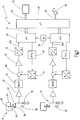
- Fig. 1 an embodiment of the new circuit arrangement is designated in its entirety by the reference numeral 10.
- the circuit arrangement 10 is shown here with a first sensor element 12 and a second sensor element 14. Each of these sensor elements has a photodiode 16 and a MOS transistor 18.
- the MOS transistor 18 has a gate 20 and two further terminals 22, 24, which are commonly referred to as source and drain. In the preferred embodiment, the gate terminal 20 and the drain terminal 24 are shorted.
- the source terminal 22 is connected to the cathode of the photodiode 16. Due to this arrangement, charge carriers, which are generated in the region of the pn junction of the photodiode 16 by impinging electromagnetic radiation 28, 30, flow through the channel 26 of the MOS transistor 18, and the MOS transistor 18 generates an output voltage whose level is logarithmic depends on the intensity of the electromagnetic radiation.
- the sensor elements 12, 14 are shown simplified here. Further advantageous details are in DE 42 09 536 A1 which discloses the basic principle of the logarithmic image cells marketed by the assignee of the present invention under the name HDRC®. In the preferred embodiments of the present invention, all sensor elements are constructed according to this HDRC® principle. In principle, however, the sensor elements can also be applied to others Be implemented manner, for example as a linear CMOS image cells or as CCD image cells.
- Fig. 1 only two sensor elements 12, 14 are shown. However, in preferred embodiments, the new circuitry 10 has a plurality of first and second sensor elements 12, 14 incorporated in FIG Fig. 1 for the sake of simplicity are not shown.
- the plurality of sensor elements 12, 14 is arranged in preferred embodiments on a semiconductor substrate, as described below with reference to FIGS Fig. 2 to 4 is explained.
- an impedance converter 32 is arranged, the output of which is connected to a multiplexer 34.
- a multiplexer 34 With the aid of the multiplexer 34, it is possible to supply a plurality of electrical signals to a common signal processing circuit.
- the in Fig. 1 1 a first multiplexer 34 is used to merge the electrical signals of the first sensor elements 12, while a second multiplexer is used to merge the electrical signals of the second sensor elements 14.
- the new circuit arrangement 10 has two parallel signal processing channels, wherein one signal processing channel processes the electrical signals of the first sensor elements 12, while the other signal processing channel processes the electrical signals of the sensor elements 14.
- the two signal processing channels have the same structure, which is why only the signal processing channel for the first sensor elements 12 is explained in more detail below.
- the output of the multiplexer 34 is connected to an adder 36.
- the adder 36 receives from a D / A converter 38, another electrical signal which is used in a conventional manner for the correction of fixed pattern noise.
- Fixed pattern noise refers to image noise that can occur in an image sensor with a large number of sensor elements, because the electrical properties of the individual sensor elements can vary due to manufacturing tolerances.
- the Fixed Pattern Noise can be corrected by adding in each case an individual correction signal to the electrical signals of the individual sensor elements.
- the correction signal is selected so that the electrical properties of the individual sensor elements are matched to one another.
- Correction coefficients for generating these correction signals are stored here in a memory 40, which is connected to a D / A converter 38.
- the D / A converter 38 uses the correction coefficients from the memory 40 to generate the correction signals for each sensor element.
- the output of the adder 36 is connected via an amplifier 42 to an A / D converter 44, which converts the corrected analog signals of the individual sensor elements into corresponding digital signals 45.
- the digital signals 45 are supplied to a microcontroller 46.
- a microcontroller it is also possible to use an ASIC, an FPGA or another signal processing circuit.
- the microcontroller 46 also serves here to write the correction coefficients for the FPN correction in the memory 40.
- the microcontroller 46 is connected here via an interface 47 to a processor 48.
- the processor 48 receives the electrical signals 45 of all first and second sensor elements 12, 14 and calculates therefrom inter alia temperature values according to the known quotient method.
- the processor 48 provides digital signals for display on a display 52.
- the screen 52 serves to display an optical image of the viewed scene in the visible wavelength range.
- the processor 48 provides signals representing the calculated temperatures.
- the output 54 may be connected to another display 56. Alternatively, the image data and temperature values may also be displayed alternately or together on the screen 52.
- the reference numeral 58 denotes a further temperature-sensitive sensor element, which is shielded in preferred embodiments against electromagnetic radiation 28, 30.
- the first and second sensor elements 12, 14 are image cells (pixels) of a matrix image sensor
- the further sensor element 58 is realized in the form of one or more diodes which are arranged in the edge region of the photosensitive surface of the sensor.
- the further sensor element 58 generates temperature information that is representative of the sensor's own temperature. This temperature information is used in preferred embodiments of the new circuitry by the controllers 46 to computationally correct the electrical signals 45 of the individual sensor elements 12, 14 such that signal variations due to temperature drift of the individual sensor elements are compensated.
- the first and second sensor elements 12, 14 are designed to receive electromagnetic radiation 28, 30 from different wavelength ranges.
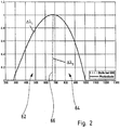
- the first sensor elements 12 are configured to receive electromagnetic radiation 28 from a first wavelength range 62 shown in the diagram in FIG Fig. 2 is shown by a solid line.
- the first wavelength range 62 includes wavelengths from about 280 nm to about 1000 nm. The maximum transmission of this first wavelength range is about 680 nm.
- Such a transmission characteristic of the first sensor elements results when the photodiodes 16 of the first sensor elements 12 are close to the surface Pn junctions are realized in a silicon semiconductor material.
- these limits are not exactly defined, but depend on the materials and process conditions used.
- the first wavelength range 62 is the wavelength range resulting from the spectral sensitivity of silicon photodiodes realized without special filters.
- the second sensor elements 14 are configured to receive electromagnetic radiation 30 from a second wavelength range 64, which is different from the first wavelength range 62.
- the second wavelength range is the "upper half" of the first wavelength range 62.
- the second wavelength range 64 results in the preferred one Embodiments in that the photodiodes of the second sensor elements 14 are provided with an additional edge filter whose transmission characteristic in Fig. 2 is shown at the dotted line 66.
- the transmission jump (cut on) is approximately 680 nm here. Electromagnetic radiation with wavelengths below 680 nm is suppressed by the edge filter. Only electromagnetic radiation with wavelengths above about 680 nm reaches the photodiodes of the second sensor elements 14.
- Fig. 3 shows a first embodiment for the realization of the sensor elements 12, 14.
- Like reference numerals denote the same elements as before.
- Fig. 3 shows a section of a semiconductor substrate 70, which is shown in cross section.
- the semiconductor substrate 70 here is a p-doped silicon substrate or a p-doped well in a semiconductor substrate.
- n-doped islands 72 are arranged in the p-doped substrate 70 .
- another p-doped layer 74 is disposed in the p-doped substrate 70 .
- the pn junction 76 forms the photodiode 16 of the first sensor element 12, while the pn junction 78 forms the photodiode 16 of the second sensor element 14.
- the longer wavelength radiation 30 penetrates deeper into the semiconductor material and thus reaches the deeper pn junction 78, while the shorter wavelength radiation 28 only reaches the upper pn junction 76.
- the layers of the upper pn junction 76 form a filter for the lower pn junction 78.
- the position of the pn junctions 76, 78 is chosen here as a function of the penetration depth of the radiation to be detected.
- a plurality of such stacked photodiodes are arranged side by side in the semiconductor substrate 70.
- the sensor elements 12, 14 together form the individual pixels of the matrix sensor. It is understood that each pixel also includes the MOS transistors and, in preferred embodiments, other devices such as the impedance converter 32. These further components are not shown here for the sake of simplicity.
- Fig. 4 shows a further embodiment, as stacked first and second sensor elements 12, 14 can be realized.
- the sensor elements 12, 14 are realized on an n-doped substrate 70 'by way of example.
- a plurality of self-conductive layers 80 are disposed, over which p-doped layers 82 are located.
- a multiplicity of pin diodes 84 are formed which serve as photodiodes for the second sensor elements 14.
- a continuous insulating layer 85 of silicon dioxide is arranged over the pin diodes 84.
- a plurality of further pin diodes with a layer sequence of n-doped silicon 86, self-conducting silicon 88 and p-doped silicon 90 is arranged on the insulation layer 85.
- the pin diodes with the layer sequence 86, 88, 90 form the first sensor elements 12.
- the layers 86, 88, 90 are produced by means of a CVD method.
- a realization according to the embodiment in Fig. 4 has the advantage that the photodiodes of the sensor elements 12, 14 are stacked on top of each other, but are electrically separated from each other by the insulating layer 85.
- the photodiodes of the two sensor elements 12, 14 are potential-free through the insulation and can therefore be interconnected as desired.
- the islands 72 in the embodiment form according to FIG Fig. 3 a common cathode terminal of the two photodiodes for the sensor elements 12, 14th
- Fig. 5 shows a further embodiment in which the photodiodes of the sensor elements 12, 14 are not arranged vertically one above the other, but horizontally next to each other.
- the photodiodes of the sensor elements 12, 14 are constructed substantially identical.
- these are again pin photodiodes with layers 80, 82 which are arranged in an n-doped silicon substrate 70 "In order to achieve the different spectral sensitivities, a filter 92 is provided above the photodiodes for the second sensor elements 14 arranged, the filter characteristic of the dotted line 66 from Fig. 2 equivalent.
- the filter 92 is implemented as a dielectric interference filter and has an upper layer 94 of silicon nitride, a middle layer 96 of silicon, and a lower layer 98 of silicon nitride.
- the Layers 94 to 98 can in turn be produced by means of a CVD method.
- the sensor elements 12, 14 may be alternately arranged on the surface of the semiconductor substrate 70 'in the manner of a checkerboard pattern or line by line or in columns. Compared to a sensor according to the embodiments according to 3 or 4 the resolution is lower. Each sensor element 12, 14 here forms a separate pixel of the matrix sensor. On the other hand, the sensor elements 12, 14 can be produced here in common process steps. At the end of the process sequence, it is sufficient if the photodiodes of the second sensor elements 14 are covered with the layers 94 to 98.
Landscapes
- Physics & Mathematics (AREA)
- General Physics & Mathematics (AREA)
- Spectroscopy & Molecular Physics (AREA)
- Solid State Image Pick-Up Elements (AREA)
- Radiation Pyrometers (AREA)
Claims (8)
- Arrangement de circuit destiné à générer des signaux (45) dépendant de la lumière et de la température, lesquels représentent les propriétés d'une scène, comprenant des éléments de détection (12, 14) qui génèrent une pluralité de premiers et de deuxièmes signaux électriques (45a, 45b) en fonction d'un rayonnement électromagnétique (28, 30) incident, les premiers signaux électriques (45a) étant générés en fonction du rayonnement électromagnétique (28) issu d'une première plage de longueurs d'onde (62), laquelle contient au moins une grande partie de la lumière visible, et les deuxièmes signaux électriques (45b) étant générés en fonction du rayonnement électromagnétique (30) issu d'une deuxième plage de longueurs d'onde (64), laquelle contient principalement un rayonnement infrarouge, la première plage de longueurs d'onde (62) chevauchant la deuxième plage de longueurs d'onde (64) et contenant ainsi également un rayonnement infrarouge, caractérisé en ce que les éléments de détection contiennent une pluralité de premiers (12) et de deuxièmes (14) éléments de détection, les premiers et deuxièmes éléments de détection (12, 14) étant deux types différents d'éléments de détection qui sont configurés pour capter un rayonnement électromagnétique (28, 30) issu de plages de longueurs d'onde différentes, la première plage de longueurs d'onde (62) chevauchant largement entièrement la deuxième plage de longueurs d'onde (64),
le deuxième élément de détection (14) comportant un filtre à arêtes (92) qui définit une limite inférieure (66) de la deuxième plage de longueurs d'onde (64), et la limite inférieure (66) se trouvant sensiblement au centre par rapport à la première plage de longueurs d'onde (62). - Arrangement de circuit selon la revendication 1, caractérisé par une partie de circuit (48) qui est configurée pour déterminer une température de la scène en fonction des premiers et des deuxièmes signaux (45a, 45b).
- Arrangement de circuit selon la revendication 1 ou 2, caractérisé par un substrat en semiconducteur (70) sur lequel sont disposés les uns à côté des autres une pluralité de premiers et deuxièmes éléments de détection (12, 14).
- Arrangement de circuit selon l'une des revendications 1 à 3, caractérisé en ce que les premiers et deuxièmes éléments de détection (12, 14) sont respectivement disposés les uns au-dessus des autres.
- Arrangement de circuit selon l'une des revendications 1 à 4, caractérisé en ce que les premiers et deuxièmes éléments de détection (12, 14) comportent respectivement une photodiode (16) et au moins un transistor MOS (18) doté d'une borne de gâchette (20), de deux bornes (22, 24) supplémentaires et d'un canal (26), la photodiode (16) étant connectée au transistor MOS (18) de telle sorte que les porteurs de charge générés dans la photodiode (16) s'échappent à travers le canal (26) et la borne de gâchette (20) étant reliée de manière conductrice avec l'une des deux bornes (24) supplémentaires.
- Arrangement de circuit selon l'une des revendications 1 à 5, caractérisé en ce que le filtre à arêtes (92) est un filtre à interférence diélectrique comprenant une pluralité de couches de matière (94-98) disposées les unes au-dessus des autres, les couches de matière (94-98) étant pour l'essentiel constituées de silicium et de nitrure de silicium.
- Arrangement de circuit selon l'une des revendications 1 à 6, caractérisé par au moins un élément de détection (58) sensible à la température supplémentaire qui est protégé par blindage contre le rayonnement électromagnétique issu de la première et de la deuxième plage de longueurs d'onde (62, 64).
- Utilisation d'un arrangement de circuit selon l'une des revendications 1 à 7 en tant que pyromètre, notamment en tant que pyromètre d'imagerie.
Applications Claiming Priority (2)
| Application Number | Priority Date | Filing Date | Title |
|---|---|---|---|
| DE102007054314A DE102007054314A1 (de) | 2007-11-05 | 2007-11-05 | Schaltungsanordnung zum Erzeugen von licht- und temperaturabhängigen Signalen, insbesondere für ein bildgebendes Pyrometer |
| PCT/EP2008/009167 WO2009059721A1 (fr) | 2007-11-05 | 2008-10-30 | Circuiterie pour la production de signaux dépendant de la luminosité et de la température, notamment pour un pyromètre produisant des images |
Publications (2)
| Publication Number | Publication Date |
|---|---|
| EP2210073A1 EP2210073A1 (fr) | 2010-07-28 |
| EP2210073B1 true EP2210073B1 (fr) | 2017-05-17 |
Family
ID=40262259
Family Applications (1)
| Application Number | Title | Priority Date | Filing Date |
|---|---|---|---|
| EP08846593.5A Active EP2210073B1 (fr) | 2007-11-05 | 2008-10-30 | Circuiterie pour la production de signaux dépendant de la luminosité et de la température, notamment pour un pyromètre produisant des images |
Country Status (7)
| Country | Link |
|---|---|
| US (1) | US8309924B2 (fr) |
| EP (1) | EP2210073B1 (fr) |
| JP (1) | JP2011503560A (fr) |
| KR (1) | KR20100084565A (fr) |
| CN (1) | CN101910809A (fr) |
| DE (1) | DE102007054314A1 (fr) |
| WO (1) | WO2009059721A1 (fr) |
Families Citing this family (9)
| Publication number | Priority date | Publication date | Assignee | Title |
|---|---|---|---|---|
| JP5768477B2 (ja) * | 2011-05-02 | 2015-08-26 | 新日鐵住金株式会社 | 被加工材の温度測定方法、加工品の製造方法、及び被加工材の加熱装置 |
| DE102012112412A1 (de) * | 2012-12-17 | 2014-06-18 | LumaSense Technologies GmbH | Vorrichtung und Verfahren zur Messung einer ortsaufgelösten Temperaturverteilung |
| CN106796861B (zh) * | 2014-04-17 | 2019-05-03 | 加坦公司 | 混合能量转换与处理检测器 |
| US9899550B2 (en) | 2015-08-12 | 2018-02-20 | Toyota Motor Engineering & Manufacturing North America, Inc. | Electric power transfer system using optical power transfer |
| FR3067167B1 (fr) * | 2017-06-06 | 2019-06-28 | Office National D'etudes Et De Recherches Aerospatiales | Element de conversion spectrale pour rayonnement electromagnetique |
| US11644365B2 (en) | 2017-10-03 | 2023-05-09 | Philip Morris Products S.A. | Aerosol-generating device and system comprising a pyrometer |
| DE102018133518B4 (de) | 2018-12-21 | 2023-07-06 | Bias Bremer Institut Für Angewandte Strahltechnik | Kamera zum Bestimmen eines 2D-Wärmebilds sowie System und Prozessregeleinrichtung |
| CN113049589B (zh) * | 2021-03-10 | 2021-12-03 | 清华大学 | 高温环境下可调控的图像获取方法 |
| CA3252665A1 (fr) * | 2022-05-27 | 2023-11-30 | Basf Corporation | Conception de circuits électroniques de pyromètre pour protocoles industriels modernes |
Family Cites Families (19)
| Publication number | Priority date | Publication date | Assignee | Title |
|---|---|---|---|---|
| DE867453C (de) | 1942-12-13 | 1953-02-16 | Siemens Ag | Verfahren zur selbsttaetigen Messung der Farbtemperatur mittels lichtelektrischer Zellen |
| DE1237804B (de) | 1958-04-01 | 1967-03-30 | Shaw Instr Corp | Farbpyrometer |
| DE1136135B (de) | 1960-08-29 | 1962-09-06 | Siemens Ag | Farbpyrometer mit zwei flaechenhaften Strahlungsempfaengern |
| US3435237A (en) * | 1965-01-21 | 1969-03-25 | Prd Electronics Inc | Radiation discriminator means |
| US3535237A (en) * | 1967-04-25 | 1970-10-20 | Texaco Inc | Drilling fluid |
| GB1507367A (en) | 1974-06-10 | 1978-04-12 | Siemens Ag | Automatic radiation pyrometer |
| US4413324A (en) | 1981-02-25 | 1983-11-01 | Sumitomo Kinzoku Kogyo Kabushiki Kaisha | Temperature pattern measuring method and a device therefor |
| US4570332A (en) | 1982-05-10 | 1986-02-18 | Sharp Kabushiki Kaisha | Method of forming contact to thin film semiconductor device |
| EP0129150B1 (fr) * | 1983-06-16 | 1989-04-26 | Deutsche Forschungsanstalt für Luft- und Raumfahrt e.V. | Procédé pour mesurer sans contact et indépendemment du pouvoir émissif la température d'un objet par mesure du rayonnement, et dispositif pour la mise en oeuvre du procédé |
| US4681434A (en) * | 1985-11-14 | 1987-07-21 | United Technologies Corporation | Dual spectra optical pyrometer having a serial array of photodectectors |
| DE4209536C3 (de) | 1992-03-24 | 2000-10-05 | Stuttgart Mikroelektronik | Bildzelle für einen Bildaufnehmer-Chip |
| JP2856180B2 (ja) * | 1996-11-27 | 1999-02-10 | 日本電気株式会社 | 熱型赤外線検出素子とその製造方法 |
| DE19650705A1 (de) | 1996-12-08 | 1998-06-10 | Robert Prof Dr Ing Massen | Multisensorielle Kamera mit kompakter Sensoranordnung |
| US5963311A (en) * | 1997-09-12 | 1999-10-05 | Stratonics, Inc. | Surface and particle imaging pyrometer and method of use |
| DE60012474T2 (de) | 2000-03-13 | 2004-11-25 | Csem Centre Suisse D'electronique Et De Microtechnique S.A. | Bildgebendes pyrometer |
| JP4578797B2 (ja) * | 2003-11-10 | 2010-11-10 | パナソニック株式会社 | 撮像装置 |
| AT501638A1 (de) * | 2005-04-13 | 2006-10-15 | Ruebig Gmbh & Co Kg | Vorrichtung zum berührungslosen temperaturmessen |
| US20070145273A1 (en) * | 2005-12-22 | 2007-06-28 | Chang Edward T | High-sensitivity infrared color camera |
| KR100863497B1 (ko) * | 2007-06-19 | 2008-10-14 | 마루엘에스아이 주식회사 | 이미지 감지 장치, 이미지 신호 처리 방법, 광 감지 소자, 제어 방법 및 화소 어레이 |
-
2007
- 2007-11-05 DE DE102007054314A patent/DE102007054314A1/de not_active Withdrawn
-
2008
- 2008-10-30 CN CN2008801239578A patent/CN101910809A/zh active Pending
- 2008-10-30 JP JP2010532478A patent/JP2011503560A/ja active Pending
- 2008-10-30 KR KR1020107011629A patent/KR20100084565A/ko not_active Withdrawn
- 2008-10-30 WO PCT/EP2008/009167 patent/WO2009059721A1/fr not_active Ceased
- 2008-10-30 EP EP08846593.5A patent/EP2210073B1/fr active Active
-
2010
- 2010-05-04 US US12/773,349 patent/US8309924B2/en not_active Expired - Fee Related
Also Published As
| Publication number | Publication date |
|---|---|
| US20100278212A1 (en) | 2010-11-04 |
| US8309924B2 (en) | 2012-11-13 |
| CN101910809A (zh) | 2010-12-08 |
| EP2210073A1 (fr) | 2010-07-28 |
| WO2009059721A1 (fr) | 2009-05-14 |
| JP2011503560A (ja) | 2011-01-27 |
| DE102007054314A1 (de) | 2009-05-07 |
| KR20100084565A (ko) | 2010-07-26 |
Similar Documents
| Publication | Publication Date | Title |
|---|---|---|
| EP2210073B1 (fr) | Circuiterie pour la production de signaux dépendant de la luminosité et de la température, notamment pour un pyromètre produisant des images | |
| DE60035580T2 (de) | Halbleiter | |
| DE69317752T2 (de) | Festkörpers-Bildaufnahmeeinrichtung | |
| DE60031590T2 (de) | Bildsensor | |
| DE3486284T2 (de) | Sichtbarmachungs/Infrarot-Bildgerät mit einer Stapelzellenstruktur. | |
| DE69729648T2 (de) | Aktivpixelsensormatrix mit mehrfachauflösungsausgabe | |
| DE68917242T2 (de) | Festkörperbildsensor. | |
| DE69528386T2 (de) | Abbildungssystem | |
| DE69325182T2 (de) | Festkörper-Bildaufnahmevorrichtung | |
| DE202017102626U1 (de) | Doppel-Photodioden-Bildpixel | |
| DE112019003270B4 (de) | Umgebungslichtsensor | |
| DE19857851A1 (de) | Detektionsgerät für physikalische und/oder chemische Größen | |
| DE2741226B2 (de) | Festkörper-Farbbildaufnahmeeinrichtung | |
| DE10153378A1 (de) | Photosensoranordnung mit gemeinsamen Strukturen | |
| EP0343366A1 (fr) | Caméra | |
| DE102011053219A1 (de) | Kombiniertes Pixel mit phasensensitivem und farbselektivem Subpixel | |
| DE112021004358T5 (de) | Festkörperbildgebungsvorrichtung und elektronische vorrichtung | |
| DE112021000990T5 (de) | Verbesserungen für spad-basierte fotodetektoren | |
| DE102005005590A1 (de) | Lichtfilternder Bildsensor | |
| DE69223841T2 (de) | Bilderempfangsapparat | |
| DE112021003978T5 (de) | Abbildungsvorrichtung | |
| DE102020209822A1 (de) | Sensor und verfahren zum bilden von selbigem | |
| EP4014027B1 (fr) | Procédé et dispositif d'analyse d'une cellule solaire multijonction dotée d'au moins deux sous-cellules solaires au moyen d'un rayonnement luminescent | |
| DE112014000624T5 (de) | Fotodioden-Anordnung mit einer ladungsabsorbierenden dotierten Zone | |
| DE69222230T2 (de) | Festkörper-Bildaufnahmevorrichtung |
Legal Events
| Date | Code | Title | Description |
|---|---|---|---|
| PUAI | Public reference made under article 153(3) epc to a published international application that has entered the european phase |
Free format text: ORIGINAL CODE: 0009012 |
|
| 17P | Request for examination filed |
Effective date: 20100602 |
|
| AK | Designated contracting states |
Kind code of ref document: A1 Designated state(s): AT BE BG CH CY CZ DE DK EE ES FI FR GB GR HR HU IE IS IT LI LT LU LV MC MT NL NO PL PT RO SE SI SK TR |
|
| AX | Request for extension of the european patent |
Extension state: AL BA MK RS |
|
| DAX | Request for extension of the european patent (deleted) | ||
| 17Q | First examination report despatched |
Effective date: 20160513 |
|
| GRAP | Despatch of communication of intention to grant a patent |
Free format text: ORIGINAL CODE: EPIDOSNIGR1 |
|
| GRAJ | Information related to disapproval of communication of intention to grant by the applicant or resumption of examination proceedings by the epo deleted |
Free format text: ORIGINAL CODE: EPIDOSDIGR1 |
|
| GRAP | Despatch of communication of intention to grant a patent |
Free format text: ORIGINAL CODE: EPIDOSNIGR1 |
|
| INTG | Intention to grant announced |
Effective date: 20161123 |
|
| INTC | Intention to grant announced (deleted) | ||
| INTG | Intention to grant announced |
Effective date: 20161220 |
|
| GRAS | Grant fee paid |
Free format text: ORIGINAL CODE: EPIDOSNIGR3 |
|
| GRAA | (expected) grant |
Free format text: ORIGINAL CODE: 0009210 |
|
| AK | Designated contracting states |
Kind code of ref document: B1 Designated state(s): AT BE BG CH CY CZ DE DK EE ES FI FR GB GR HR HU IE IS IT LI LT LU LV MC MT NL NO PL PT RO SE SI SK TR |
|
| REG | Reference to a national code |
Ref country code: GB Ref legal event code: FG4D Free format text: NOT ENGLISH |
|
| REG | Reference to a national code |
Ref country code: CH Ref legal event code: EP |
|
| REG | Reference to a national code |
Ref country code: IE Ref legal event code: FG4D Free format text: LANGUAGE OF EP DOCUMENT: GERMAN |
|
| REG | Reference to a national code |
Ref country code: AT Ref legal event code: REF Ref document number: 894887 Country of ref document: AT Kind code of ref document: T Effective date: 20170615 |
|
| REG | Reference to a national code |
Ref country code: DE Ref legal event code: R096 Ref document number: 502008015318 Country of ref document: DE |
|
| REG | Reference to a national code |
Ref country code: NL Ref legal event code: MP Effective date: 20170517 |
|
| REG | Reference to a national code |
Ref country code: LT Ref legal event code: MG4D |
|
| REG | Reference to a national code |
Ref country code: FR Ref legal event code: PLFP Year of fee payment: 10 |
|
| PG25 | Lapsed in a contracting state [announced via postgrant information from national office to epo] |
Ref country code: ES Free format text: LAPSE BECAUSE OF FAILURE TO SUBMIT A TRANSLATION OF THE DESCRIPTION OR TO PAY THE FEE WITHIN THE PRESCRIBED TIME-LIMIT Effective date: 20170517 Ref country code: NO Free format text: LAPSE BECAUSE OF FAILURE TO SUBMIT A TRANSLATION OF THE DESCRIPTION OR TO PAY THE FEE WITHIN THE PRESCRIBED TIME-LIMIT Effective date: 20170817 Ref country code: LT Free format text: LAPSE BECAUSE OF FAILURE TO SUBMIT A TRANSLATION OF THE DESCRIPTION OR TO PAY THE FEE WITHIN THE PRESCRIBED TIME-LIMIT Effective date: 20170517 Ref country code: HR Free format text: LAPSE BECAUSE OF FAILURE TO SUBMIT A TRANSLATION OF THE DESCRIPTION OR TO PAY THE FEE WITHIN THE PRESCRIBED TIME-LIMIT Effective date: 20170517 Ref country code: FI Free format text: LAPSE BECAUSE OF FAILURE TO SUBMIT A TRANSLATION OF THE DESCRIPTION OR TO PAY THE FEE WITHIN THE PRESCRIBED TIME-LIMIT Effective date: 20170517 Ref country code: GR Free format text: LAPSE BECAUSE OF FAILURE TO SUBMIT A TRANSLATION OF THE DESCRIPTION OR TO PAY THE FEE WITHIN THE PRESCRIBED TIME-LIMIT Effective date: 20170818 |
|
| PG25 | Lapsed in a contracting state [announced via postgrant information from national office to epo] |
Ref country code: BG Free format text: LAPSE BECAUSE OF FAILURE TO SUBMIT A TRANSLATION OF THE DESCRIPTION OR TO PAY THE FEE WITHIN THE PRESCRIBED TIME-LIMIT Effective date: 20170817 Ref country code: SE Free format text: LAPSE BECAUSE OF FAILURE TO SUBMIT A TRANSLATION OF THE DESCRIPTION OR TO PAY THE FEE WITHIN THE PRESCRIBED TIME-LIMIT Effective date: 20170517 Ref country code: IS Free format text: LAPSE BECAUSE OF FAILURE TO SUBMIT A TRANSLATION OF THE DESCRIPTION OR TO PAY THE FEE WITHIN THE PRESCRIBED TIME-LIMIT Effective date: 20170917 Ref country code: LV Free format text: LAPSE BECAUSE OF FAILURE TO SUBMIT A TRANSLATION OF THE DESCRIPTION OR TO PAY THE FEE WITHIN THE PRESCRIBED TIME-LIMIT Effective date: 20170517 Ref country code: PL Free format text: LAPSE BECAUSE OF FAILURE TO SUBMIT A TRANSLATION OF THE DESCRIPTION OR TO PAY THE FEE WITHIN THE PRESCRIBED TIME-LIMIT Effective date: 20170517 Ref country code: NL Free format text: LAPSE BECAUSE OF FAILURE TO SUBMIT A TRANSLATION OF THE DESCRIPTION OR TO PAY THE FEE WITHIN THE PRESCRIBED TIME-LIMIT Effective date: 20170517 |
|
| PG25 | Lapsed in a contracting state [announced via postgrant information from national office to epo] |
Ref country code: CZ Free format text: LAPSE BECAUSE OF FAILURE TO SUBMIT A TRANSLATION OF THE DESCRIPTION OR TO PAY THE FEE WITHIN THE PRESCRIBED TIME-LIMIT Effective date: 20170517 Ref country code: DK Free format text: LAPSE BECAUSE OF FAILURE TO SUBMIT A TRANSLATION OF THE DESCRIPTION OR TO PAY THE FEE WITHIN THE PRESCRIBED TIME-LIMIT Effective date: 20170517 Ref country code: SK Free format text: LAPSE BECAUSE OF FAILURE TO SUBMIT A TRANSLATION OF THE DESCRIPTION OR TO PAY THE FEE WITHIN THE PRESCRIBED TIME-LIMIT Effective date: 20170517 Ref country code: EE Free format text: LAPSE BECAUSE OF FAILURE TO SUBMIT A TRANSLATION OF THE DESCRIPTION OR TO PAY THE FEE WITHIN THE PRESCRIBED TIME-LIMIT Effective date: 20170517 Ref country code: RO Free format text: LAPSE BECAUSE OF FAILURE TO SUBMIT A TRANSLATION OF THE DESCRIPTION OR TO PAY THE FEE WITHIN THE PRESCRIBED TIME-LIMIT Effective date: 20170517 |
|
| REG | Reference to a national code |
Ref country code: DE Ref legal event code: R097 Ref document number: 502008015318 Country of ref document: DE |
|
| PG25 | Lapsed in a contracting state [announced via postgrant information from national office to epo] |
Ref country code: IT Free format text: LAPSE BECAUSE OF FAILURE TO SUBMIT A TRANSLATION OF THE DESCRIPTION OR TO PAY THE FEE WITHIN THE PRESCRIBED TIME-LIMIT Effective date: 20170517 |
|
| PLBE | No opposition filed within time limit |
Free format text: ORIGINAL CODE: 0009261 |
|
| STAA | Information on the status of an ep patent application or granted ep patent |
Free format text: STATUS: NO OPPOSITION FILED WITHIN TIME LIMIT |
|
| 26N | No opposition filed |
Effective date: 20180220 |
|
| PG25 | Lapsed in a contracting state [announced via postgrant information from national office to epo] |
Ref country code: SI Free format text: LAPSE BECAUSE OF FAILURE TO SUBMIT A TRANSLATION OF THE DESCRIPTION OR TO PAY THE FEE WITHIN THE PRESCRIBED TIME-LIMIT Effective date: 20170517 Ref country code: MC Free format text: LAPSE BECAUSE OF FAILURE TO SUBMIT A TRANSLATION OF THE DESCRIPTION OR TO PAY THE FEE WITHIN THE PRESCRIBED TIME-LIMIT Effective date: 20170517 |
|
| REG | Reference to a national code |
Ref country code: CH Ref legal event code: PL |
|
| REG | Reference to a national code |
Ref country code: IE Ref legal event code: MM4A |
|
| PG25 | Lapsed in a contracting state [announced via postgrant information from national office to epo] |
Ref country code: CH Free format text: LAPSE BECAUSE OF NON-PAYMENT OF DUE FEES Effective date: 20171031 Ref country code: LU Free format text: LAPSE BECAUSE OF NON-PAYMENT OF DUE FEES Effective date: 20171030 Ref country code: LI Free format text: LAPSE BECAUSE OF NON-PAYMENT OF DUE FEES Effective date: 20171031 |
|
| REG | Reference to a national code |
Ref country code: BE Ref legal event code: MM Effective date: 20171031 |
|
| PG25 | Lapsed in a contracting state [announced via postgrant information from national office to epo] |
Ref country code: BE Free format text: LAPSE BECAUSE OF NON-PAYMENT OF DUE FEES Effective date: 20171031 |
|
| PG25 | Lapsed in a contracting state [announced via postgrant information from national office to epo] |
Ref country code: MT Free format text: LAPSE BECAUSE OF FAILURE TO SUBMIT A TRANSLATION OF THE DESCRIPTION OR TO PAY THE FEE WITHIN THE PRESCRIBED TIME-LIMIT Effective date: 20170517 |
|
| REG | Reference to a national code |
Ref country code: FR Ref legal event code: PLFP Year of fee payment: 11 |
|
| PG25 | Lapsed in a contracting state [announced via postgrant information from national office to epo] |
Ref country code: IE Free format text: LAPSE BECAUSE OF NON-PAYMENT OF DUE FEES Effective date: 20171030 |
|
| REG | Reference to a national code |
Ref country code: AT Ref legal event code: MM01 Ref document number: 894887 Country of ref document: AT Kind code of ref document: T Effective date: 20171030 |
|
| PG25 | Lapsed in a contracting state [announced via postgrant information from national office to epo] |
Ref country code: AT Free format text: LAPSE BECAUSE OF NON-PAYMENT OF DUE FEES Effective date: 20171030 |
|
| PG25 | Lapsed in a contracting state [announced via postgrant information from national office to epo] |
Ref country code: HU Free format text: LAPSE BECAUSE OF FAILURE TO SUBMIT A TRANSLATION OF THE DESCRIPTION OR TO PAY THE FEE WITHIN THE PRESCRIBED TIME-LIMIT; INVALID AB INITIO Effective date: 20081030 |
|
| PG25 | Lapsed in a contracting state [announced via postgrant information from national office to epo] |
Ref country code: CY Free format text: LAPSE BECAUSE OF NON-PAYMENT OF DUE FEES Effective date: 20170517 |
|
| PG25 | Lapsed in a contracting state [announced via postgrant information from national office to epo] |
Ref country code: TR Free format text: LAPSE BECAUSE OF FAILURE TO SUBMIT A TRANSLATION OF THE DESCRIPTION OR TO PAY THE FEE WITHIN THE PRESCRIBED TIME-LIMIT Effective date: 20170517 |
|
| PG25 | Lapsed in a contracting state [announced via postgrant information from national office to epo] |
Ref country code: PT Free format text: LAPSE BECAUSE OF FAILURE TO SUBMIT A TRANSLATION OF THE DESCRIPTION OR TO PAY THE FEE WITHIN THE PRESCRIBED TIME-LIMIT Effective date: 20170517 |
|
| PGFP | Annual fee paid to national office [announced via postgrant information from national office to epo] |
Ref country code: GB Payment date: 20201022 Year of fee payment: 13 |
|
| GBPC | Gb: european patent ceased through non-payment of renewal fee |
Effective date: 20211030 |
|
| PG25 | Lapsed in a contracting state [announced via postgrant information from national office to epo] |
Ref country code: GB Free format text: LAPSE BECAUSE OF NON-PAYMENT OF DUE FEES Effective date: 20211030 |
|
| PGFP | Annual fee paid to national office [announced via postgrant information from national office to epo] |
Ref country code: DE Payment date: 20251028 Year of fee payment: 18 |
|
| PGFP | Annual fee paid to national office [announced via postgrant information from national office to epo] |
Ref country code: FR Payment date: 20251029 Year of fee payment: 18 |