EP2214042B1 - Procédé de production d'un dispositif photonique et dispositif photonique correspondant - Google Patents
Procédé de production d'un dispositif photonique et dispositif photonique correspondant Download PDFInfo
- Publication number
- EP2214042B1 EP2214042B1 EP09290077.8A EP09290077A EP2214042B1 EP 2214042 B1 EP2214042 B1 EP 2214042B1 EP 09290077 A EP09290077 A EP 09290077A EP 2214042 B1 EP2214042 B1 EP 2214042B1
- Authority
- EP
- European Patent Office
- Prior art keywords
- layer
- photodetector
- light source
- contact layer
- waveguide
- Prior art date
- Legal status (The legal status is an assumption and is not a legal conclusion. Google has not performed a legal analysis and makes no representation as to the accuracy of the status listed.)
- Not-in-force
Links
- 238000000034 method Methods 0.000 title claims description 37
- 239000000758 substrate Substances 0.000 claims description 26
- 238000005530 etching Methods 0.000 claims description 16
- 239000000463 material Substances 0.000 claims description 9
- 230000008021 deposition Effects 0.000 claims description 7
- FGUUSXIOTUKUDN-IBGZPJMESA-N C1(=CC=CC=C1)N1C2=C(NC([C@H](C1)NC=1OC(=NN=1)C1=CC=CC=C1)=O)C=CC=C2 Chemical compound C1(=CC=CC=C1)N1C2=C(NC([C@H](C1)NC=1OC(=NN=1)C1=CC=CC=C1)=O)C=CC=C2 FGUUSXIOTUKUDN-IBGZPJMESA-N 0.000 claims description 2
- 239000004020 conductor Substances 0.000 claims description 2
- 229910052710 silicon Inorganic materials 0.000 description 23
- 239000010703 silicon Substances 0.000 description 23
- XUIMIQQOPSSXEZ-UHFFFAOYSA-N Silicon Chemical compound [Si] XUIMIQQOPSSXEZ-UHFFFAOYSA-N 0.000 description 21
- 230000008569 process Effects 0.000 description 17
- 230000008878 coupling Effects 0.000 description 11
- 238000010168 coupling process Methods 0.000 description 11
- 238000005859 coupling reaction Methods 0.000 description 11
- 230000000694 effects Effects 0.000 description 10
- VYPSYNLAJGMNEJ-UHFFFAOYSA-N silicon dioxide Inorganic materials O=[Si]=O VYPSYNLAJGMNEJ-UHFFFAOYSA-N 0.000 description 8
- 238000010521 absorption reaction Methods 0.000 description 7
- 238000000151 deposition Methods 0.000 description 6
- 238000000407 epitaxy Methods 0.000 description 5
- 239000000203 mixture Substances 0.000 description 5
- 229910000530 Gallium indium arsenide Inorganic materials 0.000 description 4
- 238000013459 approach Methods 0.000 description 4
- 238000000206 photolithography Methods 0.000 description 4
- 229910052681 coesite Inorganic materials 0.000 description 3
- 229910052906 cristobalite Inorganic materials 0.000 description 3
- 238000001514 detection method Methods 0.000 description 3
- 230000005672 electromagnetic field Effects 0.000 description 3
- 238000005516 engineering process Methods 0.000 description 3
- 239000012212 insulator Substances 0.000 description 3
- 238000001459 lithography Methods 0.000 description 3
- 230000003287 optical effect Effects 0.000 description 3
- 238000001020 plasma etching Methods 0.000 description 3
- 229910052682 stishovite Inorganic materials 0.000 description 3
- 229910052905 tridymite Inorganic materials 0.000 description 3
- 238000001312 dry etching Methods 0.000 description 2
- 230000010354 integration Effects 0.000 description 2
- 238000002488 metal-organic chemical vapour deposition Methods 0.000 description 2
- 238000001451 molecular beam epitaxy Methods 0.000 description 2
- 238000012544 monitoring process Methods 0.000 description 2
- 229920002120 photoresistant polymer Polymers 0.000 description 2
- 238000012545 processing Methods 0.000 description 2
- 235000012239 silicon dioxide Nutrition 0.000 description 2
- 239000000377 silicon dioxide Substances 0.000 description 2
- 229910052814 silicon oxide Inorganic materials 0.000 description 2
- 238000001039 wet etching Methods 0.000 description 2
- 229910001218 Gallium arsenide Inorganic materials 0.000 description 1
- QAOWNCQODCNURD-UHFFFAOYSA-N Sulfuric acid Chemical compound OS(O)(=O)=O QAOWNCQODCNURD-UHFFFAOYSA-N 0.000 description 1
- 239000011149 active material Substances 0.000 description 1
- 229910045601 alloy Inorganic materials 0.000 description 1
- 239000000956 alloy Substances 0.000 description 1
- 229910021417 amorphous silicon Inorganic materials 0.000 description 1
- 230000008901 benefit Effects 0.000 description 1
- 238000003486 chemical etching Methods 0.000 description 1
- 230000000295 complement effect Effects 0.000 description 1
- 150000001875 compounds Chemical class 0.000 description 1
- 229910021419 crystalline silicon Inorganic materials 0.000 description 1
- 230000007423 decrease Effects 0.000 description 1
- 238000013461 design Methods 0.000 description 1
- 239000003989 dielectric material Substances 0.000 description 1
- 238000009826 distribution Methods 0.000 description 1
- 229910044991 metal oxide Inorganic materials 0.000 description 1
- 150000004706 metal oxides Chemical class 0.000 description 1
- 238000001465 metallisation Methods 0.000 description 1
- 238000013041 optical simulation Methods 0.000 description 1
- 238000005457 optimization Methods 0.000 description 1
- 238000005498 polishing Methods 0.000 description 1
- 239000002096 quantum dot Substances 0.000 description 1
- 238000011160 research Methods 0.000 description 1
- 239000004065 semiconductor Substances 0.000 description 1
- 238000004088 simulation Methods 0.000 description 1
- 230000007480 spreading Effects 0.000 description 1
- 238000003892 spreading Methods 0.000 description 1
- 239000000126 substance Substances 0.000 description 1
- 235000011149 sulphuric acid Nutrition 0.000 description 1
- 239000010409 thin film Substances 0.000 description 1
Images
Classifications
-
- G—PHYSICS
- G02—OPTICS
- G02B—OPTICAL ELEMENTS, SYSTEMS OR APPARATUS
- G02B6/00—Light guides; Structural details of arrangements comprising light guides and other optical elements, e.g. couplings
- G02B6/24—Coupling light guides
- G02B6/42—Coupling light guides with opto-electronic elements
- G02B6/43—Arrangements comprising a plurality of opto-electronic elements and associated optical interconnections
-
- G—PHYSICS
- G02—OPTICS
- G02B—OPTICAL ELEMENTS, SYSTEMS OR APPARATUS
- G02B6/00—Light guides; Structural details of arrangements comprising light guides and other optical elements, e.g. couplings
- G02B6/10—Light guides; Structural details of arrangements comprising light guides and other optical elements, e.g. couplings of the optical waveguide type
- G02B6/12—Light guides; Structural details of arrangements comprising light guides and other optical elements, e.g. couplings of the optical waveguide type of the integrated circuit kind
- G02B6/13—Integrated optical circuits characterised by the manufacturing method
-
- G—PHYSICS
- G02—OPTICS
- G02B—OPTICAL ELEMENTS, SYSTEMS OR APPARATUS
- G02B6/00—Light guides; Structural details of arrangements comprising light guides and other optical elements, e.g. couplings
- G02B6/10—Light guides; Structural details of arrangements comprising light guides and other optical elements, e.g. couplings of the optical waveguide type
- G02B6/12—Light guides; Structural details of arrangements comprising light guides and other optical elements, e.g. couplings of the optical waveguide type of the integrated circuit kind
- G02B6/13—Integrated optical circuits characterised by the manufacturing method
- G02B6/136—Integrated optical circuits characterised by the manufacturing method by etching
Definitions
- This invention is related to the field of silicon photonics.
- CMOS silicon wafer Complementary Metal Oxide Semiconductor silicon wafer.
- PIC Photonic Integrated Circuit
- silicon into Si02
- CMOS layer CMOS layer
- telecom wavelength comprised between 1,3 and 1,55 ⁇ m.
- silicon has a very poor photon emission efficiency.
- III-V materials known to have very good photon emission and detection efficiencies, on top of the CMOS layers, by means of die to wafer bonding on silicon wafer.
- a reference can be found in G. Roelkens et al., III-V/ Si photonics by die-to-wafer bonding, Materials Todays 2007, vol.10, n° 7-8, pp. 36-43 .
- a typical structure includes a CMOS silicon wafer on the top of which is bonded a die with an active material which, after processing, will define at least one laser and one photodetector.
- the CMOS silicon wafer comprises a stack of a silicon substrate, an oxide buffer layer and a silicon waveguide layer.
- the laser and the photodetector are both made of the same III-V epitaxial layer stack. Therefore, the laser and the photodetector include the same layers.
- a reference can be found in G. Roelkens et al., laser emission and photodetection in a InP/InGaAsP layer integrated on and coupled to a Silicon-on-Insulator waveguide circuit, Optics Express 2006, vol.
- evanescent wave coupling is the process by which electromagnetic waves are transmitted from one medium to another by means of the evanescent, exponentially decaying electromagnetic field.
- the laser generates an electromagnetic field which extends to the underlying waveguide.
- the spatial distribution of the electromagnetic field is such that part of it reaches the waveguide. If the laser and the waveguide are closely located, the evanescent field generated by the laser does not decay much before it reaches the waveguide.
- the drawback of this configuration is that the lasers and photodetectors performances cannot be optimized independently, in terms of layer thickness and composition. Indeed, the same p-i-n structure is used in one area of the die for emission (p-i-n forward biased) and in another area of the die for detection (p-i-n reverse biased).
- this technique cannot be used for some important and common applications where, for instance, a monitoring photodiode has to be implemented in close proximity of a laser, that is to say, at a distance of tens of ⁇ m.
- the invention thus concerns a method of producing a photonic device including at least one light source and at least one photodetector on a structure including a waveguide layer which comprises the following steps:
- This embodiment makes simpler the process according to the invention.
- the shared layer stops the etching in step d).
- a contact layer of the photodetection structure stops the removal of the substrate in step c).
- the substrate can be a III:V substrate.
- the step f) can be obtained by deposition of a layer of an electrical conductor material.
- the invention also relates to a photonic device according to claim 6.
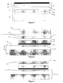
- Figure 1 illustrates the first step of the method according to the invention by showing an epitaxial structure 1 obtained by any suitable process, typically by means of metal organic chemical vapour deposition MOCVD or molecular beam epitaxy MBE techniques.
- the process is carried out on a III-V substrate 10 to obtain first the photodetection p-i-n structure 11 and then the light source or laser n-i-p structure 12. Both structures are stacked.
- the growth is performed on a InP substrate.
- the photodetection structure 11 includes a upper contact layer 110, an absorbing layer 111 and a bottom contact layer 112. As shown in Figure 1 , the photodetector upper contact layer 110 is in the continuation of the substrate 10 and the absorbing layer 111 is located between the upper contact layer 110 and the bottom contact layer 112.
- the light source or laser structure 12 includes an upper contact layer 112, a laser layer 121 and a bottom contact layer 122.
- the thickness of the epitaxy layers is less than 3 ⁇ m when the thickness of the substrate 10 is about 350 ⁇ m.
- photodetector bottom contact layer is also the laser upper contact layer. This reduces the thickness of the epitaxy, and the number of processing steps.
- the structure 1 is then bonded, by means of a die to wafer process for instance, to a SOI wafer 2.
- the SOI wafer 2 includes a Si substrate 20, a layer 21 including a. Si waveguide 210 and a bonding layer 22.
- the structure 2 can be obtained either from:
- the Si waveguide 210 is obtained by hard mask SiOx deposition, photolithography, and etching.
- the waveguide is then covered by SiOx and the surface is planarized by Chemical Mechanical Polishing (CMP) to obtain the bonding layer 22.
- CMP Chemical Mechanical Polishing
- the structure 1 is bonded to the structure 2 in such a way that the laser bottom contact layer 122 is in contact with the bonding layer 22.
- the substrate 10 is then mechanically and chemically removed by any suitable etching process.
- the removal of the substrate can also take place before bonding the structure 1 to the structure 2, but the removal is more difficult to obtain at that stage.
- the photodetector upper contact layer 110 has a composition different from the substrate 10 and thus plays the role of an etch stop layer.
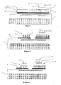
- the structure 3 resulting from this etching is illustrated by figure 3 .
- the photodetector definition can be performed.
- Figure 4 illustrated the resulting structure, which includes the structure 2, the light source or laser structure 12 and a photodetector 4.
- the photodetector comprises a bottom contact layer 42 which is the laser upper contact layer 112, an absorbing layer 41 resulting from layer 111, and an upper contact layer 40 resulting from layer 110.
- the laser geometry can then be defined by dry or wet etching.
- figure 5 which includes the structure 2, the photodetector 4 and the laser 5.
- the laser comprises a bottom contact layer 50 which results from the laser bottom contact layer 122, a laser layer 51 resulting from layer 121, and a upper contact layer 52 resulting from the laser upper contact layer 112.
- the last step of the process according to the invention is illustrated by Figure 6 , and it is an electrode deposition step.
- the electrodes of the photodetector 4 are referenced 43 and 44 while the ones of the laser 5 are referenced 53 and 54.
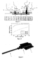
- Figure 7 illustrates how light is generated, guided, and detected in the complete link (forward bias for the laser, reverse bias for the photodetector).
- the laser is a forward biased p-i-n diode, at a current above the threshold current, in order to obtain the laser effect.
- the light emitted by the laser is coupled in the underlying waveguide (F1), then spreads in the waveguide (F2), and finally is coupled in the photodetector which is a reverse biased p-i-n diode (F3).
- the photodetector upper contact layer 110 can be a 100nm thick highly p-doped In 0.53 Ga 0.47 As (lattice matched to InP) layer which is commonly used to take a p type ohmic contact.
- the etching selectivity between the InP substrate 10 and In 0.53 Ga 0.47 As is extremely high with the etching mixture HCl/H2O, 3/1. Therefore, in the frame of the invention, the In 0.53 Ga 0.47 As layer 110 fulfils two functions: it contributes to the definition of the photodetector, but it also has the function of an etch stop layer during substrate removal.
- the structure 3 after removal of the substrate is illustrated on Figure 3 .
- the absorption layer 111 can be 500nm thick and undoped. It is also made of In 0.53 Ga 0.47 As which has a strong absorption (> 4000cm-1) at telecom wavelength (1.3 ⁇ m-1.55 ⁇ m).
- the photodetector bottom contact layer 112 can be a n doped InP layer which defines the bottom of the photodiode (p-i-n structure) and the top of the laser structure (standard n-i-p structure or tunnel junction n-n + -p + -pi-n structure). It is therefore also the laser upper contact layer.
- a tunnel junction (n + -p + ) structure as shown in Figure 7 , a quaternary material such as InGaAsP (energy gap corresponding to 1.3 ⁇ m) lattice matched to InP is a relevant choice.
- the laser layer 121 can be around 400nm thick and composed of an undoped separate confinement heterostructure (so-called SCH) in which active region such as quantum wells or quantum dots are grown.
- the active layer is composed of either InGaAsP or AlGaInAs-based quaternary compounds.
- the laser bottom contact layer 122 can be made of a ⁇ 200nm thick InP layer which is n doped in the case of a tunnel junction approach or p doped for a standard approach.
- the tunnel junction approach is preferred to couple light efficiently from the laser to the waveguide, since holes absorb more light than electrons (the ratio absorption coefficient of the holes/absorption coefficient of the electrons is 10).
- the photodetector definition can be performed.
- This standard process can be photoresist deposition, photolithography or ebeam lithography, or etching.
- the laser geometry can then be defined by dry etching for instance Reactive Ion Etching with CH 4 /H 2 or Inducely Coupled Plasma etching with Cl 2 /H 2 .
- the light coupling between the waveguide and the photodetector region where light will be absorbed is performed either by an evanescent effect or by a guide to guide effect. These two effects will be described thereafter.
- Figure 8 comprises two curves representing the photodetection efficiency as a function of the photodetector length, and for a thickness of the oxide layer, or bonding layer, taken between the waveguide and the epitaxy layers of 100nm (-) or 200nm (---).
- the simulations were carried out with a laser having a thickness of 500nm and a photodetector made of InGaAs and having also a thickness of 500nm and with Au electrodes.
- Figure 8 shows that the coupling efficiency increases when the length of the detector increases and when the thickness of the bonding layer decreases.
- the detector length is typically in the range 20 ⁇ m - 100 ⁇ m. Some diffraction losses can occur at the interfaces where the photodetector is geometrically defined.
- Figure 8 also shows that, as an example, with a bonding layer having a thickness of 100nm, more than 90% of the light spreading in the waveguide is absorbed in less than 40 ⁇ m.
- the coupling by guide to guide effect is used to increase the compactness of the photodetector. As known by a person skilled in the art, this effect can be obtained with a special design of the waveguides.
- the principle of the device can be understood by referring to Figure 9 .
- the photodetector 4 is provided with a guide to guide coupler 6.
- the width of the coupler is much smaller than the one of the photodetector.
- An adiabatic taper 7 is thus provided in the laser source waveguide between the coupler and the photodetector.
- the coupler and the taper are obtained through additional photolithography steps.
- the light of the silicon waveguide is first transferred in the laser source epilayers by a guide to guide effect.
- the phase matching condition between the silicon and the source waveguide is obtained by a correct choice of the source waveguide width.
- Modeling shows that a width of 0.38 ⁇ m for the source waveguide is necessary to have a coupling efficiency of 100 % between the two waveguides for a silicon waveguide of 0.5 ⁇ m width.
- the performance of the photodetector is almost the same when its operation is based on evanescent coupling or on coupling by guide to guide effect.
- a photodetector as illustrated on Figure 9 presents a higher compactness. For a spacing between the two waveguides of 0.2 ⁇ m, the coupling length is about 8 ⁇ m.
- the light is injected in the photodetector epilayers.
- the depth of the layer stack must be chosen in such a way that the fundamental mode profile of the source epilayers waveguide is matching the first order mode of the waveguide in the layer stack part of the photodetector.
- the size of the photodetector can be reduced to 2 ⁇ m large and 10 ⁇ m long.
- a width of 2 ⁇ m is needed.
- An adiabatic taper in the source waveguide is used to enlarge the width of 0.38 ⁇ m to 2 ⁇ m.
- the total length of the device is about 24 ⁇ m and the length of the photodetector is reduced to 10 ⁇ m.
- the small size of the photodetector will lead to a small capacitance for this device, which should allow for a very high frequency operation for such a photodetection device.
- a photonic device can be obtained in which the performances of the light source(s) and of the photodetector(s) can be optimized independently. Indeed, the layers constituting the light source(s) and the photodetector(s) are realized successively and can be adapted to the expected performances. However, the layers are obtained during the same epitaxy and therefore, the process is not complex.
- the process enables to obtain a photonic device in which the light source(s) and the photodetector(s) can be closely positioned. Indeed, it is not necessary to bond independently the light source(s) and the photodetector(s) on the silicon wafer. Therefore, the minimum distance between the light source(s) and the photodetector is not set by the bonding techniques, but by the lithography resolution. The latter is less than 1 ⁇ m.
- epitaxy can be made simpler by designing the photodetection structure and the light source structure with a shared layer.
- this shared layer is the laser upper contact layer and the photodetector bottom contact layer, referenced 112.
- composition of this shared layer can be chosen so that this layer fulfils the function of an etch stop layer during the process according to the invention. This particular choice also makes the process simpler.
- the etching of the layers 122 and 121 is carried out by plasma-etching and not by chemical etching.
- the photodetector upper contact layer 110 can be chosen in order to stop the removal of the substrate during the process according to the invention. This contributes to the simplification of the process.
- the absorbing layer 111 is the upper layer, it can be selectively removed, anywhere it is necessary to do so. It will not impact the laser performances.
- the absorption coefficient of InGaAs material being high, only a small surface is needed to detect the major part of the light emitted by the laser.
- the photodetector layer can be used as monitoring photo diode for the laser.
- InGaAsP or AlGaInAs alloys can also be used when the photodetector bottom contact layer 112 is a InP layer and GaAsN, InGaAs, InGaAsSb, InGaAsSbN, GaAsSb and GaAsSbN can be used when the photodetector bottom contact layer 112 is a GaAs layer.
- the process according to the invention is thus an interesting way of producing photonic integrated circuits (PIC).
Landscapes
- Physics & Mathematics (AREA)
- General Physics & Mathematics (AREA)
- Optics & Photonics (AREA)
- Engineering & Computer Science (AREA)
- Microelectronics & Electronic Packaging (AREA)
- Semiconductor Lasers (AREA)
- Light Receiving Elements (AREA)
Claims (6)
- Procédé de production d'un dispositif photonique comprenant au moins une source de lumière et au moins un photodétecteur sur une structure (2) comprenant une couche de guide d'ondes (210), le procédé comprenant les étapes suivantes :a) la croissance successivement sur un substrat (10) d'une structure de photodétection (11) et d'une structure de source de lumière (12), la structure de photodétection et la structure de source de lumière étant constituées par un empilement de couches, chaque empilement comprenant une couche active (111, 121) entre deux couches de contact (110, 112 ; 112, 122), les couches de la structure de source de lumière étant empilées sur le dessus des couches de la structure de photodétection et les deux structures partageant une de ces couches, cette couche partagée étant une couche de contact de chaque structure,b) le collage de la structure obtenue par l'étape a) à ladite structure de guide d'ondes (2), la structure de source de lumière étant en contact avec ladite structure de guide d'ondes (2) au moyen d'une de ses couches de contact (122),c) l'élimination du substrat (10) de la structure obtenue par l'étape b),d) la gravure de la structure (3) obtenue par l'étape c) pour définir l' au moins un photodétecteur (4),e) la gravure de la structure obtenue par l'étape d) pour définir l'au moins une source de lumière (5), de manière que la couche de contact inférieure du photodétecteur (42), qui est plus proche de la structure de guide d'ondes (2) que la couche active du photodétecteur (41), ait la même structure que la couche de contact supérieure de la source de lumière (52) qui est plus éloignée de la structure de guide d'ondes que la couche active de la source de lumière (51), la couche de contact inférieure du photodétecteur et la couche de contact supérieure de la source de lumière étant obtenues à partir de ladite couche partagée,f) la formation d'électrodes (44, 43 ; 54, 53) sur l'au moins un photodétecteur (4) et sur l'au moins une source de lumière (5).
- Procédé selon la revendication 1, dans lequel la couche partagée (112) arrête la gravure dans l'étape d).
- Procédé selon la revendication 1 ou 2, dans lequel une couche de contact (110) de la structure de photodétection (11) arrête l'élimination du substrat (10) dans l'étape c).
- Procédé selon une des revendications 1 à 3, dans lequel le substrat est un substrat III-V.
- Procédé selon une des revendications 1 à 4, dans lequel l'étape f) est obtenue par dépôt d'une couche d'un matériau conducteur de l'électricité.
- Dispositif photonique comprenant au moins une source de lumière (5) et au moins un photodétecteur (4) sur une structure de guide d'ondes (2), laquelle structure de guide d'ondes comprend une couche de guide d'ondes (210), le photodétecteur et la source de lumière étant constitués par un empilement de couches, chaque empilement comprenant une couche active (51, 41) entre une couche de contact supérieure (52, 40) et une couche de contact inférieure (50, 42), la couche de contact inférieure étant plus proche de la structure de guide d'ondes (2) que la couche active respective (51, 41), dans lequel la couche de contact inférieure de la source de lumière (50) est en contact avec la structure de guide d'ondes (2), et la couche de contact supérieure, de la source de lumière (52) a la même structure que la couche de contact inférieure du photodétecteur (42) et est obtenue à partir d'une couche formée par croissance dans laquelle la couche de contact supérieure de la source de lumière et la couche de contact inférieure du photodétecteur sont fusionnées.
Priority Applications (3)
| Application Number | Priority Date | Filing Date | Title |
|---|---|---|---|
| EP09290077.8A EP2214042B1 (fr) | 2009-02-02 | 2009-02-02 | Procédé de production d'un dispositif photonique et dispositif photonique correspondant |
| PCT/IB2010/000414 WO2010086748A1 (fr) | 2009-02-02 | 2010-02-01 | Procédé de fabrication d'un dispositif photonique et dispositif photonique correspondant |
| US13/147,015 US8676002B2 (en) | 2009-02-02 | 2010-02-01 | Method of producing a photonic device and corresponding photonic device |
Applications Claiming Priority (1)
| Application Number | Priority Date | Filing Date | Title |
|---|---|---|---|
| EP09290077.8A EP2214042B1 (fr) | 2009-02-02 | 2009-02-02 | Procédé de production d'un dispositif photonique et dispositif photonique correspondant |
Publications (2)
| Publication Number | Publication Date |
|---|---|
| EP2214042A1 EP2214042A1 (fr) | 2010-08-04 |
| EP2214042B1 true EP2214042B1 (fr) | 2015-03-11 |
Family
ID=40812241
Family Applications (1)
| Application Number | Title | Priority Date | Filing Date |
|---|---|---|---|
| EP09290077.8A Not-in-force EP2214042B1 (fr) | 2009-02-02 | 2009-02-02 | Procédé de production d'un dispositif photonique et dispositif photonique correspondant |
Country Status (3)
| Country | Link |
|---|---|
| US (1) | US8676002B2 (fr) |
| EP (1) | EP2214042B1 (fr) |
| WO (1) | WO2010086748A1 (fr) |
Families Citing this family (17)
| Publication number | Priority date | Publication date | Assignee | Title |
|---|---|---|---|---|
| US9653639B2 (en) * | 2012-02-07 | 2017-05-16 | Apic Corporation | Laser using locally strained germanium on silicon for opto-electronic applications |
| EP2685297B1 (fr) | 2012-07-13 | 2017-12-06 | Huawei Technologies Co., Ltd. | Procédé de fabrication d'un circuit photonique avec structures actives et passives |
| JP5758359B2 (ja) * | 2012-08-09 | 2015-08-05 | 株式会社東芝 | 光配線デバイスおよびその製造方法 |
| US9322996B2 (en) | 2013-03-07 | 2016-04-26 | Aurrion, Inc. | Simultaneous processing of multiple photonic device layers |
| JP2014215426A (ja) * | 2013-04-25 | 2014-11-17 | 株式会社沖データ | 光電子半導体装置及びその製造方法 |
| WO2015059511A1 (fr) | 2013-10-22 | 2015-04-30 | Commissariat à l'énergie atomique et aux énergies alternatives | Dispositif opto-mécanique comprenant des éléments mécaniques et des filtres optiques pour actionner et/ou détecter le mouvement des éléments |
| EP2866000B1 (fr) * | 2013-10-22 | 2020-03-11 | Commissariat à l'Énergie Atomique et aux Énergies Alternatives | Dispositif optomécanique d'actionnement et/ou de détection du déplacement d'un élément mécanique, notamment pour la détection gravimétrique |
| EP3673517A1 (fr) * | 2017-08-22 | 2020-07-01 | Rockley Photonics Limited | Photodétecteur schottky |
| US10734788B2 (en) | 2018-03-02 | 2020-08-04 | Cisco Technology, Inc. | Quantum dot lasers integrated on silicon submount with mechanical features and through-silicon vias |
| US10461495B2 (en) * | 2018-03-02 | 2019-10-29 | Cisco Technology, Inc. | Substrate technology for quantum dot lasers integrated on silicon |
| US10734785B2 (en) | 2018-03-02 | 2020-08-04 | Cisco Technology, Inc. | Silicon photonics co-integrated with quantum dot lasers on silicon |
| WO2020096950A1 (fr) * | 2018-11-06 | 2020-05-14 | The Regents Of The University Of California | Nitrure d'indium et de gallium à intégration hétérogène sur des circuits intégrés photoniques au silicium |
| US11550099B2 (en) * | 2018-11-21 | 2023-01-10 | The Research Foundation For The State University Of New York | Photonics optoelectrical system |
| US11029466B2 (en) | 2018-11-21 | 2021-06-08 | The Research Foundation For The State University Of New York | Photonics structure with integrated laser |
| TWI851601B (zh) | 2018-11-21 | 2024-08-11 | 紐約州立大學研究基金會 | 光子光電系統及其製造方法 |
| JP7302363B2 (ja) * | 2019-07-31 | 2023-07-04 | 住友電気工業株式会社 | 光半導体素子の製造方法 |
| FR3144325B1 (fr) * | 2022-12-22 | 2026-03-06 | Commissariat Energie Atomique | Système optoélectronique comprenant un transducteur et un guide d'ondes |
Family Cites Families (5)
| Publication number | Priority date | Publication date | Assignee | Title |
|---|---|---|---|---|
| US6706546B2 (en) * | 1998-10-09 | 2004-03-16 | Fujitsu Limited | Optical reflective structures and method for making |
| US6690845B1 (en) * | 1998-10-09 | 2004-02-10 | Fujitsu Limited | Three-dimensional opto-electronic modules with electrical and optical interconnections and methods for making |
| DE60208416T2 (de) * | 2001-10-09 | 2006-06-22 | Infinera Corp., Sunnyvale | Digitale optische netzwerkarchitektur |
| US7116851B2 (en) * | 2001-10-09 | 2006-10-03 | Infinera Corporation | Optical signal receiver, an associated photonic integrated circuit (RxPIC), and method improving performance |
| US20090078963A1 (en) * | 2007-07-09 | 2009-03-26 | Salah Khodja | Nano-optoelectronic chip structure and method |
-
2009
- 2009-02-02 EP EP09290077.8A patent/EP2214042B1/fr not_active Not-in-force
-
2010
- 2010-02-01 WO PCT/IB2010/000414 patent/WO2010086748A1/fr not_active Ceased
- 2010-02-01 US US13/147,015 patent/US8676002B2/en not_active Expired - Fee Related
Also Published As
| Publication number | Publication date |
|---|---|
| WO2010086748A1 (fr) | 2010-08-05 |
| US20120063717A1 (en) | 2012-03-15 |
| EP2214042A1 (fr) | 2010-08-04 |
| US8676002B2 (en) | 2014-03-18 |
Similar Documents
| Publication | Publication Date | Title |
|---|---|---|
| EP2214042B1 (fr) | Procédé de production d'un dispositif photonique et dispositif photonique correspondant | |
| US11550099B2 (en) | Photonics optoelectrical system | |
| Jiao et al. | InP membrane integrated photonics research | |
| US10859764B2 (en) | Integrated active devices with improved optical coupling between active and passive waveguides | |
| US8994004B2 (en) | Hybrid silicon optoelectronic device and method of formation | |
| US10476231B2 (en) | Photonic device comprising a laser optically connected to a silicon waveguide and method for manufacturing such a photonic device | |
| CN103259185B (zh) | 硅激光器-量子阱混合晶片结合的集成平台 | |
| KR102059891B1 (ko) | 집적 도파관 커플러 | |
| KR101594467B1 (ko) | 하이브리드 레이저 | |
| US10641959B1 (en) | Integrated active devices with improved optical coupling to planarized dielectric waveguides | |
| US20190288485A1 (en) | Hybrid Silicon Lasers on Bulk Silicon Substrates | |
| US11209592B2 (en) | Integrated active devices with enhanced optical coupling to dielectric waveguides | |
| US11719883B1 (en) | Integrated GaAs active devices with improved optical coupling to dielectric waveguides | |
| Brouckaert et al. | Compact InAlAs–InGaAs metal–semiconductor–metal photodetectors integrated on silicon-on-insulator waveguides | |
| JP2010263153A (ja) | 半導体集積光デバイス及びその作製方法 | |
| US20190140425A1 (en) | Electro-optical device with lateral electron blocking layer | |
| US12366705B2 (en) | Photonics optoelectrical system | |
| US20230261442A1 (en) | Weak Index Guiding of Interband Lasers Bonded to GaAs Substrates | |
| US12313881B2 (en) | Heterogenously integrated short wavelength photonic platform with optimally minimal reflections | |
| CN111987585B (zh) | 一种硅波导输出激光器 | |
| US20210265806A1 (en) | Selective-area growth of iii-v materials for integration with silicon photonics | |
| Keyvaninia et al. | Demonstration of a novel III-V-on-Si distributed feedback laser | |
| Sabnis et al. | Intimate monolithic integration of chip-scale photonic circuits | |
| US20240072511A1 (en) | Heterogeneous Integration Using a Germanium Handle Substrate | |
| WO2017041812A1 (fr) | Dispositif optoélectronique comprenant un guide d'ondes et un ensemble de nanofils semi-conducteurs, et procédé de fabrication associé |
Legal Events
| Date | Code | Title | Description |
|---|---|---|---|
| PUAI | Public reference made under article 153(3) epc to a published international application that has entered the european phase |
Free format text: ORIGINAL CODE: 0009012 |
|
| AK | Designated contracting states |
Kind code of ref document: A1 Designated state(s): AT BE BG CH CY CZ DE DK EE ES FI FR GB GR HR HU IE IS IT LI LT LU LV MC MK MT NL NO PL PT RO SE SI SK TR |
|
| AX | Request for extension of the european patent |
Extension state: AL BA RS |
|
| 17P | Request for examination filed |
Effective date: 20100914 |
|
| AKX | Designation fees paid |
Designated state(s): AT BE BG CH CY CZ DE DK EE ES FI FR GB GR HR HU IE IS IT LI LT LU LV MC MK MT NL NO PL PT RO SE SI SK TR |
|
| 17Q | First examination report despatched |
Effective date: 20111104 |
|
| RAP1 | Party data changed (applicant data changed or rights of an application transferred) |
Owner name: INTERUNIVERSITAIR MICRO-ELEKTRONICA CENTRUM VZW Owner name: UNIVERSITE DE GAND Owner name: CENTRE NATIONAL DE LA RECHERCHE SCIENTIFIQUE Owner name: COMMISSARIAT A L'ENERGIE ATOMIQUE ET AUX ENERGIES |
|
| RAP1 | Party data changed (applicant data changed or rights of an application transferred) |
Owner name: UNIVERSITE DE GAND Owner name: INTERUNIVERSITAIR MICRO-ELECTRONICA CENTRUM VZW Owner name: CENTRE NATIONAL DE LA RECHERCHE SCIENTIFIQUE Owner name: COMMISSARIAT A L'ENERGIE ATOMIQUE ET AUX ENERGIES |
|
| RAP1 | Party data changed (applicant data changed or rights of an application transferred) |
Owner name: IMEC Owner name: UNIVERSITEIT GENT Owner name: CENTRE NATIONAL DE LA RECHERCHE SCIENTIFIQUE Owner name: COMMISSARIAT A L'ENERGIE ATOMIQUE ET AUX ENERGIES |
|
| GRAP | Despatch of communication of intention to grant a patent |
Free format text: ORIGINAL CODE: EPIDOSNIGR1 |
|
| RIC1 | Information provided on ipc code assigned before grant |
Ipc: G02B 6/13 20060101ALI20140910BHEP Ipc: G02B 6/43 20060101AFI20140910BHEP Ipc: G02B 6/136 20060101ALI20140910BHEP |
|
| INTG | Intention to grant announced |
Effective date: 20140926 |
|
| GRAS | Grant fee paid |
Free format text: ORIGINAL CODE: EPIDOSNIGR3 |
|
| GRAA | (expected) grant |
Free format text: ORIGINAL CODE: 0009210 |
|
| AK | Designated contracting states |
Kind code of ref document: B1 Designated state(s): AT BE BG CH CY CZ DE DK EE ES FI FR GB GR HR HU IE IS IT LI LT LU LV MC MK MT NL NO PL PT RO SE SI SK TR |
|
| REG | Reference to a national code |
Ref country code: GB Ref legal event code: FG4D |
|
| REG | Reference to a national code |
Ref country code: CH Ref legal event code: EP |
|
| REG | Reference to a national code |
Ref country code: IE Ref legal event code: FG4D |
|
| REG | Reference to a national code |
Ref country code: AT Ref legal event code: REF Ref document number: 715650 Country of ref document: AT Kind code of ref document: T Effective date: 20150415 |
|
| REG | Reference to a national code |
Ref country code: DE Ref legal event code: R096 Ref document number: 602009029913 Country of ref document: DE Effective date: 20150423 |
|
| REG | Reference to a national code |
Ref country code: NL Ref legal event code: VDEP Effective date: 20150311 |
|
| REG | Reference to a national code |
Ref country code: NL Ref legal event code: VDEP Effective date: 20150311 |
|
| PG25 | Lapsed in a contracting state [announced via postgrant information from national office to epo] |
Ref country code: FI Free format text: LAPSE BECAUSE OF FAILURE TO SUBMIT A TRANSLATION OF THE DESCRIPTION OR TO PAY THE FEE WITHIN THE PRESCRIBED TIME-LIMIT Effective date: 20150311 Ref country code: LT Free format text: LAPSE BECAUSE OF FAILURE TO SUBMIT A TRANSLATION OF THE DESCRIPTION OR TO PAY THE FEE WITHIN THE PRESCRIBED TIME-LIMIT Effective date: 20150311 Ref country code: ES Free format text: LAPSE BECAUSE OF FAILURE TO SUBMIT A TRANSLATION OF THE DESCRIPTION OR TO PAY THE FEE WITHIN THE PRESCRIBED TIME-LIMIT Effective date: 20150311 Ref country code: NO Free format text: LAPSE BECAUSE OF FAILURE TO SUBMIT A TRANSLATION OF THE DESCRIPTION OR TO PAY THE FEE WITHIN THE PRESCRIBED TIME-LIMIT Effective date: 20150611 Ref country code: HR Free format text: LAPSE BECAUSE OF FAILURE TO SUBMIT A TRANSLATION OF THE DESCRIPTION OR TO PAY THE FEE WITHIN THE PRESCRIBED TIME-LIMIT Effective date: 20150311 Ref country code: SE Free format text: LAPSE BECAUSE OF FAILURE TO SUBMIT A TRANSLATION OF THE DESCRIPTION OR TO PAY THE FEE WITHIN THE PRESCRIBED TIME-LIMIT Effective date: 20150311 |
|
| REG | Reference to a national code |
Ref country code: AT Ref legal event code: MK05 Ref document number: 715650 Country of ref document: AT Kind code of ref document: T Effective date: 20150311 |
|
| REG | Reference to a national code |
Ref country code: LT Ref legal event code: MG4D |
|
| PG25 | Lapsed in a contracting state [announced via postgrant information from national office to epo] |
Ref country code: LV Free format text: LAPSE BECAUSE OF FAILURE TO SUBMIT A TRANSLATION OF THE DESCRIPTION OR TO PAY THE FEE WITHIN THE PRESCRIBED TIME-LIMIT Effective date: 20150311 Ref country code: GR Free format text: LAPSE BECAUSE OF FAILURE TO SUBMIT A TRANSLATION OF THE DESCRIPTION OR TO PAY THE FEE WITHIN THE PRESCRIBED TIME-LIMIT Effective date: 20150612 |
|
| PG25 | Lapsed in a contracting state [announced via postgrant information from national office to epo] |
Ref country code: NL Free format text: LAPSE BECAUSE OF FAILURE TO SUBMIT A TRANSLATION OF THE DESCRIPTION OR TO PAY THE FEE WITHIN THE PRESCRIBED TIME-LIMIT Effective date: 20150311 |
|
| PG25 | Lapsed in a contracting state [announced via postgrant information from national office to epo] |
Ref country code: SK Free format text: LAPSE BECAUSE OF FAILURE TO SUBMIT A TRANSLATION OF THE DESCRIPTION OR TO PAY THE FEE WITHIN THE PRESCRIBED TIME-LIMIT Effective date: 20150311 Ref country code: CZ Free format text: LAPSE BECAUSE OF FAILURE TO SUBMIT A TRANSLATION OF THE DESCRIPTION OR TO PAY THE FEE WITHIN THE PRESCRIBED TIME-LIMIT Effective date: 20150311 Ref country code: RO Free format text: LAPSE BECAUSE OF FAILURE TO SUBMIT A TRANSLATION OF THE DESCRIPTION OR TO PAY THE FEE WITHIN THE PRESCRIBED TIME-LIMIT Effective date: 20150311 Ref country code: PT Free format text: LAPSE BECAUSE OF FAILURE TO SUBMIT A TRANSLATION OF THE DESCRIPTION OR TO PAY THE FEE WITHIN THE PRESCRIBED TIME-LIMIT Effective date: 20150713 Ref country code: EE Free format text: LAPSE BECAUSE OF FAILURE TO SUBMIT A TRANSLATION OF THE DESCRIPTION OR TO PAY THE FEE WITHIN THE PRESCRIBED TIME-LIMIT Effective date: 20150311 |
|
| PG25 | Lapsed in a contracting state [announced via postgrant information from national office to epo] |
Ref country code: IS Free format text: LAPSE BECAUSE OF FAILURE TO SUBMIT A TRANSLATION OF THE DESCRIPTION OR TO PAY THE FEE WITHIN THE PRESCRIBED TIME-LIMIT Effective date: 20150711 Ref country code: PL Free format text: LAPSE BECAUSE OF FAILURE TO SUBMIT A TRANSLATION OF THE DESCRIPTION OR TO PAY THE FEE WITHIN THE PRESCRIBED TIME-LIMIT Effective date: 20150311 Ref country code: AT Free format text: LAPSE BECAUSE OF FAILURE TO SUBMIT A TRANSLATION OF THE DESCRIPTION OR TO PAY THE FEE WITHIN THE PRESCRIBED TIME-LIMIT Effective date: 20150311 |
|
| REG | Reference to a national code |
Ref country code: DE Ref legal event code: R097 Ref document number: 602009029913 Country of ref document: DE |
|
| PG25 | Lapsed in a contracting state [announced via postgrant information from national office to epo] |
Ref country code: IT Free format text: LAPSE BECAUSE OF FAILURE TO SUBMIT A TRANSLATION OF THE DESCRIPTION OR TO PAY THE FEE WITHIN THE PRESCRIBED TIME-LIMIT Effective date: 20150311 |
|
| PLBE | No opposition filed within time limit |
Free format text: ORIGINAL CODE: 0009261 |
|
| STAA | Information on the status of an ep patent application or granted ep patent |
Free format text: STATUS: NO OPPOSITION FILED WITHIN TIME LIMIT |
|
| PG25 | Lapsed in a contracting state [announced via postgrant information from national office to epo] |
Ref country code: DK Free format text: LAPSE BECAUSE OF FAILURE TO SUBMIT A TRANSLATION OF THE DESCRIPTION OR TO PAY THE FEE WITHIN THE PRESCRIBED TIME-LIMIT Effective date: 20150311 |
|
| 26N | No opposition filed |
Effective date: 20151214 |
|
| PG25 | Lapsed in a contracting state [announced via postgrant information from national office to epo] |
Ref country code: SI Free format text: LAPSE BECAUSE OF FAILURE TO SUBMIT A TRANSLATION OF THE DESCRIPTION OR TO PAY THE FEE WITHIN THE PRESCRIBED TIME-LIMIT Effective date: 20150311 |
|
| REG | Reference to a national code |
Ref country code: FR Ref legal event code: PLFP Year of fee payment: 8 |
|
| PG25 | Lapsed in a contracting state [announced via postgrant information from national office to epo] |
Ref country code: BE Free format text: LAPSE BECAUSE OF NON-PAYMENT OF DUE FEES Effective date: 20160229 |
|
| PG25 | Lapsed in a contracting state [announced via postgrant information from national office to epo] |
Ref country code: BE Free format text: LAPSE BECAUSE OF FAILURE TO SUBMIT A TRANSLATION OF THE DESCRIPTION OR TO PAY THE FEE WITHIN THE PRESCRIBED TIME-LIMIT Effective date: 20150311 |
|
| PG25 | Lapsed in a contracting state [announced via postgrant information from national office to epo] |
Ref country code: LU Free format text: LAPSE BECAUSE OF FAILURE TO SUBMIT A TRANSLATION OF THE DESCRIPTION OR TO PAY THE FEE WITHIN THE PRESCRIBED TIME-LIMIT Effective date: 20160202 Ref country code: MC Free format text: LAPSE BECAUSE OF FAILURE TO SUBMIT A TRANSLATION OF THE DESCRIPTION OR TO PAY THE FEE WITHIN THE PRESCRIBED TIME-LIMIT Effective date: 20150311 |
|
| REG | Reference to a national code |
Ref country code: CH Ref legal event code: PL |
|
| PG25 | Lapsed in a contracting state [announced via postgrant information from national office to epo] |
Ref country code: CH Free format text: LAPSE BECAUSE OF NON-PAYMENT OF DUE FEES Effective date: 20160229 Ref country code: LI Free format text: LAPSE BECAUSE OF NON-PAYMENT OF DUE FEES Effective date: 20160229 |
|
| REG | Reference to a national code |
Ref country code: IE Ref legal event code: MM4A |
|
| PG25 | Lapsed in a contracting state [announced via postgrant information from national office to epo] |
Ref country code: IE Free format text: LAPSE BECAUSE OF NON-PAYMENT OF DUE FEES Effective date: 20160202 |
|
| REG | Reference to a national code |
Ref country code: FR Ref legal event code: PLFP Year of fee payment: 9 |
|
| PG25 | Lapsed in a contracting state [announced via postgrant information from national office to epo] |
Ref country code: MT Free format text: LAPSE BECAUSE OF FAILURE TO SUBMIT A TRANSLATION OF THE DESCRIPTION OR TO PAY THE FEE WITHIN THE PRESCRIBED TIME-LIMIT Effective date: 20150311 |
|
| REG | Reference to a national code |
Ref country code: FR Ref legal event code: PLFP Year of fee payment: 10 |
|
| PG25 | Lapsed in a contracting state [announced via postgrant information from national office to epo] |
Ref country code: HU Free format text: LAPSE BECAUSE OF FAILURE TO SUBMIT A TRANSLATION OF THE DESCRIPTION OR TO PAY THE FEE WITHIN THE PRESCRIBED TIME-LIMIT; INVALID AB INITIO Effective date: 20090202 Ref country code: CY Free format text: LAPSE BECAUSE OF FAILURE TO SUBMIT A TRANSLATION OF THE DESCRIPTION OR TO PAY THE FEE WITHIN THE PRESCRIBED TIME-LIMIT Effective date: 20150311 |
|
| PG25 | Lapsed in a contracting state [announced via postgrant information from national office to epo] |
Ref country code: MK Free format text: LAPSE BECAUSE OF FAILURE TO SUBMIT A TRANSLATION OF THE DESCRIPTION OR TO PAY THE FEE WITHIN THE PRESCRIBED TIME-LIMIT Effective date: 20150311 Ref country code: MT Free format text: LAPSE BECAUSE OF FAILURE TO SUBMIT A TRANSLATION OF THE DESCRIPTION OR TO PAY THE FEE WITHIN THE PRESCRIBED TIME-LIMIT Effective date: 20160229 Ref country code: TR Free format text: LAPSE BECAUSE OF FAILURE TO SUBMIT A TRANSLATION OF THE DESCRIPTION OR TO PAY THE FEE WITHIN THE PRESCRIBED TIME-LIMIT Effective date: 20150311 |
|
| PG25 | Lapsed in a contracting state [announced via postgrant information from national office to epo] |
Ref country code: BG Free format text: LAPSE BECAUSE OF FAILURE TO SUBMIT A TRANSLATION OF THE DESCRIPTION OR TO PAY THE FEE WITHIN THE PRESCRIBED TIME-LIMIT Effective date: 20150311 |
|
| PGFP | Annual fee paid to national office [announced via postgrant information from national office to epo] |
Ref country code: FR Payment date: 20210226 Year of fee payment: 13 |
|
| PGFP | Annual fee paid to national office [announced via postgrant information from national office to epo] |
Ref country code: DE Payment date: 20210209 Year of fee payment: 13 Ref country code: GB Payment date: 20210216 Year of fee payment: 13 |
|
| REG | Reference to a national code |
Ref country code: DE Ref legal event code: R119 Ref document number: 602009029913 Country of ref document: DE |
|
| GBPC | Gb: european patent ceased through non-payment of renewal fee |
Effective date: 20220202 |
|
| PG25 | Lapsed in a contracting state [announced via postgrant information from national office to epo] |
Ref country code: FR Free format text: LAPSE BECAUSE OF NON-PAYMENT OF DUE FEES Effective date: 20220228 |
|
| PG25 | Lapsed in a contracting state [announced via postgrant information from national office to epo] |
Ref country code: GB Free format text: LAPSE BECAUSE OF NON-PAYMENT OF DUE FEES Effective date: 20220202 Ref country code: DE Free format text: LAPSE BECAUSE OF NON-PAYMENT OF DUE FEES Effective date: 20220901 |