EP2214285A2 - Ladungskontrollschaltung und die Ladung kontrollierende integrierte Halbleiterschaltung - Google Patents
Ladungskontrollschaltung und die Ladung kontrollierende integrierte Halbleiterschaltung Download PDFInfo
- Publication number
- EP2214285A2 EP2214285A2 EP09003916A EP09003916A EP2214285A2 EP 2214285 A2 EP2214285 A2 EP 2214285A2 EP 09003916 A EP09003916 A EP 09003916A EP 09003916 A EP09003916 A EP 09003916A EP 2214285 A2 EP2214285 A2 EP 2214285A2
- Authority
- EP
- European Patent Office
- Prior art keywords
- temperature
- voltage
- current
- output
- charging current
- Prior art date
- Legal status (The legal status is an assumption and is not a legal conclusion. Google has not performed a legal analysis and makes no representation as to the accuracy of the status listed.)
- Withdrawn
Links
Images


Classifications
-
- H—ELECTRICITY
- H02—GENERATION; CONVERSION OR DISTRIBUTION OF ELECTRIC POWER
- H02J—ELECTRIC POWER NETWORKS; CIRCUIT ARRANGEMENTS OR SYSTEMS FOR SUPPLYING OR DISTRIBUTING ELECTRIC POWER; SYSTEMS FOR STORING ELECTRIC ENERGY
- H02J7/00—Circuit arrangements for charging or discharging batteries or for supplying loads from batteries
- H02J7/90—Regulation of charging or discharging current or voltage
- H02J7/971—Regulation of charging or discharging current or voltage the charge cycle being controlled or terminated in response to non-electric parameters
- H02J7/975—Regulation of charging or discharging current or voltage the charge cycle being controlled or terminated in response to non-electric parameters in response to temperature
Definitions
- the present invention relates to a temperature rise suppressing technique of a secondary battery charging apparatus, and to a technique effective for the use of, for example, a charge control circuit and a charge controlling semiconductor integrated circuit (IC) equipped with the charge control circuit.
- IC semiconductor integrated circuit
- a secondary battery charging apparatus uses an IC equipped with a charge control circuit to control a charging current for suppressing an unusual temperature rise in a battery or the inner part of an apparatus.
- a charging apparatus for example, the invention described in Japanese Patent Application Laid-Open Publication No. 2001-145274 exists.
- the invention provides a temperature detection unit in the inner part or in the neighborhood of a heat generating part the temperature of which rises most or a part having the smallest temperature margin, and if an output of the temperature detection unit exceeds a predetermined temperature, then the invention controls the charging current to a secondary battery to decrease or stop the charging current.
- some charging apparatus are provided with the function of suppressing any temperature rises by providing a temperature detecting element on a chip in order to prevent the lowering of the reliability and further the occurrence of troubles of the charging apparatus owing to the heat generation of charge controlling ICs themselves for controlling charging currents.
- the conventional temperature rise suppressing technique of a charge controlling IC is only a simple one to break a charging current by turning off a current controlling transistor when a chip temperature exceeds a predetermined temperature, such as 150°C.
- the control method can suppress the chip temperature not to exceed the set temperature by repeating the cycle of: temperature rise - charging current breaking - temperature lowering - charging current reopening - temperature rise.
- the control method since the control method completely breaks the charging current when the chip temperature exceeds the predetermined temperature, such as 150°C, the control method has the apprehension of causing the chattering phenomenon of: current breaking - current reopening - current breaking - current reopening because a large current abruptly flows through a current controlling transistor at the time of reopening a charging current next owing to a delay in response of a feedback control loop. Moreover, it becomes clear that there is the problem of the apprehension of causing the characteristic degradation of a secondary battery and therefore shortening a battery life owing to the sudden influx of a large current into the secondary battery at the time of current reopening.
- the present invention is directed to enable the avoidance of the causing of a chattering phenomenon of the turning on and off of a current owing to the seesaw movement of the temperature of a monitoring object in a charge control circuit and a charge controlling IC, both equipped with the function of controlling a charging current according to the temperature of a monitoring chip and the like.
- the present invention is also directed to enable the prevention of the deterioration of the characteristics of a secondary battery owing to the sudden influx of a large current into the secondary battery at the time of current reopening in a charge control circuit and a charge controlling IC, both equipped with the function of controlling the turning on and off of a charging current according to the temperature of a monitoring chip and the like.
- a first aspect of the present invention is a charge control circuit equipped with a function of controlling a charging current to be supplied to a secondary battery, comprising:
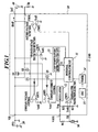
- FIG. 1 shows the schematic configuration of an embodiment of a charge controlling IC of a secondary battery to which the present invention can be suitably applied.
- the charge controlling IC 10 of this embodiment is equipped with a voltage input terminal VIN, to which a direct-current voltage is input from a direct-current power supply 20, such as an external AC adaptor, a battery terminal BAT, to which a secondary battery 40, such as a charging object lithium ion battery, is connected, a current controlling transistor Q1 provided between the voltage input terminal VIN and the battery terminal BAT, and a constant voltage control amplifier AMP1 to compare a battery voltage Vbat and a reference voltage Vref1 for performing constant voltage control to generate a gate control voltage of the transistor Q1.
- a direct-current power supply 20 such as an external AC adaptor
- a battery terminal BAT to which a secondary battery 40, such as a charging object lithium ion battery
- a current controlling transistor Q1 provided between the voltage input terminal VIN and the battery terminal BAT
- a constant voltage control amplifier AMP1 to compare a battery voltage Vbat and a reference voltage Vref1 for performing constant voltage control to generate a gate control voltage of the transistor Q
- the charge controlling IC 10 is equipped with a monitoring transistor Q2, an external terminal PROG, and a constant current controlling amplifier AMP2.
- the monitoring transistor Q2 has the size of 1/N of that of the transistor Q1, a source terminal connected to the voltage input terminal VIN, and a control terminal (gate terminal), to which the same voltage as the one applied to the transistor Q1 is applied, in order to perform current control by detecting a current in proportion to the current flowing through the transistor Q1.
- the drain terminal of the transistor Q2 is connected to the external terminal PROG, and an external resistor Rp can be connected to the external terminal PROG on the outside of the charge controlling IC 10.
- the constant current controlling amplifier AMP2 compares the voltage of the terminal PROG and a reference voltage Vcref to generate a gate control voltage of the transistor Q1 in order to perform constant current control.
- the charge controlling IC 10 of the present embodiment is equipped with comparators CMP1, CMP2, and CMP3, and an internal control circuit 11.
- the comparator CMP1 compares a reference voltage Vref2 of, e.g. 5.8 V, and a direct-current voltage Vin input into the voltage input terminal VIN from the outside to detect abnormality in order to protect the chip from the direct-current voltage Vin.
- the comparator CMP2 compares the voltage at the battery terminal BAT and a reference voltage Vref3.
- the comparator CMP3 compares the voltage at an external terminal TH, to which a temperature sensor 50, such as a thermistor, to detect the temperature in the neighborhood of the secondary battery 40 and the like are connected, and a reference voltage Vref4.
- the internal control circuit 11 judges whether the voltage of the monitoring object secondary battery 40 is an unusual voltage or not on the basis of the outputs of these comparators CMP1 ⁇ CMP3. In the case of the unusual voltage, the internal control circuit 11 generates and outputs a voltage for controlling the gate of a transistor Q3 of an open collector, the drain of which is connected to the gate of the transistor Q1, in order to turn off the current controlling transistor Q1.
- the charge controlling IC 10 is provided with a regulator 12 to generate a constant voltage Vreg, which has no temperature dependency, and a chip temperature detection circuit 13 to detect a chip temperature.
- the chip temperature detection circuit 13 generates a signal to turn on the switching transistor Q3 when the chip temperature detection circuit 13 detects an unusual temperature, and the chip temperature detection circuit 13 generates the reference voltage Vcref to be supplied to the constant current controlling amplifier AMP2 according to a detected temperature.
- the reference voltage Vref4 is generated by dividing the constant voltage Vreg generated by the regulator 12 with resistors R1 and R2. Moreover, the constant voltage Vreg is output to an external terminal VREG, to which a terminal of an external resistor Rt is connected, which external resistor Rt is connected to the temperature sensor 50 in series at the other terminal thereof. Furthermore, the charge controlling IC 10 is provided with a timer circuit 14 and an oscillating circuit 15.
- the timer circuit 14 is composed of a counter to time the time for managing a preliminary charging time, a rapid charging time, and the like.
- the oscillating circuit 15 generates an oscillated signal of a frequency, such as 64 kHz.
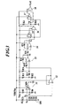
- FIG. 3 shows a concrete circuit configuration example of the chip temperature detection circuit 13.
- the chip temperature detection circuit 13 of this embodiment includes a thermal shut-down detecting circuit 31.
- the thermal shut-down detecting circuit 31 includes a chip temperature detecting element SNS, a constant current source CS, resistors R3 and R4, and a comparator CMP0.
- the chip temperature detecting element SNS is composed of four diodes D1 ⁇ D4 connected in series with each other. The diodes D1 ⁇ D4 are formed on the chip and severally have a negative temperature characteristic.
- the constant current source CS is used to flow a current through the diode row.
- the resistors R3 and R4 divide the constant voltage Vreg.
- the comparator CMP0 has a hysteresis characteristic.
- the current I0 of the constant current source CS and the resistance ratio of the resistors R3 and R4 are set so that the voltage V1 may become larger than 4 ⁇ (forward voltage VF of each of the diodes D1 ⁇ D4) when the chip temperature becomes higher than 140°C. Consequently, when the chip temperature becomes higher than 140°C, the output TS of the comparator CMP0 changes to the high level, and the internal control circuit 11 detects the change to output a voltage to turn off the transistor Q3. Thereby, the current controlling transistor Q1 is turned off, and the charging current to be supplied to the secondary battery 40 is configured to be broken.
- the diodes D1 ⁇ D4 as the chip temperature detecting element SNS is desirably formed in the neighborhood of the current controlling transistor Q1, the heat generation quantity of which is the largest among all of the transistors Q1 ⁇ Q3.
- the chip temperature detecting element corresponds to a temperature detecting unit for monitoring a temperature in the charge controlling IC (charge control circuit).
- the chip temperature detection circuit 13 is equipped with a voltage follower 32, a subtraction circuit 33, and an inverting amplifier 34.
- the voltage follower 32 performs the impedance conversion of the electric potential Va at the node Na to output the converted electric potential.
- the subtraction circuit 33 receives the input of the electric potential determined by the output electric potential of the voltage follower 32 and a resistor circuit composed of resistors R11 ⁇ R14.
- the inverting amplifier 34 performs the inverting amplification of the output electric potential Vb of the subtraction circuit 33.
- a comparator 35, a selector 36, a comparator 37, and a selector 38 are provided at the subsequent stage of the inverting amplifier 34.
- the comparator 35 compares the output electric potential Vc of the inverting amplifier 34 and the constant voltage Vreg.
- the selector 36 is controlled on the basis of the output of the comparator 35 and transmits either of the output of the inverting amplifier 34 and the constant voltage Vreg (2.5 V) to the subsequent stage.
- the comparator 37 compares the output electric potential Vc of the inverting amplifier 34 and the voltage Vd obtained by dividing the constant voltage Vreg with resistors R21 and R22.
- the selector 38 is controlled on the basis of the output of the comparator 37 and outputs either of the output of the selector 36 and the voltage Vd as the reference voltage Vcref.
- the voltage Vd is set as the electric potential such as 0.5 V.
- the electric potential Va of the node Na changes along a straight line indicating the gradual lowering of the electric potential Va as the temperature becomes higher as shown by a broken line A in FIG. 4A .
- the electric potential Va is determined to be, for example, 2.27 V when the chip temperature is 90°C.
- the subtraction circuit 33 since the subtraction circuit 33 outputs the electric potential that is a difference obtained by subtracting the electric potential Va from the electric potential determined by the resistor circuit composed of the resistors R11 ⁇ R14, the output electric potential Vb changes along a straight line indicating the gradual rising of the output electric potential Vb as the temperature becomes higher as shown by a solid line B in FIG. 4A .
- the resistance values of the resistors R11 ⁇ R14 are determined so that the output electric potential Vb, which is determined by the resistance ratios of these resistors R11 ⁇ R14, may be 2.5 V when the chip temperature is 90°C.
- the output electric potential Vc of the inverting amplifier 34 changes along a straight line indicating the passing-through of a point of 2.5 V at the time of the chip temperature of 90°C and indicating the gradual lowering of the output electric potential Vc as the temperature becomes higher as shown by an alternate long and short dash line C in FIG. 4B .
- the resistance ratio of the input resistor R31 and the feedback resistor R32 of the inverting amplifier 34 is set so that the output electric potential Vc of the inverting amplifier 34 becomes 0.5 V when the chip temperature is 100°C.
- the selector 36 at the subsequent stage selects the constant voltage Vreg, which is 2.5 V, when the output electric potential Vc of the inverting amplifier 34 is higher than 2.5 V. Moreover, the selector 36 selects the output electric potential Vc of the inverting amplifier 34 when the output electric potential Vc is lower than 2.5 V. Furthermore, the selector 38 selects the output electric potential Vc of the inverting amplifier 34 when the output electric potential Vc is higher than 0.5 V. Moreover, the selector 38 selects the voltage Vd, which is 0.5 V, when the output electric potential Vc of the inverting amplifier 34 is lower than 0.5 V.
- the output reference voltage Vcref is the constant of 2.5 V when the temperature is 90°C or lower; the output reference voltage Vcref changes along a straight line indicating the gradual lowering of the output reference voltage Vcref as the temperature becomes higher in the range of the temperature of from 90°C to 100°C; and the output reference voltage Vcref is the constant of 0.5 V when the temperature is 100°C or higher, as shown in Fig. 4C .
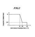
- a charging current IBAT supplied to the secondary battery 40 by the transistor Q1 is controlled so as to be the constant of 0.8 C when the temperature is 90°C or lower, to change along a straight line indicating the gradual lowering of the charging current IBAT as the temperature rises when the temperature is within a range of from 90°C to 100°C, to be the constant of 0.2 C when the temperature is within a range of from 100°C to 140°C, and to be zero when the temperature is 140°C or higher, as shown in FIG. 2 .
- the charging of 0.8 C means to charge the secondary battery 40 with a current value of 80% of a rated current (1 C), which is determined by the characteristics of the secondary battery 40, here.
- the reason why the charging current IBAT is controlled to be the constant of not 1 C but 0.8 C is that the deterioration of the secondary battery 40 caused by the repetition of charging is considered.
- the charging current IBAT is small, then the charging time becomes longer. Consequently, it is desirable to perform the charging with an arbitrary constant current within a range of from 0.7 C to 1 C when the temperature is 90°C or lower in connection with the charging time.
- the temperatures of 90°C and 100°C which give the timing of switching the control, are determined according to the characteristics of the IC to be used and the secondary battery 40 of the charging object, and consequently it is needless to say that the present invention is not limited to such temperatures.
- the temperature range in which the charging current IBAT is changed is set to the range of from 90°C to 100°C in the embodiment described above, the range is not limited to the above one.
- the lower limit temperature of a desirable temperature range is within a range of from 80°C to 100°C, and the upper limit temperature of the desirable temperature range is within a range of 90°C to 120°C.
- the temperature difference of the temperature range is 5°C or more and 20°C or less, and the furthermore desirable temperature difference is 8°C or more and 15°C or less.
- the charging current IBAT is changed from 0.8 C to 0.2 C during a temperature change of 10°C in the embodiment described above, that is, the current rate of change is 0.06 C/°C, but the current rate of change is not limited to this example.
- the desirable current rate of change is within a range of from 0.04 C/°C to 0.08 C/°C. By setting the current rate of change to such a condition, the chip temperature of under charging can be kept in a desired range.
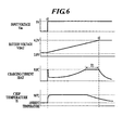
- the charging operation (see FIG. 6 ) of the charge controlling IC 10 of the present embodiment which includes the chip temperature detection circuit 13 as shown in FIG. 3 and performs the temperature current control as shown in FIG. 2 , is described while comparing the charging operation with that (see FIG. 5 ) of the charge control circuit having only the thermal shut-down detecting circuit.
- the thermal shut-down detection is the function of fail safe, which rarely operate in an ordinary charging operation, and the following description will be performed on the supposition that no thermal shut-down is caused.
- the chip temperature in FIG. 6 is a mean temperature of the chip, and the local chip temperature at the position where the temperature detecting diodes D1 ⁇ D4 are formed is higher than the chip temperature shown in FIG. 6 .
- the charging current IBAT of 0.8 C begins to flow immediately after the application of an input direct-current voltage Vin from an adaptor or the like (timing t1) ; a battery voltage VBAT gradually rises by the charging of constant current control; and the constant current control is changed to constant voltage control when the battery voltage VBAT reaches a predetermined constant voltage of 4. 2 V or the like (timing t2).
- the charging current IBAT decreases, and the chip temperature also lowers.
- the thermal shut-down detecting circuit 31 operates to break the charging current IBAT in such a case.
- the charging current IBAT of 0.8 C once flows by the application of the input direct-current voltage Vin (timing t1), but the charging current IBAT is decreased when the chip temperature rises by the charging current IBAT to exceed 90°C. Consequently, the charging is performed in the neighborhood of the chip temperature of 90°C.
- the charging operation changes to the one by the constant current control (in period T1).
- the battery voltage VBAT reaches the predetermined constant voltage, such as 4.2 V, after that, then the charging is switched to the one by the constant voltage control (timing t2) .
- the following control is performed after the change of the charging to that by the constant voltage control. That is, the end of the charging is judged after an elapse of a predetermined time by the use of the timer circuit 14.
- the decrease is monitored, and the end of the charging is judged at the time when the charging current IBAT becomes, for example, 0.1 C or less, or the time point after a predetermined time of the reaching of the charging current IBAT to 0.1 C. Then the current controlling transistor Q1 is turned off.
- the charging current IBAT decreases, and consequently the rise of the chip temperature is suppressed. Consequently, the fail safe function by the thermal shut-down detecting circuit rarely operates, and the occurrence of the chattering phenomenon of sudden chip temperature rise and charging current breaking owing to the breaking and reopening of the charging current IBAT by chip temperature rising is avoided. Consequently, the situation in which the sudden influx of a large current into the secondary battery 40 at the time of current reopening advances the characteristic degradation of the secondary battery 40 can be also prevented.
- the present invention is not limited to the aforesaid embodiment, and various changes can be performed on the basis of the spirit of the present invention.
- the diodes D1 ⁇ D4 are used as the chip temperature detecting element SNS in the embodiment described above
- the PN junctions between the bases and the emitters of NPN transistors may be used as the chip temperature detecting element SNS.
- the chip temperature detecting element SNS is provided to perform temperature control against the rise of the chip temperature in the embodiment described above, the current control described in the embodiment described above may be performed in accordance with a voltage from the thermistor to detect a battery temperature.
- the chip temperature detection circuit 13 in FIG. 3 is provided with the comparators 35 and 37 and the selectors 36 and 38 in order to output the voltages of 2.5 V (constant) at 90°C or less and 0.5 V (constant) at 100°C or more
- the chip temperature detection circuit 13 may be configured to be provided with a clamp section composed of a diode or the like in place of the comparators 35 and 37 and the selector 36 and 38 to clamp output voltages, and to output the voltage of the output waveform similar to that of the embodiment.
- a first aspect of the present invention is a charge control circuit equipped with a function of controlling a charging current to be supplied to a secondary battery, comprising:
- the charge controlling semiconductor integrated circuit comprises:
- the charging current is decreased and it becomes difficult for the monitored temperature, such as the chip temperature, to rise when the monitored temperature becomes the predetermined temperature or more, which predetermined temperature is lower than the set temperature of breaking the charging current, the occurrence of the chattering phenomenon of turning on and off the charging current can be avoided.
- the current reopening frequency of a sudden influx of a large current into the secondary battery can be decreased, and thereby the characteristic degradation of the secondary battery can be prevented.
- the charge controlling semiconductor integrated circuit further comprises a constant current controlling amplifier for controlling a control voltage so that a voltage according to an output charging current may be fed back and a constant current may flow through the current controlling transistor, wherein the charge controlling semiconductor integrated circuit is configured so that an output voltage of the chip temperature detection circuit may be supplied to the constant current controlling amplifier as a reference side voltage.
- the secondary battery can be charged by the predetermined current within the range in which the chip temperature does not exceed the predetermined temperature.
- the charge controlling semiconductor integrated circuit is configured so that the lower limit temperature of the temperature range may be within a range of from 80°C to 100°C, the upper limit temperature of the temperature range may be within a range of from 90°C to 120°C, and a temperature difference of the temperature range may be within a range of from 5°C to 20°C, both inclusive.
- the charge controlling semiconductor integrated circuit is configured so that a rate of change of the charging current in the temperature range may be within a range of from 0.04 C/°C to 0.08 C/°C. Thereby, the chip temperature can be kept in the predetermined range in ordinary charging.
- the charge controlling semiconductor integrated circuit is configured so that the chip temperature detection circuit may be provided with a voltage comparing circuit to output a signal to control the current controlling transistor not to flow any currents therethrough when a voltage generated by the temperature detecting element becomes lower than a predetermined constant voltage or higher than a predetermined constant voltage. Thereby, the charging current can be broken when the chip temperature becomes unusually high.
- the charge controlling semiconductor integrated circuit is configured, so as to be provided with a current monitoring transistor, which has the same structure as that of the current controlling transistor but is formed to be smaller in size than that of the current controlling transistor, the current monitoring transistor being subjected to the application of the same control voltage as that of the current controlling transistor, so that a voltage generated by the current monitoring transistor is fed back to the constant current controlling amplifier and a control voltage according to a potential difference between the fed back voltage and the reference side voltage is generated to be supplied to the current controlling transistor.
- a current monitoring transistor which has the same structure as that of the current controlling transistor but is formed to be smaller in size than that of the current controlling transistor, the current monitoring transistor being subjected to the application of the same control voltage as that of the current controlling transistor, so that a voltage generated by the current monitoring transistor is fed back to the constant current controlling amplifier and a control voltage according to a potential difference between the fed back voltage and the reference side voltage is generated to be supplied to the current controlling transistor.
- the power loss of the charge controlling semiconductor integrated circuit can be decreased in comparison with the case of connecting a resistor in series with the current controlling transistor.
- the charge controlling semiconductor integrated circuit may be configured so as to further comprise:
- the charge controlling semiconductor integrated circuit can perform charging at a predetermined low voltage when the chip temperature is higher than the temperature range.
- the charge controlling semiconductor integrated circuit is configured so that the chip temperature detection circuit may include:
- a charge control circuit capable of charging in a desired temperature range of the chip temperature thereof can be designed comparatively easily.
- the present invention in a charge control circuit or a charge controlling IC that is equipped with the function of controlling a charging current according to the temperature of a monitored chip or the like, the occurrence of a chattering phenomenon of turning on and off the charging current by a seesaw movement of the temperature of a monitoring object can be avoided. Moreover, the present invention also has the advantage capable of preventing the deterioration of the characteristics of the secondary battery owing to the sudden influx of a large current into the secondary battery at the time of current reopening.
- the present invention is not limited such an example, but the present invention can be applied to a direct-current power supply circuit, such as a DC-DC converter and a low saturating type series regulator (LDO), and a multi-function power source controlling IC, such as a power management IC equipped with a plurality of power source series circuits, such as a white light emitting diode (WLED) in addition to the charge control circuit of a secondary battery.
- a direct-current power supply circuit such as a DC-DC converter and a low saturating type series regulator (LDO)
- LDO low saturating type series regulator
- WLED white light emitting diode
Landscapes
- Engineering & Computer Science (AREA)
- Power Engineering (AREA)
- Charge And Discharge Circuits For Batteries Or The Like (AREA)
- Secondary Cells (AREA)
Applications Claiming Priority (1)
| Application Number | Priority Date | Filing Date | Title |
|---|---|---|---|
| JP2008075881A JP5309641B2 (ja) | 2008-03-24 | 2008-03-24 | 充電制御用半導体集積回路 |
Publications (1)
| Publication Number | Publication Date |
|---|---|
| EP2214285A2 true EP2214285A2 (de) | 2010-08-04 |
Family
ID=41088274
Family Applications (1)
| Application Number | Title | Priority Date | Filing Date |
|---|---|---|---|
| EP09003916A Withdrawn EP2214285A2 (de) | 2008-03-24 | 2009-03-18 | Ladungskontrollschaltung und die Ladung kontrollierende integrierte Halbleiterschaltung |
Country Status (4)
| Country | Link |
|---|---|
| US (1) | US8450982B2 (de) |
| EP (1) | EP2214285A2 (de) |
| JP (1) | JP5309641B2 (de) |
| CN (1) | CN101546920B (de) |
Families Citing this family (28)
| Publication number | Priority date | Publication date | Assignee | Title |
|---|---|---|---|---|
| TWI422847B (zh) * | 2010-09-01 | 2014-01-11 | Univ Nat Chiao Tung | 全晶片上寬工作電壓溫度製程電壓的感測系統 |
| JP5605143B2 (ja) * | 2010-10-01 | 2014-10-15 | ミツミ電機株式会社 | 電流制御回路 |
| US8542055B2 (en) * | 2010-12-23 | 2013-09-24 | Fairchild Semiconductor Corporation | Multi-level control for pass transistor gate voltage |
| CN102148520B (zh) * | 2011-04-07 | 2014-04-02 | 昆山明普信息科技有限公司 | 一种根据被充电芯片温度自动调整电流的智能充电电路 |
| DE102011113641A1 (de) * | 2011-09-16 | 2013-03-21 | Austriamicrosystems Ag | Ladeschaltung für eine Kapazität und Verfahren zum Aufladen einer Kapazität |
| CN103858311B (zh) * | 2011-10-04 | 2018-01-02 | 丰田自动车株式会社 | 充电控制装置及充电控制方法 |
| CN103208824B (zh) * | 2012-01-16 | 2016-12-07 | 华为终端有限公司 | 一种充电电路及充电器 |
| CN103248074B (zh) * | 2012-02-03 | 2015-09-02 | 无锡华润上华半导体有限公司 | 一种二次电池的充电装置 |
| JP5880105B2 (ja) * | 2012-02-14 | 2016-03-08 | ミツミ電機株式会社 | 充電回路 |
| DE102012221807A1 (de) * | 2012-11-28 | 2014-05-28 | Bayerische Motoren Werke Aktiengesellschaft | Laden eines elektrischen Energiespeichers eines Elektrofahrzeugs an einer Steckdose mit Reduktion des Ladestroms nach Ausfall und Wiedereinsetzen der Stromversorgung |
| JP2014113006A (ja) * | 2012-12-05 | 2014-06-19 | Panasonic Corp | 充放電管理装置、パワーコンディショナ、蓄電装置、プログラム |
| JP5776705B2 (ja) * | 2013-02-06 | 2015-09-09 | 株式会社デンソー | 温度検出装置 |
| JP2014217211A (ja) * | 2013-04-26 | 2014-11-17 | 株式会社東芝 | 充電装置、充電方法及び電子機器 |
| US20160294021A1 (en) * | 2013-11-01 | 2016-10-06 | Nec Corporation | Charging apparatus, electricity storage system, charging method, and program |
| CN104407640B (zh) * | 2014-09-28 | 2015-07-29 | 四川广义微电子股份有限公司 | 温度自适应调整功率管 |
| US9725000B2 (en) * | 2014-10-31 | 2017-08-08 | Purkey's Fleet Electric, Inc. | System and method for monitoring remote battery charging |
| US9413354B2 (en) | 2014-12-23 | 2016-08-09 | Apple Inc. | Method for communication across voltage domains |
| EP3249776A1 (de) | 2015-01-14 | 2017-11-29 | Black & Decker Inc. | Batterieladegerät und verfahren zum laden einer batterie |
| JP6630557B2 (ja) * | 2015-12-07 | 2020-01-15 | エイブリック株式会社 | ボルテージレギュレータ |
| CN106786406B (zh) * | 2015-12-14 | 2019-04-23 | 成都芯源系统有限公司 | 具有安全工作区域保护的单片集成开关器件 |
| CN106300515B (zh) * | 2016-08-25 | 2019-04-26 | 上海传英信息技术有限公司 | 移动终端 |
| DE102018105273A1 (de) * | 2018-03-07 | 2019-09-12 | Minebea Mitsumi Inc. | Elektronische Ultra-Low-Leakage Schaltung zur Schnellladung |
| JP6647435B1 (ja) | 2019-01-17 | 2020-02-14 | 日本たばこ産業株式会社 | エアロゾル吸引器用の電源ユニット |
| JP7602109B2 (ja) * | 2020-09-07 | 2024-12-18 | ミツミ電機株式会社 | 電源用半導体集積回路 |
| JP7553784B2 (ja) * | 2020-09-07 | 2024-09-19 | ミツミ電機株式会社 | 電源用半導体集積回路 |
| JP7683272B2 (ja) * | 2021-03-30 | 2025-05-27 | セイコーエプソン株式会社 | 回路装置 |
| CN114914982B (zh) * | 2022-05-12 | 2025-12-19 | 深圳麦克韦尔科技有限公司 | 充电控制电路以及电子雾化装置 |
| CN119339644B (zh) * | 2024-11-22 | 2026-02-17 | 苏州佳智彩光电科技有限公司 | 一种基于vioc的低功耗恒压恒流电路 |
Citations (1)
| Publication number | Priority date | Publication date | Assignee | Title |
|---|---|---|---|---|
| JP2001145274A (ja) | 1999-11-15 | 2001-05-25 | Matsushita Electric Ind Co Ltd | 充電装置を備えた携帯機器 |
Family Cites Families (21)
| Publication number | Priority date | Publication date | Assignee | Title |
|---|---|---|---|---|
| JPH0622466A (ja) * | 1992-06-30 | 1994-01-28 | Sony Corp | 充電装置 |
| US5874825A (en) * | 1996-05-03 | 1999-02-23 | Black & Decker Inc. | Indirect thermal sensing system for a battery charger |
| US6804100B2 (en) * | 1999-12-31 | 2004-10-12 | Nokia Mobile Phones, Ltd. | Method and apparatus for protection of batteries |
| JP3611104B2 (ja) * | 2000-08-09 | 2005-01-19 | 松下電器産業株式会社 | 二次電池の充電制御方法 |
| US6661203B2 (en) * | 2001-11-12 | 2003-12-09 | Hewlett-Packard Development Company, L.P. | Battery charging and discharging system optimized for high temperature environments |
| JP3936286B2 (ja) * | 2002-12-24 | 2007-06-27 | 株式会社マキタ | 充電装置及び充電方法 |
| US20040145352A1 (en) * | 2003-01-07 | 2004-07-29 | Chris Harrison | Method and apparatus for providing temperature-regulated battery charging |
| CN2641890Y (zh) * | 2003-09-09 | 2004-09-15 | 金桥科技股份有限公司 | 通用串行总线接口的移动电话充电装置 |
| KR20050090646A (ko) * | 2004-03-09 | 2005-09-14 | 주식회사 새미칩스 | 배터리 충전장치 |
| JP2006115654A (ja) * | 2004-10-18 | 2006-04-27 | Nec Corp | 充電制御回路、充電制御方法、及び該充電制御回路が設けられた電子機器 |
| JP2006174612A (ja) * | 2004-12-16 | 2006-06-29 | Matsushita Electric Ind Co Ltd | 充電器 |
| JP4882235B2 (ja) * | 2005-01-27 | 2012-02-22 | ミツミ電機株式会社 | 電池保護用モジュール |
| WO2006112501A1 (ja) * | 2005-04-20 | 2006-10-26 | Matsushita Electric Industrial Co., Ltd. | 二次電池の保護回路、電池パック、及び感熱保護スイッチ装置 |
| JP4653219B2 (ja) * | 2005-06-10 | 2011-03-16 | アギア システムズ インコーポレーテッド | 再充電可能なバッテリの多閾値充電 |
| EP2003762B1 (de) * | 2006-03-24 | 2016-10-12 | Lenovo Innovations Limited (Hong Kong) | Ladesystem, ladesteuerprogramm und tragbares endgerät |
| JP5029862B2 (ja) * | 2006-03-31 | 2012-09-19 | 日立工機株式会社 | 充電装置 |
| JP2008054429A (ja) * | 2006-08-24 | 2008-03-06 | Nec Corp | 充電回路及び電子機器 |
| JP2008067426A (ja) * | 2006-09-04 | 2008-03-21 | Yamaha Motor Electronics Co Ltd | 車両用充電制御方法 |
| US20080218127A1 (en) * | 2007-03-07 | 2008-09-11 | O2Micro Inc. | Battery management systems with controllable adapter output |
| US20080238362A1 (en) * | 2007-03-26 | 2008-10-02 | The Gillette Company | Fast Battery Charger Device and Method |
| US8674662B2 (en) * | 2008-02-17 | 2014-03-18 | Dell Products L.P. | User selectable charging modes for dynamically charging batteries for an information handling system |
-
2008
- 2008-03-24 JP JP2008075881A patent/JP5309641B2/ja not_active Expired - Fee Related
-
2009
- 2009-03-18 EP EP09003916A patent/EP2214285A2/de not_active Withdrawn
- 2009-03-23 CN CN2009101275867A patent/CN101546920B/zh not_active Expired - Fee Related
- 2009-03-23 US US12/409,214 patent/US8450982B2/en not_active Expired - Fee Related
Patent Citations (1)
| Publication number | Priority date | Publication date | Assignee | Title |
|---|---|---|---|---|
| JP2001145274A (ja) | 1999-11-15 | 2001-05-25 | Matsushita Electric Ind Co Ltd | 充電装置を備えた携帯機器 |
Also Published As
| Publication number | Publication date |
|---|---|
| JP2009232596A (ja) | 2009-10-08 |
| CN101546920A (zh) | 2009-09-30 |
| US20090237142A1 (en) | 2009-09-24 |
| US8450982B2 (en) | 2013-05-28 |
| CN101546920B (zh) | 2013-05-08 |
| JP5309641B2 (ja) | 2013-10-09 |
Similar Documents
| Publication | Publication Date | Title |
|---|---|---|
| US8450982B2 (en) | Charge control circuit and charge controlling semiconductor integrated circuit | |
| US8054605B2 (en) | Power supply controller | |
| US9270162B2 (en) | Switching regulator and electronic device | |
| US6735064B2 (en) | Inrush current suppressing device | |
| US8598859B2 (en) | Power supply controller | |
| US7315461B2 (en) | Power supply device | |
| JP2009136105A (ja) | スイッチング電源装置及びその初期設定方法 | |
| US11545970B2 (en) | Current detection circuit, current detection method, and semiconductor module | |
| KR20060050145A (ko) | 과전류 보호 회로 | |
| CN102541137A (zh) | 电流电压检测电路以及电流控制电路 | |
| US9692406B2 (en) | Power device drive circuit | |
| US9312770B2 (en) | Power converter | |
| TWI637579B (zh) | Charging device | |
| CN104571241B (zh) | 电压稳压电路及其方法 | |
| TWI523382B (zh) | 電源轉換裝置及其電流回授信號異常時的保護方法 | |
| US9374077B2 (en) | Switch circuit, semiconductor device, and battery device | |
| US11581886B2 (en) | Current detection circuit, current detection method, and semiconductor module | |
| JP6751679B2 (ja) | 充電装置 | |
| CN114365368A (zh) | 过电流保护电路 | |
| JP5309637B2 (ja) | 充電制御用半導体集積回路 | |
| US7612550B2 (en) | Dropper type regulator | |
| JP2018113811A (ja) | スイッチング電源装置 | |
| JP2017051054A (ja) | レギュレータ | |
| US11824524B2 (en) | Semiconductor device | |
| JP2021040364A (ja) | 電源回路 |
Legal Events
| Date | Code | Title | Description |
|---|---|---|---|
| PUAI | Public reference made under article 153(3) epc to a published international application that has entered the european phase |
Free format text: ORIGINAL CODE: 0009012 |
|
| AK | Designated contracting states |
Kind code of ref document: A2 Designated state(s): AT BE BG CH CY CZ DE DK EE ES FI FR GB GR HR HU IE IS IT LI LT LU LV MC MK MT NL NO PL PT RO SE SI SK TR |
|
| AX | Request for extension of the european patent |
Extension state: AL BA RS |
|
| STAA | Information on the status of an ep patent application or granted ep patent |
Free format text: STATUS: THE APPLICATION IS DEEMED TO BE WITHDRAWN |
|
| 18D | Application deemed to be withdrawn |
Effective date: 20121002 |