EP2215541B1 - Vorgeladener krafterfassungswiderstand und entsprechendes verfahren - Google Patents
Vorgeladener krafterfassungswiderstand und entsprechendes verfahren Download PDFInfo
- Publication number
- EP2215541B1 EP2215541B1 EP08853471.4A EP08853471A EP2215541B1 EP 2215541 B1 EP2215541 B1 EP 2215541B1 EP 08853471 A EP08853471 A EP 08853471A EP 2215541 B1 EP2215541 B1 EP 2215541B1
- Authority
- EP
- European Patent Office
- Prior art keywords
- fsr
- substrates
- force
- traces
- substrate
- Prior art date
- Legal status (The legal status is an assumption and is not a legal conclusion. Google has not performed a legal analysis and makes no representation as to the accuracy of the status listed.)
- Active
Links
Images



Classifications
-
- H—ELECTRICITY
- H01—ELECTRIC ELEMENTS
- H01C—RESISTORS
- H01C10/00—Adjustable resistors
- H01C10/10—Adjustable resistors adjustable by mechanical pressure or force
-
- G—PHYSICS
- G01—MEASURING; TESTING
- G01L—MEASURING FORCE, STRESS, TORQUE, WORK, MECHANICAL POWER, MECHANICAL EFFICIENCY, OR FLUID PRESSURE
- G01L1/00—Measuring force or stress, in general
- G01L1/20—Measuring force or stress, in general by measuring variations in ohmic resistance of solid materials or of electrically-conductive fluids; by making use of electrokinetic cells, i.e. liquid-containing cells wherein an electrical potential is produced or varied upon the application of stress
Definitions
- the present invention relates to force sensing resistors.
- a pressure transducer may generate a signal indicative of the amount and location of pressure applied on the transducer.
- a pressure transducer enables a user to provide input for portable electronic devices like personal digital assistants, telephones, remote controls, etc. Such portable devices are trending toward increasing functionality without increasing physical size. The increased functionality is accompanied by a need for more user input and interaction. This leads to demand for intuitive input devices such as touch surfaces useable in the portable devices.
- a construction for a pressure transducer includes one or more force sensing resistors (FSRs).
- FSRs force sensing resistors
- Various FSRs have been described such as in U.S. Pat. Nos. 4,314,227 ; 4,314,228 ; and 4,489,302 .
- An FSR is useful for adding to the utility of touch interfaces. By sensing force, an FSR could be used, for example, to determine when the front glass surface of a phone is touched and then subsequently released.
- a basic FSR includes two substrates (i.e., membranes) separated by a thin air gap. A spacer around the edges of the substrates and the rigidity of the substrates maintain the air gap.
- One substrate includes electrically conductive traces arranged into two sets of interdigitated fingers. The traces of one finger set are electrically distinct from the traces of the other finger set.
- the other substrate includes FSR ink. When a force is applied to the FSR such that the substrates are pressed together, the FSR ink electrically connects traces of the finger sets together with a resistance dependent on the applied force.
- the air gap When no force is applied to the FSR, the air gap remains open and the FSR is in an open circuit. Only with the application of a small force does the air gap close and, consequently, the FSR has a finite resistance. This has been viewed as advantageous because the open circuit state is a distinct and unambiguous "not touched" signal. This means that the FSR does not require continuous measurement in order to detect touch. As such, a measurement processor can remain in a power saving sleep mode whereby an initial force takes the FSR from the open circuit state to some finite resistance which can be used to provide a wake-up signal to the measurement processor.
- US 2003/080812 A1 discloses a circuit configuration for detecting a functional disturbance.
- US 4,990,897 A discloses a method and apparatus for detecting and recognizing impacts by measuring impedance variation.
- US 2006/007172 A1 discloses a force sensing resistor with calibration element and method of manufacturing the same.
- US 5,440,237 A discloses electronic force sensing with sensor normalization.
- An object of the present invention which is defined in accordance with appended claims 1 and 7, includes embracing pre-load as an alternative for a force sensing resistor (FSR) instead of an FSR which has an air gap.
- FSR force sensing resistor
- a further object of the present invention includes a method of detecting presses and releases on a pre-loaded FSR by measuring the time derivative of the electrical resistance of the pre-loaded FSR thereby enabling more facile use of FSRs in different designs.
- Another object of the present invention includes a method of mounting an FSR in a perpetually pre-loaded state thereby enabling more facile use of FSRs in different designs.
- the present disclosure provides a FSR having first and second substrates.
- the first substrate has first and second electrically conductive traces on an inner surface.
- the traces are electrically separated from one another.
- the second substrate has a resistive layer on an inner surface.
- the substrates are subjected to a biasing force such that during the biasing force the substrates are in contact with one another with the resistive layer contacting and electrically connecting the traces together with an electrical resistance that inversely depends on the biasing force.
- the substrates While an external force is applied to one of the substrates in a direction toward the other substrate, the substrates contact one another with a total force which is the sum of the biasing force and the external force with the resistive layer contacting and electrically connecting the traces together with an electrical resistance that inversely depends on the total force.
- the biasing force is present regardless of either the presence or absence of the external force.
- the resistive layer may include a force sensing resistor ink.
- the first substrate may include a third electrically conductive trace on the inner surface.
- the traces are electrically separated from one another, wherein the first and second traces are interdigitated with one another in a first area of the inner surface of the first substrate and the second and third traces are interdigitated with one another in a different second area of the inner surface of the first substrate.
- the resistive layer contacts and electrically connects the first and second traces together and the second and third traces together with an electrical resistance that inversely depends on the biasing force.
- first external force is applied adjacent to the first area to one of the substrates in a direction toward the other substrate
- the substrates contact one another at the first area with a first total force which is the sum of the biasing force and the first external force with the resistive layer contacting and electrically connecting the first and second traces together with an electrical resistance that inversely depends on the first total force.
- second external force is applied adjacent to the second area to one of the substrates in a direction toward the other substrate, the substrates contact one another at the second area with a second total force which is the sum of the biasing force and the second external force with the resistive layer contacting and electrically connecting the second and third traces together with an electrical resistance that inversely depends on the second total force.
- the FSR may further include an actuator puck attached to an outer surface of one of the substrates and subjects the biasing force onto the substrates.
- the FSR may further include a spacer which attaches the substrates together such that an air gap separates the inner surfaces of the substrates.
- the actuator puck compresses the substrates together with the biasing force such that the inner surfaces of the substrates are in contact with one another with the air gap being eliminated.
- the present disclosure provides a method for a FSR having first and second substrates with the first substrate including electrically conductive and separated traces and the second substrate including a resistive layer in which the substrates are continuously subjected to a biasing force such that the substrates contact one another with the resistive layer contacting and electrically connecting the traces together with an electrical resistance that inversely depends on the biasing force.
- the substrates Upon an external force being applied to one of the substrates in a direction toward the other substrate, the substrates contact one another with a total force which is the sum of the biasing force and the external force with the resistive layer contacting and electrically connecting the traces together with an electrical resistance that inversely depends on the total force.
- the method includes measuring samples of an output of the FSR periodically over a time period in which the FSR output is a function of the electrical resistance. The method further includes determining whether a change in magnitude between at least two consecutive FSR output samples during a first time interval of the time period is greater than a threshold. The method further includes detecting an external touch applied on the FSR during the first time interval if the change in magnitude between the at least two consecutive FSR output samples during the first time interval is greater than the threshold. The biasing force is present regardless of either the presence or absence of the external force.
- the method may further include determining whether a change in magnitude between at least two consecutive FSR output samples in a subsequent second time interval of the time period is less than a second threshold. In this event, the method further includes detecting release of the touch from the FSR during the second time interval if the change in magnitude between the at least two consecutive FSR output samples during the second time interval is less than the second threshold.
- the FSR output may be a voltage outputted by the FSR.
- the voltage output at a given time is inversely proportional to the electrical resistance at the given time.
- the steps of measuring, determining, and detecting may be performed by an analog-to-digital converter (ADC).
- ADC analog-to-digital converter
- the method may further include selecting the biasing force such that the electrical resistance between the traces as a result of the biasing force is on the same order of magnitude as the electrical resistance between the traces as a result of an initial component of an external force applied to one of the substrates in a direction toward the other substrate without the effect of the biasing force on the electrical resistance.
- the electrical resistance between the traces due to the biasing force is RBIAS (where RBIAS is > 0 and is constant) and the electrical resistance between the traces due to an external force applied to one of the substrates in a direction toward the other substrate is R FSR (where R FSR ⁇ 0 and varies as a function of the external force).
- the method further includes selecting RBIAS such that RBIAS is on the same order of magnitude as R FSR at the time an initial component of an external force is applied to one of the substrates in a direction toward the other substrate.
- the present disclosure provides a method for a FSR having first and second substrates in which the first substrate includes electrically conductive and separated traces and the second substrate includes a resistive layer and in which the substrates are continuously subjected to a biasing force such that the substrates contact one another with the resistive layer contacting and electrically connecting the traces together with an electrical resistance that inversely depends on the biasing force.
- the substrates Upon an external force being applied to one of the substrates in a direction toward the other substrate, the substrates contact one another with a total force which is the sum of the biasing force and the external force with the resistive layer contacting and electrically connecting the traces together with an electrical resistance that inversely depends on the total force.
- the method includes measuring an output of the FSR over a time period in which the FSR output is a function of the electrical resistance. The method further includes determining whether a change in magnitude of the FSR output during a first time interval of the time period is greater than a threshold. The method further includes detecting an external touch applied on the FSR during the first time interval if the change in magnitude of the FSR output during the first time interval is greater than the threshold.
- the method may further include determining whether a change in magnitude between the output in a subsequent second time interval of the time period is less than a second threshold. In this event, the method further includes detecting release of the touch from the FSR during the second time interval if the change in magnitude between the FSR output during the second time interval is less than the second threshold.
- the steps of measuring, determining, and detecting may be performed by an analog circuit.
- a pre-loaded FSR represents a new paradigm that reworks the utility of FSRs. For example, in accordance with embodiments of the present invention, measuring a pre-loaded FSR allows extremely sensitive detection of finger touch or press through any thick material including metals which are not compatible with capacitive touch sensors. Previously sensing through thick materials was problematic because it required significant deflections. Additionally, in accordance with embodiments of the present invention, changes in a pre-loaded FSR caused by temperature, humidity, and aging are allowed to be completely ignored.
- Pre-loaded FSR 10 produces an electrical signal indicative of applied pressure.
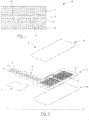
- Pre-loaded FSR 10 includes first and second substrates (membranes) 12, 14.
- Substrates 12, 14 may be individual portions obtained from the sheet of material such as, for example, Mylar.
- First substrate 12 includes electrically conductive traces 18 on an inner surface 20 of the first substrate.
- Second substrate 14 includes a resistive layer 22 on an inner surface 24 of the second substrate.
- Pre-loaded FSR 10 as shown in FIG. 1 has first substrate 12 positioned beneath second substrate 14 such that traces 18 are positioned beneath resistive layer 22.
- pre-loaded FSR 10 functions the same if first substrate 12 is positioned above second substrate 14 such that traces 18 are positioned above resistive layer 22.
- Traces 18 may be formed on first substrate 12 by any suitable means known in the art.
- traces 18 may be formed by depositing conductive material onto first substrate and then selectively removing portions of the conductive material to define the traces.
- Traces 18 may also be formed by depositing conductive polymer thick film ink (usually by screen printing) on first substrate 12.
- Dimensions for traces 18 depend on the dimensions of FSR 10, material and construction for substrates 12, 14, material and construction for resistive layer 22, and the like.
- Resistive layer 22 may be an FSR ink.
- First and second substrates 12, 14 are in contact with one another at all times such that resistive layer 22 of second substrate 14 contacts and electrically connects traces 18 of first substrate 12 together.
- This biasing force between substrates 12, 14 is present even in the absence of an externally applied force on at least one of the substrates.
- Resistive layer 22 shorts traces 18 together with an electrical resistance that inversely depends on the amount of the biasing force. As such, the electrical resistance between traces 18 decreases (increases) as the biasing force increases (decreases).
- the biasing force is constant such that the electrical resistance between traces 18 is constant in the absence of an externally applied force being applied to at least one of substrates 12, 14.
- Resistive layer 22 shorts traces together with an electrical resistance that inversely depends on the amount of the total force. As such, the electrical resistance between traces 18 decreases as the total force increases.
- pre-loaded FSR 10 includes second substrate 14 (i.e., top substrate), first substrate 12 (i.e., bottom substrate), and traces 18 on inner surface 20 of the first substrate.
- Pre-loaded FSR 10 further includes a rear adhesive layer 26 which adheres to the bottom side of bottom substrate 12.
- a top environmental protection layer on top of top substrate 14.
- the top protection layer could be transparent and have printing on its inside surface.
- Pre-loaded FSR 10 further includes a tail stiffener 28 for providing structural support to a connector portion 30 of bottom substrate 12. Tail stiffener 28 may provide additional thickness for meeting the specifications for insertion into a specific connector.
- Traces 18 are arranged within two zones. Multiple zones permit different functions such as locating the position of pressure on either substrate 12, 14, allowing independent pressure measurement in two locations, etc.
- the first zone is defined by a first set 32a of interdigitated trace fingers 18 and the second zone is defined by a second set 32b of interdigitated trace fingers 18.
- Each interdigitated trace finger set 32a, 32b shares a common trace 34.
- Interdigitated trace finger sets 32a, 32b has respective lead traces 36, 38.
- Common trace 34 and lead traces 36, 38 are electrically separated and extend down connector portion 30 of bottom substrate 12.
- FSR 40 is constructed in a usual fashion with bottom and top substrates 42, 44 separated by a spacer 46 at the outer perimeter.
- Bottom substrate 42 includes a set of interdigitated traces (not shown) on its inner surface and top substrate 44 includes a resistive layer (not shown) on its inner surface.
- Spacer 46 serves to space apart substrates 42, 44 and to adhere the structure together.
- actuator puck 48 and a surrounding adhesive shroud 50 are added in order to permanently pre-load FSR 40.
- the purpose of actuator puck 48 is to compress downward and close internal air gap 51 between substrates 42, 44. This happens when the FSR assembly and surrounding shroud are together laminated between two outer layers 52, 54 (see FIG. 5 ).
- Outer layers 52, 54 are components of a host device.
- one of outer layers 52 may be the front glass face of a cell phone and the second one of outer layers 54 may be an internal rigid frame such as around an LCD display.
- Shroud 50 supplies sufficient adhesive tension force to hold outer layers 52, 54 together and clamp FSR 40 closed (i.e., compress top substrate 44 towards bottom substrate 42 such that substrates 42, 44 contact and meet one another with a biasing force thereby resulting in FSR 40 being pre-loaded).
- Actuator puck 48 is a piece of material that may be screen printed onto the external surface of top substrate 48.
- actuator puck 48 may be screen printed using a dielectric spacer material such as Dupont 5018 UV cured screen-printable dielectric paste.
- actuator puck 48 may be die cut from an adhesive film such as 3M 7962.
- Actuator puck 48 may be die cut from a composite film such as 3M 7962 laminated to a polyester film. Any technique to form actuator puck 48 of sufficient thickness is acceptable.
- Shroud 50 may be formed and fabricated together with FSR 40 and supplied with the FSR as a single piece, or may be formed and assembled into the host device in separate steps from FSR 40.
- actuator puck 48 has to protrude above shroud 50 by a height greater than that of the air gap.
- this interference is large enough to guarantee loading of FSR 40 under all thickness tolerance scenarios but not thick enough to cause bowing of layer 54 or other problems of fit. This mechanical interference can be seen in FIG. 5 .
- the basis for detecting presses and releases (i.e., finger touches and releases) on a pre-loaded FSR includes measuring the time derivative of the electrical resistance of the pre-loaded FSR. That is, the basis for the measurement method is to measure the time derivative of the pre-loaded FSR output instead of the output itself. This works well because slow changes can be ignored while relatively fast changes caused by finger touches and releases are easily detected. It is noted that the biasing force will drift with temperature and/or aging of the mechanical FSR assembly over relatively long periods of time. These drifts are all on a much longer time scale than a finger contact press and release and can be ignored by the measurement method.
- Portable electronic devices such as cell phones often contain a microprocessor, microcontroller, or other integrated circuit having an analog-to-digital converter (ADC).
- ADC analog-to-digital converter
- such a system may be used to simply and easily measure the time derivative of the electrical resistance of a pre-loaded FSR and to detect presses and releases.
- a circuit 60 and algorithm which use the ADC (or an external ADC) for accomplishing this are described below.
- a circuit 60 that places a pre-loaded FSR into a voltage divider for measuring the time derivative of the electrical resistance of the pre-loaded FSR in order to detect presses and releases in accordance with an embodiment of the present invention is shown.
- the voltage to ADC 62 can be shown to have the largest change when R FSR and R 0 are equal, where R FSR is the resistance caused by an external force (i.e., finger touch or release) applied onto at least one of the substrates of the pre-loaded FSR and R 0 is the resistance caused by the pre-loaded biasing force. From a practical standpoint, it is only necessary that R FSR and R 0 have the same order of magnitude.
- Voltage at ADC 62 is measured on a regular schedule such as every 20ms (50 times per second). The regularity of this interval is important because changes in the time base could incorrectly appear as variations in dR/dt. Also, if dt is a constant then it can be ignored in further calculations.
- V ADC Vcc ⁇ R 0 / R 0 + R FSR
- V ADC is proportional to applied force. It is sufficient and useful to ignore any calibration or proportionality constants and simply equate the force at each time interval to V ADC .
- dF i F i - F i-1 , where i represents the ith sample and i-1 refers to the previous sample.
- a further step in the algorithm is to accumulate the dFi continuously into a sum. This amounts to a simple version of integrating over the derivative, which has the net effect of returning the force minus the force of the pre-load.
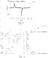
- FIGS. 7, 8 , and 9 respective example outputs 70, 80, and 90 produced by the measuring algorithm are shown.
- pre-loaded sensor 40 and shroud 50 are sandwiched between an aluminum plate 52 on the bottom and a 1mm thick plate of glass 54 on the top.
- FSR 40 is pre-loaded to a level around 20kOhms so R0 is chosen to be 20kOhms.
- the measurement period is 20ms (fifty samples per second).
- Each measurement is the sum of eight measurements taken in rapid succession with a 10-bit ADC.
- Outputs 70, 80, and 90 are shown in arbitrary units versus time.
- Output 80 shown in FIG. 8 is during a strong touch immediately followed by release of the touch. Again a positive peak 82 appears during press and a negative peak 84 during release. Peaks 82, 84 are roughly five times higher than peaks 72, 74 during a soft touch.
- Output 90 shown in FIG. 9 is during a light touch and a release where the touch and release are separated in time. The lingering between touch and release does not decrease the detectability of the release.
- touch detection can be accomplished with a simple thresholding scheme. For example, if dF/dt exceeds 200 units a touch is detected and the touch remains until dF/dt falls below -200 units.
- 200 units is only an example and depends on the specific mounting and measuring details of a given system.
- analog circuit 100 for use with the method of measuring a pre-loaded FSR in accordance with an embodiment of the present invention is shown.
- the use of analog circuit 100 is preferred, for example, when no ADC is present or when an ADC may not have the resources to measure the pre-loaded FSR on a regular schedule.
- Analog circuit 100 includes an analog op-amp circuit which is one approach to measuring a pre-loaded FSR.
- Analog circuit 100 shown in FIG. 10 is an example of such an analog op-amp circuit.
- Analog circuit 100 uses a single quad op-amp IC such as an MCP6144.
- One of the stages 102 provides a Vcc/2 reference
- one of the other stages 104 provides gain and smoothing
- two of the other stages 106, 108 are configured as comparators.
- R2 resistance of the FSR caused by an external applied force
- R1 resistance of the FSR caused by the constant biasing force
- the Vcc/2 reference voltage is created in stage 102 by a voltage divider and op amp U1C configured as a voltage follower.
- U1A of stage 104 which provides a gain of 100 and some low-pass smoothing.
- the inverting input of U1A is referenced to Vcc/2 so that its output while the FSR resistance is constant remains at Vcc/2 but its output while the FSR resistance is changing will swing all the way to either rail.
- the output of U1A is essentially the amplified derivative of the resistance signal. It swings high when R is dropping during a press and low when R2 is rising during a release.
- op-amp stage U1A The output of op-amp stage U1A is then fed into two comparators made from op amps (U1D and U1B) of stages 106, 108.
- Comparator U1D is configured to go high when its input signal is near ground.
- the other comparator U1B goes high when its input signal is near Vcc.
- the comparator outputs are two lines: "touch detected” and “release detected.” These could both be interfaced to a host CPU or combined using a latch to provide a single "currently touched” line.
- Example output 110 includes three oscilloscope trace outputs 112, 114, and 116 from analog circuit 100.
- Trace 112 is the output of U1A (point A in FIG. 10 ) during three touch and release events. Each touch has a positive peak 118 that clips at the positive power supply rail followed by a release event that creates a negative peak 120 that clips at the negative power supply rail.
- Traces 114, 116 are the respective outputs from the two comparators of stages 108, 106. While the derivative signal is near the positive rail, the "touch" comparator output 114 is high. While the derivative signal is near the negative rail the "release” signal 116 is high. A host device could detect these two lines and synthesize a "currently touched” signal using firmware.
Landscapes
- Engineering & Computer Science (AREA)
- Microelectronics & Electronic Packaging (AREA)
- Physics & Mathematics (AREA)
- General Physics & Mathematics (AREA)
- Force Measurement Appropriate To Specific Purposes (AREA)
Claims (10)
- Kraftmesswiderstandssystem, das Folgendes umfasst:einen Kraftmesswiderstand (FSR) (10; 40), der ein erstes Substrat (12; 42) enthält, das auf einer inneren Oberfläche (20) eine erste und eine zweite elektrisch leitende Spur (18) aufweist, wobei die Spuren voneinander elektrisch getrennt sind; undder FSR (10; 40) ferner ein zweites Substrat (14; 44) enthält, das auf einer inneren Oberfläche (24) eine Widerstandsschicht (22) aufweist;wobei die Substrate (12, 14) so angeordnet sind, dass sie ständig einer Vorbelastungskraft ausgesetzt sind, so dass die Substrate einander während der Vorbelastungskraft berühren, und wobei die Widerstandsschicht (22) die Spuren (18) berührt und elektrisch miteinander verbindet, um einen elektrischen Widerstand RBIAS zu erzeugen, der von der Vorbelastungskraft umgekehrt abhängig ist;wobei während eine äußere Kraft auf eines der Substrate in einer Richtung zu dem anderen Substrat ausgeübt wird, die Substrate (12, 14) einander mit einer Gesamtkraft berühren, die der Summe der Vorbelastungskraft und der äußeren Kraft entspricht, wobei die Widerstandsschicht (22) die Spuren (18) berührt und elektrisch miteinander verbindet, um einen elektrischen Gesamtwiderstand RFSR+RBIAS zu erzeugen, der von der Gesamtkraft umgekehrt abhängig ist;wobei die Vorbelastungskraft unabhängig entweder von der Anwesenheit oder Abwesenheit der äußeren Kraft vorhanden ist; undeine Analogschaltung (100), die mit den Spuren (18) verbunden ist und konfiguriert ist, eine Berührung auf dem FSR (10; 40) und eine Berührungsfreigabe von dem FSR (10; 40) zu detektieren, wobei die Analogschaltung (100) Folgendes umfasst:eine Stufe (102), die konfiguriert ist, eine erste Referenzspannung (Vcc) zu empfangen und eine zweite Referenzspannung (Vcc/2) bereitzustellen, wobei die zweite Referenzspannung (Vcc/2) in der Stufe (102) durch Teilen der ersten Referenzspannung (Vcc) mittels eines Spannungsteilers der Stufe (102) und mittels eines Operationsverstärkers (U1C) erzeugt wird, der in der Stufe (102) als ein Spannungsfolger konfiguriert ist;einen Spannungsteiler, der einen ersten Widerstand (R1) umfasst, der mit Masse verbunden ist und einen Widerstand einer äquivalenten Größenordnung wie RBIAS aufweist, und den FSR (10; 40) umfasst, wobei der FSR (10; 40) als ein zweiter Widerstand (R2) an einem ersten Knoten mit der ersten Referenzspannung (Vcc) und an einem zweiten Knoten mit dem ersten Widerstand (R1) verbunden ist, so dass Veränderungen in dem elektrischen Gesamtwiderstand RFSR+RBIAS, die durch die äußere Kraft verursacht werden, verursachen, dass die Spannung zwischen dem elektrischen Gesamtwiderstand RFSR+RBIAS und dem ersten Widerstand (R1) variiert;eine weitere Stufe (104), die Folgendes umfasst:einen Reihenkondensator (C1), der einen ersten Anschluss aufweist, der an dem zweiten Knoten mit dem Spannungsteiler verbunden ist;einen dritten Widerstand (R3), der einen ersten Anschluss, der mit einen zweiten Anschluss des Kondensators (C1) verbunden ist, und einen zweiten Anschluss aufweist, der an die zweiten Referenzspannung (Vcc/2) angeschlossen ist; und,einen invertierenden Verstärker (U1A), dessen nicht invertierender Eingang auch mit dem zweiten Anschluss des Kondensators (C1) verbunden ist und dessen invertierender Eingang sich auf die zweite Referenzspannung (Vcc/2) bezieht,so dass die Ausgabe des invertierenden Verstärkers (U1A) eine verstärkte Ableitung des FSR (10, 40) darstellt, die hoch schwingt, wenn der FSR (10, 40) während einer Berührung abfällt, und flach schwingt, wenn der FSR (10, 40) während einer Berührungsfreigabe ansteigt;einen ersten Komparator (108), der mit dem Ausgang des invertierenden Verstärkers (U1A) verbunden ist, und konfiguriert ist, ein erstes Signal (114) auszugeben, wobei das erste Signal einen hohen Wert aufweist, wenn eine Ausgabe (112) des invertierenden Verstärkers (U1A) größer ist als ein positiver Schwellenwert, der einer äußeren Kraftberührung auf dem FSR (10; 40) entspricht; undeinen zweiten Komparator (106), der auch mit dem Ausgang des invertierenden Verstärkers (U1A) verbunden ist und konfiguriert ist, ein zweites Signal (116) auszugeben, wobei das zweite Signal einen hohen Wert aufweist, wenn eine Ausgabe (112) der invertierenden Verstärkers (U1A) kleiner ist als ein negativer Schwellenwert, der einer äußeren Kraftberührungsfreigabe von dem FSR (10; 40) entspricht.
- FSR-System nach Anspruch 1, wobei:das erste Substrat (12; 42) auf der inneren Oberfläche eine dritte elektrisch leitende Spur enthält, wobei die Spuren voneinander elektrisch getrennt sind, wobei die erste und zweite Spur (32a) in einem ersten Bereich der inneren Oberfläche des ersten Substrats ineinander greifen und die zweite und die dritte Spur (32b) in einem anderen, zweiten Bereich der inneren Oberfläche des ersten Substrats ineinander greifen;wobei die Widerstandsschicht während der Vorbelastungskraft, die erste und die zweite Spur (32a) und die zweite und dritte Spur (32b) berührt und mit einem elektrischen Widerstand, der von der Vorbelastungskraft umgekehrt abhängig ist, elektrisch miteinander verbindet.
- FSR-System nach Anspruch 2, wobei:
während neben dem ersten Bereich eine erste äußere Kraft auf eines der Substrate in Richtung zu dem anderen Substrat ausgeübt wird, die Substrate einander in dem ersten Bereich mit einer ersten Gesamtkraft berühren, die der Summe der Vorbelastungskraft und der ersten äußeren Kraft entspricht, wobei die Widerstandsschicht die erste und zweite Spur berührt und mit einem elektrischen Widerstand, der von ersten Gesamtkraft umgekehrt abhängig ist, elektrisch miteinander verbindet. - FSR-System nach Anspruch 3, wobei:
während neben dem zweiten Bereich eine zweite äußere Kraft auf eines der Substrate in Richtung zu dem anderen Substrat ausgeübt wird, die Substrate einander in dem zweiten Bereich mit einer zweiten Gesamtkraft berühren, die der Summe der Vorbelastungskraft und der zweiten äußeren Kraft entspricht, wobei die Widerstandsschicht die zweite und dritte Spur berührt und mit einem elektrischen Widerstand, der von zweiten Gesamtkraft umgekehrt abhängig ist, elektrisch miteinander verbindet. - FSR-System nach Anspruch 1, wobei der FSR (40) ferner Folgendes umfasst:
eine Aktorscheibe (48), wobei die Aktorscheibe an einer äußeren Oberfläche eines der Substrate (42, 44) befestigt ist und die Substrate der Vorbelastungskraft aussetzt. - FSR-System nach Anspruch 5, wobei der FSR (40) ferner Folgendes umfasst:einen Abstandshalter (46), wobei der Abstandshalter die Substrate (42, 44) aneinander befestigt, so dass ein Luftspalt (51) die inneren Oberflächen der Substrate (42, 44) trennt;wobei die Aktorscheibe (48) die Substrate (42, 44) mit der Vorbelastungskraft zusammendrückt, so dass sich die inneren Oberflächen der Substrate (42, 44) miteinander in Kontakt befinden, wobei der Luftspalt (51) eliminiert wird.
- Verfahren zum Messen von Berührung und/oder Berührungsfreigabe, wobei das Verfahren Folgendes umfasst:Bereitstellen eines Kraftmesswiderstandssystems, das einen Kraftmesswiderstand (FSR) (10; 40) umfasst, der ein erstes und ein zweites Substrat (12, 42; 14, 44) aufweist, in dem das erste Substrat (12; 42) elektrisch leitende und voneinander getrennte Spuren (18) enthält und das zweite Substrat (14; 44) eine Widerstandsschicht (22) enthält, und in dem die Substrate angeordnet sind, so dass sie einer Vorbelastungskraft ständig ausgesetzt sind, so dass sich die Substrate (12, 42; 14, 44) miteinander in Kontakt befinden, wobei die Widerstandsschicht (22) die Spuren (18) berührt und elektrisch miteinander verbindet, um einen elektrischen Widerstand RBIAS zu erzeugen, der von der Vorbelastungskraft umgekehrt abhängig ist, wobei beim Ausüben einer äußeren Kraft auf eines der Substrate in einer Richtung zu dem anderen Substrat, die Substrate (12, 42; 14, 44) einander mit einer Gesamtkraft berühren, die der Summe der Vorbelastungskraft und der äußeren Kraft entspricht, wobei die Widerstandsschicht (22) die Spuren (18) berührt und elektrisch miteinander verbindet, um einen elektrischen Gesamtwiderstand RFSR+RBIAS zu erzeugen, der von der Gesamtkraft umgekehrt abhängig ist;Verbinden einer Analogschaltung (100) mit den Spuren (18) des FSR (10; 40), um eine Berührung auf dem FSR und eine Berührungsfreigabe von dem FSR zu detektieren, wobei die Analogschaltung (100) Folgendes umfasst:eine Stufe (102), die konfiguriert ist, eine erste Referenzspannung (Vcc) zu empfangen und eine zweite Referenzspannung (Vcc/2) bereitzustellen, wobei die zweite Referenzspannung (Vcc/2) in der Stufe (102) durch Teilen der ersten Referenzspannung (Vcc) mittels eines Spannungsteilers der Stufe (102) und mittels eines Operationsverstärkers (U1C) erzeugt wird, der in der Stufe (102) als ein Spannungsfolger konfiguriert ist;einen Spannungsteiler, der einen ersten Widerstand (R1) umfasst, der mit Masse verbunden ist und einen Widerstandswert einer äquivalenten Größenordnung wie RBIAS aufweist, und den FSR (10; 40) umfasst, wobei der FSR (10; 40) als ein zweiter Widerstand (R2) an einem ersten Knoten mit der ersten Referenzspannung (Vcc) und mit dem ersten Widerstand (R1) an einem zweiten Knoten verbunden ist, so dass Veränderungen in dem elektrischen Gesamtwiderstand RFSR+RBIAS, die durch die äußere Kraft verursacht werden, verursachen, dass die Spannung zwischen dem elektrischen Gesamtwiderstand RFSR+RBIAS und dem ersten Widerstand (R1) variiert;eine weitere Stufe (104), die Folgendes umfasst:einen Reihenkondensator (C1), der einen ersten Anschluss aufweist, der an dem zweiten Knoten mit dem Spannungsteiler verbunden ist;einen dritten Widerstand (R3), der einen ersten Anschluss, der mit einen zweiten Anschluss des Kondensators (C1) verbunden ist, und einen zweiten Anschluss aufweist, der an die zweiten Referenzspannung (Vcc/2) angeschlossen ist; undeinen invertierenden Verstärker (U1A), dessen nicht invertierender Eingang auch mit dem zweiten Anschluss des Kondensators (C1) verbunden ist, und dessen invertierender Eingang sich auf die zweite Referenzspannung (Vcc/2) bezieht,so dass die Ausgabe des invertierenden Verstärkers (U1A) eine verstärkte Ableitung des FSR (10, 40) darstellt, die hoch schwingt, wenn der FSR (10, 40) während einer Berührung abfällt, und flach schwingt, wenn der FSR (10, 40) während einer Berührungsfreigabe ansteigt;einen ersten Komparator (108), der mit dem Ausgang des invertierenden Verstärkers (U1A) verbunden ist, und konfiguriert ist, ein erstes Signal (114) auszugeben, wobei das erste Signal einen hohen Wert aufweist, wenn eine Ausgabe (112) des invertierenden Verstärkers (U1A) größer ist als ein positiver Schwellenwert, der einer äußeren Kraftberührung auf dem FSR (10; 40) entspricht; undeinen zweiten Komparator (106), der auch mit dem Ausgang des invertierenden Verstärkers (U1A) verbunden ist und konfiguriert ist, ein zweites Signal (116) auszugeben, wobei das zweite Signal einen hohen Wert aufweist, wenn eine Ausgabe (112) der invertierenden Verstärkers (U1A) kleiner ist als ein negativer Schwellenwert, der einer äußeren Kraftberührungsfreigabe von dem FSR (10; 40) entspricht;Detektieren einer Berührung auf dem FSR als Reaktion auf das erste Signal (114); undDetektieren einer Freigabe einer Berührung von dem FSR als Reaktion auf das zweite Signal (116).
- Verfahren nach Anspruch 7, wobei:die Spannungsausgabe von dem Spannungsteiler zu einem bestimmten Zeitpunkt umgekehrt proportional zu dem elektrischen Gesamtwiderstand RFSR+RBIAS zu dem bestimmten Zeitpunkt ist.
- Verfahren nach Anspruch 7, das ferner Folgendes umfasst:
Auswählen der Vorbelastungskraft derart, dass der elektrische Widerstand RBIAS zwischen den Spuren, als ein Ergebnis der Vorbelastungskraft, dieselbe Größenordnung aufweist wie der elektrische Widerstand RFSR zwischen den Spuren, als ein Ergebnis einer ursprünglichen Komponente einer äußeren Kraft, die auf eines der Substrate in einer Richtung zu dem anderen Substrat ausgeübt wird, ohne den Effekt der Vorbelastungskraft auf den elektrischen Widerstand RBIAS. - Verfahren nach Anspruch 7, wobei das Verfahren ferner Folgendes umfasst:
Auswählen von RBIAS derart, dass RBIAS dieselbe Größenordnung aufweist, wie RFSR zu dem Zeitpunkt, an dem eine ursprünglichen Komponente einer äußeren Kraft auf eines der Substrate in einer Richtung zu dem anderen Substrat ausgeübt wird.
Applications Claiming Priority (2)
| Application Number | Priority Date | Filing Date | Title |
|---|---|---|---|
| US11/986,873 US7772960B2 (en) | 2007-11-27 | 2007-11-27 | Pre-loaded force sensing resistor and method |
| PCT/US2008/084346 WO2009070503A1 (en) | 2007-11-27 | 2008-11-21 | Pre-load force sensing resistor and method |
Publications (3)
| Publication Number | Publication Date |
|---|---|
| EP2215541A1 EP2215541A1 (de) | 2010-08-11 |
| EP2215541A4 EP2215541A4 (de) | 2018-03-21 |
| EP2215541B1 true EP2215541B1 (de) | 2020-05-06 |
Family
ID=40669189
Family Applications (1)
| Application Number | Title | Priority Date | Filing Date |
|---|---|---|---|
| EP08853471.4A Active EP2215541B1 (de) | 2007-11-27 | 2008-11-21 | Vorgeladener krafterfassungswiderstand und entsprechendes verfahren |
Country Status (3)
| Country | Link |
|---|---|
| US (1) | US7772960B2 (de) |
| EP (1) | EP2215541B1 (de) |
| WO (1) | WO2009070503A1 (de) |
Families Citing this family (47)
| Publication number | Priority date | Publication date | Assignee | Title |
|---|---|---|---|---|
| JP5304544B2 (ja) * | 2009-08-28 | 2013-10-02 | ソニー株式会社 | 情報処理装置、情報処理方法、及びプログラム |
| WO2011047171A2 (en) | 2009-10-16 | 2011-04-21 | Kesumo, Llc | Foot-operated controller |
| US8368505B2 (en) * | 2010-03-12 | 2013-02-05 | Almax Manufacturing Corporation | Switch using variable resistance layer to control state |
| DE102011006344B4 (de) | 2010-03-31 | 2020-03-12 | Joyson Safety Systems Acquisition Llc | Insassenmesssystem |
| JP5805974B2 (ja) | 2010-03-31 | 2015-11-10 | ティーケー ホールディングス,インコーポレーテッド | ステアリングホイールセンサ |
| US8983732B2 (en) | 2010-04-02 | 2015-03-17 | Tk Holdings Inc. | Steering wheel with hand pressure sensing |
| JP5759230B2 (ja) | 2010-04-02 | 2015-08-05 | ティーケー ホールディングス,インコーポレーテッド | 手センサを有するステアリング・ホイール |
| CN102959375B (zh) | 2010-07-07 | 2015-07-22 | 德尔菲技术公司 | 用于检测按钮的激活的算法 |
| EP2413120A1 (de) | 2010-07-30 | 2012-02-01 | Delphi Technologies, Inc. | Druckempfindliche Wandleranordnung und Ansteuerungsverfahren für ein System mit einer derartigen Anordnung |
| FR2963838B1 (fr) | 2010-08-12 | 2012-07-27 | Delphi Tech Inc | Panneau de commande a touches resistives et capteurs precontraints |
| FR2963839B1 (fr) * | 2010-08-13 | 2012-08-17 | Delphi Tech Inc | Panneau de commande comportant une touche resistive |
| US8724038B2 (en) | 2010-10-18 | 2014-05-13 | Qualcomm Mems Technologies, Inc. | Wraparound assembly for combination touch, handwriting and fingerprint sensor |
| FR2973129B1 (fr) * | 2011-03-21 | 2013-03-29 | Delphi Tech Inc | Panneau de commande a touches resistives |
| JP5750296B2 (ja) * | 2011-04-15 | 2015-07-15 | アルパイン株式会社 | 車載用ディスプレイ装置 |
| FR2976867B1 (fr) | 2011-06-23 | 2013-11-08 | Delphi Tech Inc | Panneau de commande comportant une touche retro-eclairee de type resistive |
| EP2583586B2 (de) * | 2011-10-18 | 2021-08-04 | Kesseböhmer Produktions GmbH & Co. KG | Vorrichtung zur Erfassung von Kollisionen und entsprechendes Verfahren |
| US9352456B2 (en) | 2011-10-26 | 2016-05-31 | Black & Decker Inc. | Power tool with force sensing electronic clutch |
| JP5895615B2 (ja) * | 2012-03-09 | 2016-03-30 | セイコーエプソン株式会社 | センサーモジュール、力検出装置及びロボット |
| US9076419B2 (en) | 2012-03-14 | 2015-07-07 | Bebop Sensors, Inc. | Multi-touch pad controller |
| WO2013154720A1 (en) | 2012-04-13 | 2013-10-17 | Tk Holdings Inc. | Pressure sensor including a pressure sensitive material for use with control systems and methods of using the same |
| US9024910B2 (en) | 2012-04-23 | 2015-05-05 | Qualcomm Mems Technologies, Inc. | Touchscreen with bridged force-sensitive resistors |
| WO2014043664A1 (en) | 2012-09-17 | 2014-03-20 | Tk Holdings Inc. | Single layer force sensor |
| TWI629459B (zh) * | 2013-02-06 | 2018-07-11 | 藤倉股份有限公司 | Method for manufacturing pressure detecting device, pressure detecting device, pressure detecting device and electronic device |
| DE102013101835A1 (de) * | 2013-02-25 | 2014-08-28 | Haake Technik Gmbh | Zweikanaliger, mehrlagiger taktiler Sensor |
| US20150199048A1 (en) * | 2014-01-15 | 2015-07-16 | Carestream Health, Inc. | Touch panel assembly |
| US9753568B2 (en) * | 2014-05-15 | 2017-09-05 | Bebop Sensors, Inc. | Flexible sensors and applications |
| US10362989B2 (en) | 2014-06-09 | 2019-07-30 | Bebop Sensors, Inc. | Sensor system integrated with a glove |
| JP6129424B2 (ja) * | 2014-08-26 | 2017-05-17 | 深▲せん▼紐迪瑞科技開発有限公司Shenzhen New Degree Technology Co.,Ltd. | 分離式圧力センサ及び電子装置 |
| US9863823B2 (en) | 2015-02-27 | 2018-01-09 | Bebop Sensors, Inc. | Sensor systems integrated with footwear |
| US9827996B2 (en) | 2015-06-25 | 2017-11-28 | Bebop Sensors, Inc. | Sensor systems integrated with steering wheels |
| KR102092864B1 (ko) | 2015-08-31 | 2020-03-24 | 삼성전자주식회사 | 센서 모듈 및 이를 포함하는 운동 보조 장치 |
| US10765402B2 (en) * | 2015-11-23 | 2020-09-08 | QT Ultrasound LLC | Automatic laterality identification for ultrasound tomography systems |
| US10118696B1 (en) | 2016-03-31 | 2018-11-06 | Steven M. Hoffberg | Steerable rotating projectile |
| US10838246B2 (en) | 2016-09-29 | 2020-11-17 | Intel Corporation | Force-sensitive display assembly for user input |
| JP2018077191A (ja) * | 2016-11-11 | 2018-05-17 | 北川工業株式会社 | 感圧センサー |
| JP6770743B2 (ja) | 2016-12-20 | 2020-10-21 | 北川工業株式会社 | 感圧センサー |
| ES2674339B1 (es) * | 2016-12-28 | 2019-04-02 | Macsha Emea S L | Dispositivo sensor para competiciones de natacion o similares |
| GB201705751D0 (en) * | 2017-04-10 | 2017-05-24 | Rainbow Tech Systems Ltd | Force sensitive resistor |
| JP6566182B1 (ja) * | 2017-10-03 | 2019-08-28 | 株式会社村田製作所 | 押圧センサ及び電子機器 |
| US11712637B1 (en) | 2018-03-23 | 2023-08-01 | Steven M. Hoffberg | Steerable disk or ball |
| US10884496B2 (en) | 2018-07-05 | 2021-01-05 | Bebop Sensors, Inc. | One-size-fits-all data glove |
| WO2020061592A1 (en) * | 2018-09-21 | 2020-03-26 | Carnegie Mellon University | Force sensor |
| US11480481B2 (en) | 2019-03-13 | 2022-10-25 | Bebop Sensors, Inc. | Alignment mechanisms sensor systems employing piezoresistive materials |
| KR102677514B1 (ko) | 2019-05-22 | 2024-06-21 | 삼성전자주식회사 | 압력 측정 장치 |
| SE546404C2 (en) * | 2019-10-21 | 2024-10-29 | Marshall Group AB | In-ear audio listening device comprising a user input element |
| WO2021102295A1 (en) * | 2019-11-21 | 2021-05-27 | Thomas Baer | Systems and methods for detecting running and walking strides and foot strikes |
| WO2025144547A1 (en) * | 2023-12-29 | 2025-07-03 | Dexcom, Inc. | Compression event detection and prevention |
Family Cites Families (11)
| Publication number | Priority date | Publication date | Assignee | Title |
|---|---|---|---|---|
| US4051540A (en) * | 1976-04-20 | 1977-09-27 | Dictaphone Corporation | Instruction indicating apparatus for a record and/or playback device |
| US4314228A (en) | 1980-04-16 | 1982-02-02 | Eventoff Franklin Neal | Pressure transducer |
| US4314227A (en) | 1979-09-24 | 1982-02-02 | Eventoff Franklin Neal | Electronic pressure sensitive transducer apparatus |
| US4489302A (en) | 1979-09-24 | 1984-12-18 | Eventoff Franklin Neal | Electronic pressure sensitive force transducer |
| FR2632069B1 (fr) | 1988-05-30 | 1990-12-14 | Garcia Manuel | Capteur de detection par vitesse de variation d'impedance ou par variation d'impedance |
| US5440237A (en) | 1993-06-01 | 1995-08-08 | Incontrol Solutions, Inc. | Electronic force sensing with sensor normalization |
| US5515040A (en) * | 1993-09-28 | 1996-05-07 | Sejin Electron, Incorporated | Methods of self-calibration for a key-type mouse |
| DE50007780D1 (de) | 2000-05-17 | 2004-10-21 | Infineon Technologies Ag | Schaltungsanordnung zur Detektion einer Funktionsstörung |
| JP3986985B2 (ja) * | 2003-03-25 | 2007-10-03 | 株式会社デンソー | 感圧抵抗体及び感圧センサ |
| US7113179B2 (en) | 2004-06-23 | 2006-09-26 | Interlink Electronics, Inc. | Force sensing resistor with calibration element and method of manufacturing same |
| US7528337B2 (en) * | 2007-05-15 | 2009-05-05 | Panasonic Corporation | Pressure sensitive conductive sheet and panel switch using same |
-
2007
- 2007-11-27 US US11/986,873 patent/US7772960B2/en active Active
-
2008
- 2008-11-21 EP EP08853471.4A patent/EP2215541B1/de active Active
- 2008-11-21 WO PCT/US2008/084346 patent/WO2009070503A1/en not_active Ceased
Non-Patent Citations (1)
| Title |
|---|
| None * |
Also Published As
| Publication number | Publication date |
|---|---|
| US7772960B2 (en) | 2010-08-10 |
| EP2215541A4 (de) | 2018-03-21 |
| WO2009070503A1 (en) | 2009-06-04 |
| US20090134966A1 (en) | 2009-05-28 |
| EP2215541A1 (de) | 2010-08-11 |
Similar Documents
| Publication | Publication Date | Title |
|---|---|---|
| EP2215541B1 (de) | Vorgeladener krafterfassungswiderstand und entsprechendes verfahren | |
| US10353506B2 (en) | Dual resistive strain and pressure sensor for force touch | |
| CN110192172B (zh) | 压力感应式结构及电子产品 | |
| KR101597861B1 (ko) | 센서, 센서를 포함하는 디스플레이, 및 센서를 사용하는 방법 | |
| JP5586776B1 (ja) | 入力装置及び入力装置の制御方法 | |
| CN108089736B (zh) | 用于感测用户输入的设备 | |
| EP2287716B1 (de) | Verfahren zur Erkennung einer Position einer Berührung auf einem berührungsempfindlichen Element und elektronische Vorrichtung damit | |
| EP2546730A2 (de) | Kombinierte Kraft- und Näherungsmessung | |
| CN105556436A (zh) | 电子设备以及电子设备的控制方法 | |
| JPS59216237A (ja) | デ−タ入力装置 | |
| EP2278441A3 (de) | Verfahren zum Erfassen einer Position auf einer Berührungsvorrichtung | |
| US20100077868A1 (en) | Tactile sensor | |
| CN111998976B (zh) | 压力传感器和电子设备 | |
| TWI547841B (zh) | And a method of manufacturing the input device and the input device | |
| CN105849677A (zh) | 电子设备以及电子设备的控制方法 | |
| US11913846B2 (en) | Force sensing systems | |
| US9933867B2 (en) | Active pen capacitive displacement gauge | |
| CN107346188B (zh) | 压力感应模组、终端、图像显示方法及装置 | |
| CN215120758U (zh) | 感应装置和电子产品 | |
| CN115439895B (zh) | 指纹压感模组及电子设备 | |
| CN110858108A (zh) | 一种压力感测模组、触控面板以及触控面板两点触摸压力检测方法 | |
| CN212322228U (zh) | 触摸面板 | |
| CN113242965B (zh) | 压力传感器及电子终端 | |
| CN109186819B (zh) | 一种mems压力传感器模组 | |
| CN218156598U (zh) | 一种惠斯通电桥压力检测元件及电子设备 |
Legal Events
| Date | Code | Title | Description |
|---|---|---|---|
| PUAI | Public reference made under article 153(3) epc to a published international application that has entered the european phase |
Free format text: ORIGINAL CODE: 0009012 |
|
| 17P | Request for examination filed |
Effective date: 20100317 |
|
| AK | Designated contracting states |
Kind code of ref document: A1 Designated state(s): AT BE BG CH CY CZ DE DK EE ES FI FR GB GR HR HU IE IS IT LI LT LU LV MC MT NL NO PL PT RO SE SI SK TR |
|
| AX | Request for extension of the european patent |
Extension state: AL BA MK RS |
|
| DAX | Request for extension of the european patent (deleted) | ||
| RA4 | Supplementary search report drawn up and despatched (corrected) |
Effective date: 20180220 |
|
| RIC1 | Information provided on ipc code assigned before grant |
Ipc: G06F 3/045 20060101AFI20180214BHEP |
|
| STAA | Information on the status of an ep patent application or granted ep patent |
Free format text: STATUS: EXAMINATION IS IN PROGRESS |
|
| 17Q | First examination report despatched |
Effective date: 20190328 |
|
| GRAP | Despatch of communication of intention to grant a patent |
Free format text: ORIGINAL CODE: EPIDOSNIGR1 |
|
| STAA | Information on the status of an ep patent application or granted ep patent |
Free format text: STATUS: GRANT OF PATENT IS INTENDED |
|
| INTG | Intention to grant announced |
Effective date: 20191029 |
|
| GRAS | Grant fee paid |
Free format text: ORIGINAL CODE: EPIDOSNIGR3 |
|
| GRAJ | Information related to disapproval of communication of intention to grant by the applicant or resumption of examination proceedings by the epo deleted |
Free format text: ORIGINAL CODE: EPIDOSDIGR1 |
|
| GRAL | Information related to payment of fee for publishing/printing deleted |
Free format text: ORIGINAL CODE: EPIDOSDIGR3 |
|
| STAA | Information on the status of an ep patent application or granted ep patent |
Free format text: STATUS: EXAMINATION IS IN PROGRESS |
|
| GRAR | Information related to intention to grant a patent recorded |
Free format text: ORIGINAL CODE: EPIDOSNIGR71 |
|
| STAA | Information on the status of an ep patent application or granted ep patent |
Free format text: STATUS: GRANT OF PATENT IS INTENDED |
|
| GRAA | (expected) grant |
Free format text: ORIGINAL CODE: 0009210 |
|
| STAA | Information on the status of an ep patent application or granted ep patent |
Free format text: STATUS: THE PATENT HAS BEEN GRANTED |
|
| INTC | Intention to grant announced (deleted) | ||
| AK | Designated contracting states |
Kind code of ref document: B1 Designated state(s): AT BE BG CH CY CZ DE DK EE ES FI FR GB GR HR HU IE IS IT LI LT LU LV MC MT NL NO PL PT RO SE SI SK TR |
|
| INTG | Intention to grant announced |
Effective date: 20200331 |
|
| REG | Reference to a national code |
Ref country code: GB Ref legal event code: FG4D |
|
| REG | Reference to a national code |
Ref country code: CH Ref legal event code: EP Ref country code: AT Ref legal event code: REF Ref document number: 1267846 Country of ref document: AT Kind code of ref document: T Effective date: 20200515 |
|
| REG | Reference to a national code |
Ref country code: IE Ref legal event code: FG4D |
|
| REG | Reference to a national code |
Ref country code: DE Ref legal event code: R096 Ref document number: 602008062664 Country of ref document: DE |
|
| REG | Reference to a national code |
Ref country code: LT Ref legal event code: MG4D |
|
| REG | Reference to a national code |
Ref country code: NL Ref legal event code: MP Effective date: 20200506 |
|
| PG25 | Lapsed in a contracting state [announced via postgrant information from national office to epo] |
Ref country code: SE Free format text: LAPSE BECAUSE OF FAILURE TO SUBMIT A TRANSLATION OF THE DESCRIPTION OR TO PAY THE FEE WITHIN THE PRESCRIBED TIME-LIMIT Effective date: 20200506 Ref country code: LT Free format text: LAPSE BECAUSE OF FAILURE TO SUBMIT A TRANSLATION OF THE DESCRIPTION OR TO PAY THE FEE WITHIN THE PRESCRIBED TIME-LIMIT Effective date: 20200506 Ref country code: NO Free format text: LAPSE BECAUSE OF FAILURE TO SUBMIT A TRANSLATION OF THE DESCRIPTION OR TO PAY THE FEE WITHIN THE PRESCRIBED TIME-LIMIT Effective date: 20200806 Ref country code: GR Free format text: LAPSE BECAUSE OF FAILURE TO SUBMIT A TRANSLATION OF THE DESCRIPTION OR TO PAY THE FEE WITHIN THE PRESCRIBED TIME-LIMIT Effective date: 20200807 Ref country code: FI Free format text: LAPSE BECAUSE OF FAILURE TO SUBMIT A TRANSLATION OF THE DESCRIPTION OR TO PAY THE FEE WITHIN THE PRESCRIBED TIME-LIMIT Effective date: 20200506 Ref country code: IS Free format text: LAPSE BECAUSE OF FAILURE TO SUBMIT A TRANSLATION OF THE DESCRIPTION OR TO PAY THE FEE WITHIN THE PRESCRIBED TIME-LIMIT Effective date: 20200906 Ref country code: PT Free format text: LAPSE BECAUSE OF FAILURE TO SUBMIT A TRANSLATION OF THE DESCRIPTION OR TO PAY THE FEE WITHIN THE PRESCRIBED TIME-LIMIT Effective date: 20200907 |
|
| PG25 | Lapsed in a contracting state [announced via postgrant information from national office to epo] |
Ref country code: LV Free format text: LAPSE BECAUSE OF FAILURE TO SUBMIT A TRANSLATION OF THE DESCRIPTION OR TO PAY THE FEE WITHIN THE PRESCRIBED TIME-LIMIT Effective date: 20200506 Ref country code: HR Free format text: LAPSE BECAUSE OF FAILURE TO SUBMIT A TRANSLATION OF THE DESCRIPTION OR TO PAY THE FEE WITHIN THE PRESCRIBED TIME-LIMIT Effective date: 20200506 Ref country code: BG Free format text: LAPSE BECAUSE OF FAILURE TO SUBMIT A TRANSLATION OF THE DESCRIPTION OR TO PAY THE FEE WITHIN THE PRESCRIBED TIME-LIMIT Effective date: 20200806 |
|
| REG | Reference to a national code |
Ref country code: AT Ref legal event code: MK05 Ref document number: 1267846 Country of ref document: AT Kind code of ref document: T Effective date: 20200506 |
|
| PG25 | Lapsed in a contracting state [announced via postgrant information from national office to epo] |
Ref country code: NL Free format text: LAPSE BECAUSE OF FAILURE TO SUBMIT A TRANSLATION OF THE DESCRIPTION OR TO PAY THE FEE WITHIN THE PRESCRIBED TIME-LIMIT Effective date: 20200506 |
|
| PG25 | Lapsed in a contracting state [announced via postgrant information from national office to epo] |
Ref country code: RO Free format text: LAPSE BECAUSE OF FAILURE TO SUBMIT A TRANSLATION OF THE DESCRIPTION OR TO PAY THE FEE WITHIN THE PRESCRIBED TIME-LIMIT Effective date: 20200506 Ref country code: CZ Free format text: LAPSE BECAUSE OF FAILURE TO SUBMIT A TRANSLATION OF THE DESCRIPTION OR TO PAY THE FEE WITHIN THE PRESCRIBED TIME-LIMIT Effective date: 20200506 Ref country code: ES Free format text: LAPSE BECAUSE OF FAILURE TO SUBMIT A TRANSLATION OF THE DESCRIPTION OR TO PAY THE FEE WITHIN THE PRESCRIBED TIME-LIMIT Effective date: 20200506 Ref country code: AT Free format text: LAPSE BECAUSE OF FAILURE TO SUBMIT A TRANSLATION OF THE DESCRIPTION OR TO PAY THE FEE WITHIN THE PRESCRIBED TIME-LIMIT Effective date: 20200506 Ref country code: EE Free format text: LAPSE BECAUSE OF FAILURE TO SUBMIT A TRANSLATION OF THE DESCRIPTION OR TO PAY THE FEE WITHIN THE PRESCRIBED TIME-LIMIT Effective date: 20200506 Ref country code: IT Free format text: LAPSE BECAUSE OF FAILURE TO SUBMIT A TRANSLATION OF THE DESCRIPTION OR TO PAY THE FEE WITHIN THE PRESCRIBED TIME-LIMIT Effective date: 20200506 Ref country code: DK Free format text: LAPSE BECAUSE OF FAILURE TO SUBMIT A TRANSLATION OF THE DESCRIPTION OR TO PAY THE FEE WITHIN THE PRESCRIBED TIME-LIMIT Effective date: 20200506 |
|
| PGFP | Annual fee paid to national office [announced via postgrant information from national office to epo] |
Ref country code: FR Payment date: 20201119 Year of fee payment: 13 Ref country code: DE Payment date: 20201118 Year of fee payment: 13 |
|
| REG | Reference to a national code |
Ref country code: DE Ref legal event code: R097 Ref document number: 602008062664 Country of ref document: DE |
|
| PG25 | Lapsed in a contracting state [announced via postgrant information from national office to epo] |
Ref country code: SK Free format text: LAPSE BECAUSE OF FAILURE TO SUBMIT A TRANSLATION OF THE DESCRIPTION OR TO PAY THE FEE WITHIN THE PRESCRIBED TIME-LIMIT Effective date: 20200506 Ref country code: PL Free format text: LAPSE BECAUSE OF FAILURE TO SUBMIT A TRANSLATION OF THE DESCRIPTION OR TO PAY THE FEE WITHIN THE PRESCRIBED TIME-LIMIT Effective date: 20200506 |
|
| PLBE | No opposition filed within time limit |
Free format text: ORIGINAL CODE: 0009261 |
|
| STAA | Information on the status of an ep patent application or granted ep patent |
Free format text: STATUS: NO OPPOSITION FILED WITHIN TIME LIMIT |
|
| 26N | No opposition filed |
Effective date: 20210209 |
|
| PG25 | Lapsed in a contracting state [announced via postgrant information from national office to epo] |
Ref country code: SI Free format text: LAPSE BECAUSE OF FAILURE TO SUBMIT A TRANSLATION OF THE DESCRIPTION OR TO PAY THE FEE WITHIN THE PRESCRIBED TIME-LIMIT Effective date: 20200506 |
|
| PG25 | Lapsed in a contracting state [announced via postgrant information from national office to epo] |
Ref country code: MC Free format text: LAPSE BECAUSE OF FAILURE TO SUBMIT A TRANSLATION OF THE DESCRIPTION OR TO PAY THE FEE WITHIN THE PRESCRIBED TIME-LIMIT Effective date: 20200506 |
|
| REG | Reference to a national code |
Ref country code: CH Ref legal event code: PL |
|
| PG25 | Lapsed in a contracting state [announced via postgrant information from national office to epo] |
Ref country code: LU Free format text: LAPSE BECAUSE OF NON-PAYMENT OF DUE FEES Effective date: 20201121 |
|
| REG | Reference to a national code |
Ref country code: BE Ref legal event code: MM Effective date: 20201130 |
|
| PG25 | Lapsed in a contracting state [announced via postgrant information from national office to epo] |
Ref country code: CH Free format text: LAPSE BECAUSE OF NON-PAYMENT OF DUE FEES Effective date: 20201130 Ref country code: LI Free format text: LAPSE BECAUSE OF NON-PAYMENT OF DUE FEES Effective date: 20201130 |
|
| PG25 | Lapsed in a contracting state [announced via postgrant information from national office to epo] |
Ref country code: IE Free format text: LAPSE BECAUSE OF NON-PAYMENT OF DUE FEES Effective date: 20201121 |
|
| PG25 | Lapsed in a contracting state [announced via postgrant information from national office to epo] |
Ref country code: TR Free format text: LAPSE BECAUSE OF FAILURE TO SUBMIT A TRANSLATION OF THE DESCRIPTION OR TO PAY THE FEE WITHIN THE PRESCRIBED TIME-LIMIT Effective date: 20200506 Ref country code: MT Free format text: LAPSE BECAUSE OF FAILURE TO SUBMIT A TRANSLATION OF THE DESCRIPTION OR TO PAY THE FEE WITHIN THE PRESCRIBED TIME-LIMIT Effective date: 20200506 Ref country code: CY Free format text: LAPSE BECAUSE OF FAILURE TO SUBMIT A TRANSLATION OF THE DESCRIPTION OR TO PAY THE FEE WITHIN THE PRESCRIBED TIME-LIMIT Effective date: 20200506 |
|
| REG | Reference to a national code |
Ref country code: DE Ref legal event code: R119 Ref document number: 602008062664 Country of ref document: DE |
|
| PG25 | Lapsed in a contracting state [announced via postgrant information from national office to epo] |
Ref country code: BE Free format text: LAPSE BECAUSE OF NON-PAYMENT OF DUE FEES Effective date: 20201130 |
|
| PG25 | Lapsed in a contracting state [announced via postgrant information from national office to epo] |
Ref country code: DE Free format text: LAPSE BECAUSE OF NON-PAYMENT OF DUE FEES Effective date: 20220601 |
|
| PG25 | Lapsed in a contracting state [announced via postgrant information from national office to epo] |
Ref country code: FR Free format text: LAPSE BECAUSE OF NON-PAYMENT OF DUE FEES Effective date: 20211130 |
|
| P01 | Opt-out of the competence of the unified patent court (upc) registered |
Effective date: 20230528 |
|
| PGFP | Annual fee paid to national office [announced via postgrant information from national office to epo] |
Ref country code: GB Payment date: 20251110 Year of fee payment: 18 |