EP2216663B1 - Struktur und Verfahren zur Justierung einer optischen Faser mit einem sub-mikronischen Lichtwellenleiter - Google Patents
Struktur und Verfahren zur Justierung einer optischen Faser mit einem sub-mikronischen Lichtwellenleiter Download PDFInfo
- Publication number
- EP2216663B1 EP2216663B1 EP10152313A EP10152313A EP2216663B1 EP 2216663 B1 EP2216663 B1 EP 2216663B1 EP 10152313 A EP10152313 A EP 10152313A EP 10152313 A EP10152313 A EP 10152313A EP 2216663 B1 EP2216663 B1 EP 2216663B1
- Authority
- EP
- European Patent Office
- Prior art keywords
- optical
- waveguide
- upper layer
- optical fiber
- core
- Prior art date
- Legal status (The legal status is an assumption and is not a legal conclusion. Google has not performed a legal analysis and makes no representation as to the accuracy of the status listed.)
- Not-in-force
Links
- 230000003287 optical effect Effects 0.000 title claims abstract description 71
- 239000013307 optical fiber Substances 0.000 title claims abstract description 61
- 238000000034 method Methods 0.000 title claims abstract description 29
- 239000003292 glue Substances 0.000 claims abstract description 22
- 238000000605 extraction Methods 0.000 claims abstract description 9
- 230000008878 coupling Effects 0.000 claims description 18
- 238000010168 coupling process Methods 0.000 claims description 18
- 238000005859 coupling reaction Methods 0.000 claims description 18
- 238000005253 cladding Methods 0.000 claims description 12
- 229910052710 silicon Inorganic materials 0.000 claims description 11
- 239000010703 silicon Substances 0.000 claims description 11
- VYPSYNLAJGMNEJ-UHFFFAOYSA-N Silicium dioxide Chemical compound O=[Si]=O VYPSYNLAJGMNEJ-UHFFFAOYSA-N 0.000 claims description 10
- 229910052814 silicon oxide Inorganic materials 0.000 claims description 10
- 230000000149 penetrating effect Effects 0.000 claims description 3
- 238000000151 deposition Methods 0.000 claims description 2
- 239000000835 fiber Substances 0.000 abstract description 10
- XUIMIQQOPSSXEZ-UHFFFAOYSA-N Silicon Chemical compound [Si] XUIMIQQOPSSXEZ-UHFFFAOYSA-N 0.000 description 9
- 239000000853 adhesive Substances 0.000 description 7
- 230000001070 adhesive effect Effects 0.000 description 7
- 239000000463 material Substances 0.000 description 4
- 230000005540 biological transmission Effects 0.000 description 3
- 239000000758 substrate Substances 0.000 description 3
- 230000008901 benefit Effects 0.000 description 2
- NIXOWILDQLNWCW-UHFFFAOYSA-M Acrylate Chemical compound [O-]C(=O)C=C NIXOWILDQLNWCW-UHFFFAOYSA-M 0.000 description 1
- 239000004593 Epoxy Substances 0.000 description 1
- 238000009825 accumulation Methods 0.000 description 1
- 230000003321 amplification Effects 0.000 description 1
- 230000000593 degrading effect Effects 0.000 description 1
- 238000001914 filtration Methods 0.000 description 1
- 238000005286 illumination Methods 0.000 description 1
- 239000012212 insulator Substances 0.000 description 1
- 230000010354 integration Effects 0.000 description 1
- 239000002184 metal Substances 0.000 description 1
- 238000004377 microelectronic Methods 0.000 description 1
- 238000012986 modification Methods 0.000 description 1
- 230000004048 modification Effects 0.000 description 1
- 230000003472 neutralizing effect Effects 0.000 description 1
- 238000003199 nucleic acid amplification method Methods 0.000 description 1
- 230000005693 optoelectronics Effects 0.000 description 1
- 230000010287 polarization Effects 0.000 description 1
- 229920001296 polysiloxane Polymers 0.000 description 1
- 230000008569 process Effects 0.000 description 1
- 230000000750 progressive effect Effects 0.000 description 1
- 239000004065 semiconductor Substances 0.000 description 1
- LIVNPJMFVYWSIS-UHFFFAOYSA-N silicon monoxide Chemical compound [Si-]#[O+] LIVNPJMFVYWSIS-UHFFFAOYSA-N 0.000 description 1
- 230000003595 spectral effect Effects 0.000 description 1
- 235000012431 wafers Nutrition 0.000 description 1
Images


Classifications
-
- G—PHYSICS
- G02—OPTICS
- G02B—OPTICAL ELEMENTS, SYSTEMS OR APPARATUS
- G02B6/00—Light guides; Structural details of arrangements comprising light guides and other optical elements, e.g. couplings
- G02B6/24—Coupling light guides
- G02B6/26—Optical coupling means
- G02B6/34—Optical coupling means utilising prism or grating
-
- G—PHYSICS
- G02—OPTICS
- G02B—OPTICAL ELEMENTS, SYSTEMS OR APPARATUS
- G02B6/00—Light guides; Structural details of arrangements comprising light guides and other optical elements, e.g. couplings
- G02B6/24—Coupling light guides
- G02B6/26—Optical coupling means
- G02B6/30—Optical coupling means for use between fibre and thin-film device
-
- G—PHYSICS
- G02—OPTICS
- G02B—OPTICAL ELEMENTS, SYSTEMS OR APPARATUS
- G02B6/00—Light guides; Structural details of arrangements comprising light guides and other optical elements, e.g. couplings
- G02B6/10—Light guides; Structural details of arrangements comprising light guides and other optical elements, e.g. couplings of the optical waveguide type
- G02B6/12—Light guides; Structural details of arrangements comprising light guides and other optical elements, e.g. couplings of the optical waveguide type of the integrated circuit kind
- G02B2006/12083—Constructional arrangements
- G02B2006/12107—Grating
-
- G—PHYSICS
- G02—OPTICS
- G02B—OPTICAL ELEMENTS, SYSTEMS OR APPARATUS
- G02B6/00—Light guides; Structural details of arrangements comprising light guides and other optical elements, e.g. couplings
- G02B6/24—Coupling light guides
- G02B6/42—Coupling light guides with opto-electronic elements
- G02B6/4201—Packages, e.g. shape, construction, internal or external details
- G02B6/4219—Mechanical fixtures for holding or positioning the elements relative to each other in the couplings; Alignment methods for the elements, e.g. measuring or observing methods especially used therefor
- G02B6/422—Active alignment, i.e. moving the elements in response to the detected degree of coupling or position of the elements
- G02B6/4225—Active alignment, i.e. moving the elements in response to the detected degree of coupling or position of the elements by a direct measurement of the degree of coupling, e.g. the amount of light power coupled to the fibre or the opto-electronic element
-
- G—PHYSICS
- G02—OPTICS
- G02B—OPTICAL ELEMENTS, SYSTEMS OR APPARATUS
- G02B6/00—Light guides; Structural details of arrangements comprising light guides and other optical elements, e.g. couplings
- G02B6/24—Coupling light guides
- G02B6/42—Coupling light guides with opto-electronic elements
- G02B6/4201—Packages, e.g. shape, construction, internal or external details
- G02B6/4219—Mechanical fixtures for holding or positioning the elements relative to each other in the couplings; Alignment methods for the elements, e.g. measuring or observing methods especially used therefor
- G02B6/4236—Fixing or mounting methods of the aligned elements
- G02B6/4239—Adhesive bonding; Encapsulation with polymer material
Definitions
- the present invention relates to an integrated optical circuit. More particularly, the present invention relates to a device and method for aligning an optical fiber and a submicron waveguide of an integrated optical circuit.
- Integrated optical circuits are increasingly used in the field of telecommunications, especially for the transmission, processing or storage of data.
- the integrated optical circuits can have many functions, for example multiplexing, demultiplexing, modulation, demodulation, spectral routing, amplification, accumulation, filtering, resonator ...
- Integrated optical or optoelectronic circuits are generally formed in and on semiconductor wafers similar to those used in microelectronics.
- An integrated optical circuit comprises one or more elementary optical components carrying out a treatment on one or more light beams, the light beams being conveyed between the elementary optical components by optical waveguides.
- waveguides When the waveguides are smaller than a micrometer, they are referred to as submicron or nanometric waveguides. Currently, such waveguides may have sections of the order of 0.5 ⁇ 0.2 ⁇ m 2 .
- the preferred optical transport means is the optical fiber.
- An optical fiber that can be used in the visible and near-infrared range currently has a diameter of between 10 ⁇ m and a few tens of micrometers. Therefore, it is necessary to use specific coupling devices between the optical fibers and the submicron waveguides so that the light beams circulate properly between these structures of different dimensions.
- FIGS. 1A to 1C illustrate various known coupling devices between an optical fiber and a submicron waveguide of an integrated optical circuit.
- a support 1 for example made of silicon, is formed a submicron waveguide comprising a core 3 surrounded by lower 5 and upper layers 7 of different indices forming optical cladding.
- the lower 5 and upper layers 7 are for example silicon oxide and the core 3, for example silicon.
- the difference in optical index between the materials of the core and the sheath of the waveguide allows the confinement of light beams in the core of the waveguide 3.
- a diffraction grating 9 is formed on the surface of the core 3.
- the diffraction grating 9 consists for example of a set of rectangular openings parallel to one another. It can be expected, as shown, to expand the submicron waveguide at the diffraction grating to allow better coupling.
- An optical fiber 11, one of whose ends is placed facing the diffraction grating 9, delivers a light beam 13 towards the diffraction grating 9.
- a light beam (arrow 15) flows in the waveguide.
- the structure of Figure 1A can also be used to transmit a light beam coming from an integrated optical circuit towards the optical fiber 11 via the core of the waveguide 3.
- Figure 1B is represented a support 21, for example silicon, on which extends a layer 23, for example silicon oxide, forming a lower portion of an optical cladding.
- a layer 23 for example silicon oxide, forming a lower portion of an optical cladding.
- the core of the submicronic waveguide 25 widens, on the surface of the layer 23, to form a wider region 27 in line with an edge of the structure.
- the coupling of an optical fiber and the waveguide is obtained by aligning the optical fiber on the wide region 27.
- the narrowing of the wide region 27 allows the progressive confinement of the light beam provided by the fiber in the core of the guide. 25.
- a device such as that of the Figure 1B is commonly called anamorphic device (in English "to type").
- the figure 1C is a perspective view illustrating another reverse anamorphic coupling structure, that is to say in the form of inverted cone, commonly referred to in the art by the English expression "inverse tap”.
- the structure of the figure 1C is formed on a silicon substrate 31 covered with a layer 33, for example made of silicon oxide, forming a lower part of an optical cladding.
- a layer 33 for example made of silicon oxide, forming a lower part of an optical cladding.
- the core of a wide waveguide 35 for example silicon oxide SiO x having an optical index between 1.6 and 1.8.
- the core 35 typically has a section having dimensions of the order of a few micrometers, for example 3 ⁇ m in width and 1 ⁇ m in height, and is intended to be illuminated (beam shown in FIG. figure 1C by an arrow 37) by an optical fiber by a first of its ends substantially perpendicular to an edge of the support 31.
- the core of a submicron waveguide 39 extends into the core of the wide waveguide 35 and tapers therein gradually to form a tip 41 on the side of the first end of the core of the wide waveguide 35.
- the core 39 and the tip 41 may be silicon.
- a suitable index layer forming the upper part of the optical cladding not shown and for example made of silicon oxide, extends over the cores 35 and 39 of the waveguides to allow the confinement of the light beams. in these waveguides.
- a light beam of suitable wavelength and polarization penetrating into the core of the wide waveguide 35 passes into the core of the submicron waveguide 39.
- optical fiber For an optical circuit to function properly and for the light to be coupled between an optical fiber and a submicron waveguide of an integrated optical circuit, it is necessary that the optical fiber be perfectly aligned with the coupling device which is associated.
- the integrated optical circuit may be provided to provide a light beam in the direction of the coupling device, and the alignment of the optical fiber is obtained when the amount of light it carries is maximum. It is also possible to form a photodetector device in the integrated optical circuit to detect the position of the fiber allowing the transport of a maximum of light intensity towards the optical circuit (see for example the documents US 2005 0207723 and US 2008 0124026 ).
- An object of an embodiment of the present invention is to provide a method for aligning an optical fiber and a submicron waveguide associated with an integrated optical circuit.
- An object of an embodiment of the present invention is to provide a method in which the elements allowing alignment are neutralized once alignment is achieved.
- An object of an embodiment of the present invention is to provide a method that does not require additional steps with respect to known methods.
- the optical index of the adhesive is between 0.95 and 1.05 times the optical index of the upper layer.
- step (b) consists in positioning the optical fiber so that it illuminates an optical coupling device associated with the waveguide.
- the openings form a diffraction grating.
- the method further comprises a step of forming, in the upper layer, a cavity in contact with the openings, the adhesive being deposited in the cavity and penetrating into the diffraction grating. capillarity.
- a single sloping-walled opening is formed in the upper layer.
- the upper layer is made of silicon oxide
- the core is silicon
- the glue has an optical index of between 1.40 and 1.48.
- the upper layer is made of silicon oxide and the core is made of silicon.
- the openings form a diffraction grating in the upper layer.
- the inventors propose a method for aligning an optical fiber on a submicron waveguide which comprises a step for neutralizing the elements intended to perform the alignment, once it has been achieved.
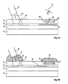
- the Figures 2A and 2B illustrate two steps of a method of aligning an optical fiber on a submicron waveguide.
- a device comprising a support 51, for example of silicon, on which is formed a layer 53 which constitutes a lower layer of an optical cladding.
- a layer 53 which constitutes a lower layer of an optical cladding.
- the core of a submicron waveguide 55 surrounded and covered with a layer 57 forming an upper layer of the optical cladding.
- the various embodiments are described in relation to a structure comprising a coupling device between the optical fiber and the submicron waveguide constituted by a diffraction grating. It will be noted that the method described here can also be applied to structures in which the coupling device is different from a diffraction grating, for example an anamorphic or anamorphic inverse device. In addition, it should be noted that in the description, although the alignment is made between the optical fiber and the coupling device, there is generally speaking of alignment between the optical fiber and the submicron waveguide.
- a diffraction grating 59 On the surface of the core of the submicronic waveguide 55 is formed a diffraction grating 59 which allows the coupling between an optical fiber 61 and the submicron waveguide.
- the optical fiber 61 delivers a light beam 63 in the direction of the diffraction grating 59. Initially, the optical fiber 61 is positioned roughly so that the light beam 63 reaches the diffraction grating. The precise alignment of the optical fiber 61 and the diffraction grating 59 takes place in a subsequent step.
- the end of the optical fiber is placed in a direction forming an angle of between 0 ° and 15 ° to the normal to the surface of the top layer 57.
- the diffraction grating 59 may consist of a set of parallel openings between them formed on the surface of the core of the submicronic waveguide 55.
- the core of the submicron waveguide 55 widens at the level of the grating. diffraction pattern 59 to allow a good coupling between the optical fiber and the submicron waveguide.
- the diffraction grating 59 may consist of a set of parallel metal strips formed between them and forming the surface of the broad part of the core of the submicron waveguide 55.
- trenches 65 are formed at the surface of the upper layer 57, preferably above the widened portion of the core of the submicronic waveguide 55 or the connecting portion between this enlarged portion and the waveguide. trenches 65 extend in the upper layer 57 to the vicinity of the core of the submicronic waveguide 55.
- the stop of the trenches in the upper layer 57 has the advantage of not degrading the operation of the core of the guide of submicron wave 55 after alignment. However, it will also be possible to extend the trenches 65 to contact the core of the submicron waveguide 55.
- the optical fiber 61 is roughly aligned with the diffraction grating 59 and part of the light beam 63 is transmitted into the core of the submicronic waveguide 55 via the diffraction grating 59.
- transmission is represented in Figure 2A by an arrow 67.
- the presence of the trenches 65 allows extraction of a portion of the light from the light beam 67 (arrow 69) towards the outside of the structure.
- the amount of light 67 conveyed in the core of the optical waveguide 55 is maximum.
- the proper alignment of the optical fiber 61 and the submicronic waveguide depends directly on the amount of light 69 extracted from the core of the waveguide 55 by the trenches 65.
- a photodetector device 71 for example a photodiode, is placed in trenches 65. The photodetector device 71 makes it possible to determine the position of the optical fiber 61 allowing a maximum light extraction 69 and therefore the best coupling with the submicron waveguide.
- the Figure 2B illustrates the result of a step performed once the proper alignment of the optical fiber 61 and diffraction grating 59 obtained.
- An adhesive 73 is deposited at the end of the optical fiber 61 to allow it to be held in position.
- the glue 73 is made of a material whose optical index is close to the optical index of the upper layer 57, for example between 0.95 and 1.05 times this index. Thus, the glue has no influence on the light beams flowing between the optical fiber and the submicron waveguide.
- Another glue point 75 is deposited in the trenches 65.
- the glue 75 is deposited during the same step as the glue 73.
- the glue 75 penetrates, from the upper surface of the upper layer 57, into the trenches 65 to fill them.
- the end of the optical fiber 61 closest to the upper layer 57 is placed about 5 microns from the surface of the upper layer 57.
- the glue 73 is deposited on a thickness of between 10 microns and 20 microns for maintaining in position the end of the correct optical fiber 61.
- the lower layer 53 may have a thickness of the order of 2 ⁇ m
- the core of the submicron waveguide 55 may have a thickness of the order of 0.4 ⁇ m.
- the trenches 65 may have a period of the order of 0.5 microns with a filling rate of 50%. These dimensions of the trenches 65 allow a light extraction 69 of the order of 0.5% of the light guided by the core of the submicron waveguide 55 for a light beam having a wavelength of 1.55 microns.
- the core of the submicron waveguide 55 may be silicon (optical index equal to 3.44) and the lower layers 53 and greater 57 in silicon oxide (optical index equal to 1.44).
- SOI type substrate silicon insulator substrate
- the glue 73 and 75 can be any adhesive material having an optical index between 1.40 and 1.48, for example epoxy, silicone or acrylate.
- the figure 3 illustrates a final step obtained from a variant in which the main elements of the device are identical to those of the Figure 2B .
- the trenches 65 are replaced by a single opening 77 formed in the upper layer 57, above the core of the submicronic waveguide 55.
- the walls of the opening 77 are inclined, the opening widening towards outside.
- the alignment of the optical fiber 61 has been achieved and the glue 75 has been deposited in the aperture 77 to fill it completely. This prevents the passage of a light beam from the core of the submicronic waveguide 55 into the aperture 77.
- a single opening with inclined walls such as the aperture 77 enables less light than a set of parallel openings such as trenches 65 Figures 2A and 2B but this will be enough in many cases.
- the figure 4 is a top view of a structure substantially identical to that of the Figure 2A .
- a light beam 63 from an optical fiber illuminates a diffraction grating 59 formed on the surface of an enlarged portion of the core of a submicronic waveguide 55.
- the diffraction grating 59 and the heart of the guide Sub-micron waves 55 are covered with an upper layer 57.
- Trenches 65 are formed on the surface of the upper layer 57.
- a cavity 79 is formed, in the upper layer 57, on one side of the trenches 65 and contact them.
- the cavity 79 makes it possible to assist in filling the trenches 65 with the glue 75. Indeed, in order to deposit the glue 75, it is deposited in the cavity 79 and, by capillarity, the glue enters the trenches 65 and fills them.
- the coupling device represented in Figures 2A, 2B , 3 and 4 between the optical fiber and the submicron waveguide is a diffraction grating
- the method described here can also be used in connection with other coupling devices, for example anamorphic device or reverse anamorphic device.
- anamorphic device one or more openings in the upper portion of the optical cladding surrounding the core of the submicron waveguide will be provided in the same manner as described above.
- the optical fiber is aligned on one of the sides of the support comprising the submicron waveguide, and therefore that the glue 73 is deposited on the edge of this support.
- structures similar to those presented herein may be formed using different core and sheath materials from those exemplified in this specification.
Landscapes
- Physics & Mathematics (AREA)
- General Physics & Mathematics (AREA)
- Optics & Photonics (AREA)
- Optical Couplings Of Light Guides (AREA)
- Optical Integrated Circuits (AREA)
Claims (9)
- Ein Verfahren zum Ausrichten einer optischen Faser (61) und ein Submikron-Wellenleiter eines integrierten optischen Schaltkreises, wobei der Wellenleiter einen Kern (55) aufweist, der umgeben ist von oberen (57) und unteren (53) Schichten, die eine optische Hülle bilden, wobei das Verfahren die folgenden Schritte aufweist:(a) Ausbilden, in der oberen Schicht (57), von einer oder mehreren Öffnungen (65; 77), die geeignet sind Licht von dem Wellenleiter zu extrahieren;(b) grobes Positionieren der optischen Faser (61), um Licht in den Wellenleiter zu senden;(c) genaues Bewegen der optischen Faser (61) bezüglich des Wellenleiters und Detektieren der Position, die das Extrahieren des maximalen Betrags von Licht auf der Höhe der Öffnung(en) (65; 77) verursacht; und(d) Aufbringen eines Klebers (73, 75) mit einem Brechungsindex nahe dem Brechungsindex der oberen Schicht (57), der die optische Faser mit dem optischen Schaltkreis verbindet und die Öffnung(en) (65; 77) füllt.
- Das Verfahren nach Anspruch 1, wobei der Brechungsindex des Klebers (73, 75) im Bereich von 0,95 bis 1,05 mal den Brechungsindex der oberen Schicht (57) liegt.
- Das Verfahren nach Anspruch 1 oder 2, wobei der Schritt (b) das Positionieren der optischen Faser aufweist, so, dass sie eine optische Verbindungsvorrichtung (59) beleuchtet, die mit dem Wellenleiter assoziiert ist.
- Das Verfahren nach einem der Ansprüche 1 bis 3, wobei die Öffnungen (65) ein Beugungsgitter bilden.
- Das Verfahren nach Anspruch 4, wobei das Verfahren ferner einen Schritt des Ausbildens eines Hohlraums (79) in der oberen Schicht (57) aufweist, die in Kontakt mit den Öffnungen (65) ist, wobei der Kleber (75) in den Hohlraum eingebracht wird und durch Kapillarwirkung in das Beugungsgitter eindringt.
- Das Verfahren nach einem der Ansprüche 1 bis 3, wobei eine einzelne Öffnung (77) mit geneigten Wänden in der oberen Schicht (57) ausgebildet ist.
- Das Verfahren nach einem der Ansprüche 1 bis 6, wobei die obere Schicht (57) aus Siliziumoxid besteht, der Kern (55) aus Silizium besteht und der Kleber (73, 75) einen Brechungsindex im Bereich von 1,40 und 1,48 aufweist.
- Eine optische Vorrichtung, wobei die Vorrichtung Folgendes aufweist:eine optische Faser (61), die mit einem Submikron- Wellenleiter eines integrierten optischen Schaltkreises ausgerichtet ist, wobei der Wellenleiter einen Kern (55) aufweist, der umgeben ist von oberen (57) und unteren (53) Schichten, die eine optische Hülle bilden, wobei die optische Faser in ihrer Position durch einen Kleber (73) gehalten wird, der einen Brechungsindex im Bereich von 0,95 bis 1,05 mal den Brechungsindex der oberen Schicht (57) aufweist; undeine oder mehrere Öffnungen (65; 77), die in der oberen Schicht (57) ausgebildet sind, wobei die Öffnung(en) mit dem Kleber (75) gefüllt sind,und wobei die Öffnungen ein Beugungsgitter in der oberen Schicht (57) ausbilden.
- Die Vorrichtung nach Anspruch 8, wobei die obere Schicht (57) aus Siliziumoxid besteht und der Kern (55) aus Silizium besteht.
Applications Claiming Priority (1)
| Application Number | Priority Date | Filing Date | Title |
|---|---|---|---|
| FR0950779A FR2942047B1 (fr) | 2009-02-09 | 2009-02-09 | Structure et procede d'alignement d'une fibre optique et d'un guide d'ondes submicronique |
Publications (2)
| Publication Number | Publication Date |
|---|---|
| EP2216663A1 EP2216663A1 (de) | 2010-08-11 |
| EP2216663B1 true EP2216663B1 (de) | 2011-10-19 |
Family
ID=41022388
Family Applications (1)
| Application Number | Title | Priority Date | Filing Date |
|---|---|---|---|
| EP10152313A Not-in-force EP2216663B1 (de) | 2009-02-09 | 2010-02-01 | Struktur und Verfahren zur Justierung einer optischen Faser mit einem sub-mikronischen Lichtwellenleiter |
Country Status (4)
| Country | Link |
|---|---|
| US (1) | US20100202738A1 (de) |
| EP (1) | EP2216663B1 (de) |
| AT (1) | ATE529771T1 (de) |
| FR (1) | FR2942047B1 (de) |
Families Citing this family (9)
| Publication number | Priority date | Publication date | Assignee | Title |
|---|---|---|---|---|
| KR20120137839A (ko) * | 2011-06-13 | 2012-12-24 | 삼성전자주식회사 | 광 통신부를 갖는 반도체 소자 |
| WO2013058769A1 (en) * | 2011-10-21 | 2013-04-25 | Hewlett-Packard Development Company, L.P. | Grating couplers with deep-groove non-uniform gratings |
| US9235097B2 (en) | 2012-02-03 | 2016-01-12 | Micron Technology, Inc. | Active alignment of optical fiber to chip using liquid crystals |
| KR20150037880A (ko) | 2012-07-30 | 2015-04-08 | 휴렛-팩커드 디벨롭먼트 컴퍼니, 엘.피. | 광 커플링 시스템 및 그 제조 방법 |
| US9274283B1 (en) * | 2014-09-30 | 2016-03-01 | Globalfoundries Inc. | Silicon photonics alignment tolerant vertical grating couplers |
| JP6770361B2 (ja) * | 2016-07-28 | 2020-10-14 | 富士通株式会社 | 光配線モジュール、光トランシーバ、及び光接続方法 |
| JP7478952B2 (ja) * | 2020-06-04 | 2024-05-08 | パナソニックIpマネジメント株式会社 | 光モジュール及び光導波路接続方法 |
| CN113671638A (zh) * | 2021-07-12 | 2021-11-19 | 武汉英飞光创科技有限公司 | 一种光模块 |
| CN119063871B (zh) * | 2024-10-11 | 2025-09-26 | 中电普瑞电力工程有限公司 | 一种可实现igbt内部准分布式温度检测的光子传感器 |
Family Cites Families (24)
| Publication number | Priority date | Publication date | Assignee | Title |
|---|---|---|---|---|
| US4221465A (en) * | 1978-09-28 | 1980-09-09 | Rca Corporation | Patching tape for diffractive subtractive filter viewgraphs |
| DE3687162D1 (de) * | 1985-12-10 | 1993-01-07 | Siemens Ag | Integriert-optischer multiplex-demultiplex-modul fuer die optische nachrichtenuebertragung. |
| DE3786497T2 (de) * | 1986-07-18 | 1994-02-17 | Nippon Electric Co | Doppelbrechendes Beugungsgitter und optischer Kopf, in welchem ein linearpolarisierter Strahl auf dieses Gitter gelenkt wird. |
| US4745293A (en) * | 1987-03-23 | 1988-05-17 | Cv Technology, Inc. | Method and apparatus for optically measuring fluid levels |
| CN1134677C (zh) * | 1994-04-14 | 2004-01-14 | 株式会社三协精机制作所 | 偏振光束分束器及使用偏振光束分束器的光探头 |
| US20020110328A1 (en) * | 2001-02-14 | 2002-08-15 | Bischel William K. | Multi-channel laser pump source for optical amplifiers |
| JP2002311242A (ja) * | 2001-04-18 | 2002-10-23 | Ricoh Co Ltd | 偏光分離素子、半導体レーザユニットおよび光ピックアップ装置 |
| US6904200B2 (en) * | 2001-09-14 | 2005-06-07 | Fibera, Inc. | Multidimensional optical gratings |
| EP1474710B1 (de) * | 2002-02-12 | 2008-12-31 | OC Oerlikon Balzers AG | Optisches bauteil mit submikrometer-hohlräumen |
| GB2385678A (en) * | 2002-02-20 | 2003-08-27 | Bookham Technology Plc | Mthod of joining optical components using adhesive |
| US20040114642A1 (en) * | 2002-03-22 | 2004-06-17 | Bullington Jeff A. | Laser diode with output fiber feedback |
| US7184625B2 (en) * | 2003-02-11 | 2007-02-27 | Luxtera, Inc | Optical waveguide grating coupler incorporating reflective optical elements and anti-reflection elements |
| US7162124B1 (en) * | 2003-03-14 | 2007-01-09 | Luxtera, Inc. | Fiber to chip coupler |
| US20050135727A1 (en) * | 2003-12-18 | 2005-06-23 | Sioptical, Inc. | EMI-EMC shield for silicon-based optical transceiver |
| JP4308050B2 (ja) * | 2004-03-18 | 2009-08-05 | 三洋電機株式会社 | 光導波路 |
| US20050207706A1 (en) * | 2004-03-19 | 2005-09-22 | Schmidt Terrance J | Method of radiusing and beam profiling optical fiber tips mounted in a polishing fixture and apparatus used therefor |
| US7027677B2 (en) * | 2004-05-19 | 2006-04-11 | Intel Corporation | Integrating optical components on a planar light circuit |
| US7283695B2 (en) * | 2004-08-31 | 2007-10-16 | Georgia Tech Research Corporation | Optical interconnects in microelectronics based on azimuthally asymmetric long-period fiber grating couplers |
| US7433563B2 (en) * | 2005-05-25 | 2008-10-07 | University Of Vermont And State Agricultural College | Optical fiber microscopy launch system and method |
| JP4452743B2 (ja) * | 2005-06-10 | 2010-04-21 | 富士通株式会社 | 光モジュールの製造方法、光モジュール及び光モジュール用プラットフォーム |
| JP2007094350A (ja) * | 2005-09-28 | 2007-04-12 | Korea Electronics Telecommun | 光ファイバを利用した波長選別式光集束装置及びそれを利用した光モジュール |
| US20080069497A1 (en) * | 2006-09-15 | 2008-03-20 | Yann Tissot | Optical waveguide tap monitor |
| KR101450934B1 (ko) * | 2007-04-06 | 2014-10-14 | 아사히 가라스 가부시키가이샤 | 광헤드 장치 |
| EP2009416A1 (de) * | 2007-06-29 | 2008-12-31 | Interuniversitair Microelektronica Centrum Vzw | Optische Sonde |
-
2009
- 2009-02-09 FR FR0950779A patent/FR2942047B1/fr not_active Expired - Fee Related
-
2010
- 2010-02-01 EP EP10152313A patent/EP2216663B1/de not_active Not-in-force
- 2010-02-01 AT AT10152313T patent/ATE529771T1/de not_active IP Right Cessation
- 2010-02-08 US US12/701,750 patent/US20100202738A1/en not_active Abandoned
Also Published As
| Publication number | Publication date |
|---|---|
| US20100202738A1 (en) | 2010-08-12 |
| EP2216663A1 (de) | 2010-08-11 |
| FR2942047B1 (fr) | 2011-06-17 |
| ATE529771T1 (de) | 2011-11-15 |
| FR2942047A1 (fr) | 2010-08-13 |
Similar Documents
| Publication | Publication Date | Title |
|---|---|---|
| EP2216663B1 (de) | Struktur und Verfahren zur Justierung einer optischen Faser mit einem sub-mikronischen Lichtwellenleiter | |
| EP3715925B1 (de) | Chip für photonischen integrierten schaltkreis | |
| EP2286289B1 (de) | Vorrichtung zum kuppeln einer glasfaser und einer nanophotonischen komponente | |
| FR3066615B1 (fr) | Puce photonique a structure de collimation integree | |
| EP2267500A2 (de) | Ausrichtungsstruktur und -verfahren einer optischen Faser und eines submikroskopischen Wellenleiters | |
| EP2177938A1 (de) | Ausrichtungsstruktur und -verfahren einer optischen Faser auf einem optischen Wellenleiter | |
| EP1269238B1 (de) | Verfahren und vorrichtung für optische fasern und optoelektronische bauelemente passiver ausrichtung | |
| CA2084355A1 (fr) | Composant optique semi-conducteur a mode de sortie elargi et son procede de fabrication | |
| FR3066617A1 (fr) | Puce photonique a structure reflechissante de repliement de trajet optique | |
| FR3027689A1 (fr) | Structure de couplage lumineux et dispositif optique comprenant un coupleur a reseau | |
| FR3028324A1 (de) | ||
| EP3538937B1 (de) | Verfahren zur gemeinsamen herstellung einer vielzahl von optoelektronischen chips | |
| EP2410361B1 (de) | Planarer, nanophotonischer Wellenleiter, der eine optische Kupplungsstruktur mit einer optischen Faser umfasst | |
| FR2906896A1 (fr) | Dispositif de couplage ameliore entre une fibre optique et un guide optique integre sur un substrat. | |
| EP0950906A1 (de) | Verfahren zum Zusammenbauen eines optischen Moduls | |
| EP1160602A1 (de) | Ausrichtung eines Flipchiplasers in einer schrägen Position auf einer Montageebene mit Ausrichtpfosten | |
| FR3071327B1 (fr) | Procede et systeme d'alignement de l'axe optique d'un cable optique avec un composant optoelectronique | |
| EP1202085B1 (de) | Verfahren zum Herstellen eines optischen Wellenleiters und Kopplungsvorrichtung mit einem solchen Leiter | |
| FR3143780A1 (fr) | Dispositif de couplage optique à structure de diffraction holographique | |
| FR2830628A1 (fr) | Support de positionnement et de maintien de fibres optiques et procede de realisation d'un tel support | |
| FR2851826A1 (fr) | Coupleur optique pour circuits integres a guide d'onde optique | |
| FR2941058A1 (fr) | Dispositif de transmission optique a fibre optique couplee par ondes evanescentes a un guide d'onde planaire | |
| WO2018122493A1 (fr) | Dispositif de collimation | |
| FR2815139A1 (fr) | Procede et dispositif d'alignement passif d'un connecteur optique multifibres et d'un composant optique | |
| FR2950440A1 (fr) | Dispositif de couplage entre une fibre optique et un guide d'ondes nanophotonique |
Legal Events
| Date | Code | Title | Description |
|---|---|---|---|
| PUAI | Public reference made under article 153(3) epc to a published international application that has entered the european phase |
Free format text: ORIGINAL CODE: 0009012 |
|
| AK | Designated contracting states |
Kind code of ref document: A1 Designated state(s): AT BE BG CH CY CZ DE DK EE ES FI FR GB GR HR HU IE IS IT LI LT LU LV MC MK MT NL NO PL PT RO SE SI SK SM TR |
|
| AX | Request for extension of the european patent |
Extension state: AL BA RS |
|
| 17P | Request for examination filed |
Effective date: 20110204 |
|
| RIC1 | Information provided on ipc code assigned before grant |
Ipc: G02B 6/42 20060101ALI20110307BHEP Ipc: G02B 6/30 20060101AFI20110307BHEP |
|
| GRAP | Despatch of communication of intention to grant a patent |
Free format text: ORIGINAL CODE: EPIDOSNIGR1 |
|
| GRAS | Grant fee paid |
Free format text: ORIGINAL CODE: EPIDOSNIGR3 |
|
| GRAA | (expected) grant |
Free format text: ORIGINAL CODE: 0009210 |
|
| AK | Designated contracting states |
Kind code of ref document: B1 Designated state(s): AT BE BG CH CY CZ DE DK EE ES FI FR GB GR HR HU IE IS IT LI LT LU LV MC MK MT NL NO PL PT RO SE SI SK SM TR |
|
| REG | Reference to a national code |
Ref country code: GB Ref legal event code: FG4D Free format text: NOT ENGLISH |
|
| REG | Reference to a national code |
Ref country code: CH Ref legal event code: EP |
|
| REG | Reference to a national code |
Ref country code: IE Ref legal event code: FG4D |
|
| REG | Reference to a national code |
Ref country code: DE Ref legal event code: R096 Ref document number: 602010000271 Country of ref document: DE Effective date: 20120112 |
|
| REG | Reference to a national code |
Ref country code: NL Ref legal event code: VDEP Effective date: 20111019 |
|
| LTIE | Lt: invalidation of european patent or patent extension |
Effective date: 20111019 |
|
| REG | Reference to a national code |
Ref country code: AT Ref legal event code: MK05 Ref document number: 529771 Country of ref document: AT Kind code of ref document: T Effective date: 20111019 |
|
| PG25 | Lapsed in a contracting state [announced via postgrant information from national office to epo] |
Ref country code: IS Free format text: LAPSE BECAUSE OF FAILURE TO SUBMIT A TRANSLATION OF THE DESCRIPTION OR TO PAY THE FEE WITHIN THE PRESCRIBED TIME-LIMIT Effective date: 20120219 Ref country code: LT Free format text: LAPSE BECAUSE OF FAILURE TO SUBMIT A TRANSLATION OF THE DESCRIPTION OR TO PAY THE FEE WITHIN THE PRESCRIBED TIME-LIMIT Effective date: 20111019 Ref country code: NO Free format text: LAPSE BECAUSE OF FAILURE TO SUBMIT A TRANSLATION OF THE DESCRIPTION OR TO PAY THE FEE WITHIN THE PRESCRIBED TIME-LIMIT Effective date: 20120119 |
|
| REG | Reference to a national code |
Ref country code: IE Ref legal event code: FD4D |
|
| PG25 | Lapsed in a contracting state [announced via postgrant information from national office to epo] |
Ref country code: SI Free format text: LAPSE BECAUSE OF FAILURE TO SUBMIT A TRANSLATION OF THE DESCRIPTION OR TO PAY THE FEE WITHIN THE PRESCRIBED TIME-LIMIT Effective date: 20111019 Ref country code: PT Free format text: LAPSE BECAUSE OF FAILURE TO SUBMIT A TRANSLATION OF THE DESCRIPTION OR TO PAY THE FEE WITHIN THE PRESCRIBED TIME-LIMIT Effective date: 20120220 Ref country code: NL Free format text: LAPSE BECAUSE OF FAILURE TO SUBMIT A TRANSLATION OF THE DESCRIPTION OR TO PAY THE FEE WITHIN THE PRESCRIBED TIME-LIMIT Effective date: 20111019 Ref country code: HR Free format text: LAPSE BECAUSE OF FAILURE TO SUBMIT A TRANSLATION OF THE DESCRIPTION OR TO PAY THE FEE WITHIN THE PRESCRIBED TIME-LIMIT Effective date: 20111019 Ref country code: SE Free format text: LAPSE BECAUSE OF FAILURE TO SUBMIT A TRANSLATION OF THE DESCRIPTION OR TO PAY THE FEE WITHIN THE PRESCRIBED TIME-LIMIT Effective date: 20111019 Ref country code: LV Free format text: LAPSE BECAUSE OF FAILURE TO SUBMIT A TRANSLATION OF THE DESCRIPTION OR TO PAY THE FEE WITHIN THE PRESCRIBED TIME-LIMIT Effective date: 20111019 Ref country code: GR Free format text: LAPSE BECAUSE OF FAILURE TO SUBMIT A TRANSLATION OF THE DESCRIPTION OR TO PAY THE FEE WITHIN THE PRESCRIBED TIME-LIMIT Effective date: 20120120 |
|
| PG25 | Lapsed in a contracting state [announced via postgrant information from national office to epo] |
Ref country code: CY Free format text: LAPSE BECAUSE OF FAILURE TO SUBMIT A TRANSLATION OF THE DESCRIPTION OR TO PAY THE FEE WITHIN THE PRESCRIBED TIME-LIMIT Effective date: 20111019 |
|
| PG25 | Lapsed in a contracting state [announced via postgrant information from national office to epo] |
Ref country code: EE Free format text: LAPSE BECAUSE OF FAILURE TO SUBMIT A TRANSLATION OF THE DESCRIPTION OR TO PAY THE FEE WITHIN THE PRESCRIBED TIME-LIMIT Effective date: 20111019 Ref country code: SK Free format text: LAPSE BECAUSE OF FAILURE TO SUBMIT A TRANSLATION OF THE DESCRIPTION OR TO PAY THE FEE WITHIN THE PRESCRIBED TIME-LIMIT Effective date: 20111019 Ref country code: IE Free format text: LAPSE BECAUSE OF FAILURE TO SUBMIT A TRANSLATION OF THE DESCRIPTION OR TO PAY THE FEE WITHIN THE PRESCRIBED TIME-LIMIT Effective date: 20111019 Ref country code: BG Free format text: LAPSE BECAUSE OF FAILURE TO SUBMIT A TRANSLATION OF THE DESCRIPTION OR TO PAY THE FEE WITHIN THE PRESCRIBED TIME-LIMIT Effective date: 20120119 Ref country code: DK Free format text: LAPSE BECAUSE OF FAILURE TO SUBMIT A TRANSLATION OF THE DESCRIPTION OR TO PAY THE FEE WITHIN THE PRESCRIBED TIME-LIMIT Effective date: 20111019 Ref country code: CZ Free format text: LAPSE BECAUSE OF FAILURE TO SUBMIT A TRANSLATION OF THE DESCRIPTION OR TO PAY THE FEE WITHIN THE PRESCRIBED TIME-LIMIT Effective date: 20111019 |
|
| PLBE | No opposition filed within time limit |
Free format text: ORIGINAL CODE: 0009261 |
|
| STAA | Information on the status of an ep patent application or granted ep patent |
Free format text: STATUS: NO OPPOSITION FILED WITHIN TIME LIMIT |
|
| BERE | Be: lapsed |
Owner name: COMMISSARIAT A L'ENERGIE ATOMIQUE ET AUX ENERGIES Effective date: 20120228 |
|
| PG25 | Lapsed in a contracting state [announced via postgrant information from national office to epo] |
Ref country code: PL Free format text: LAPSE BECAUSE OF FAILURE TO SUBMIT A TRANSLATION OF THE DESCRIPTION OR TO PAY THE FEE WITHIN THE PRESCRIBED TIME-LIMIT Effective date: 20111019 Ref country code: RO Free format text: LAPSE BECAUSE OF FAILURE TO SUBMIT A TRANSLATION OF THE DESCRIPTION OR TO PAY THE FEE WITHIN THE PRESCRIBED TIME-LIMIT Effective date: 20111019 |
|
| 26N | No opposition filed |
Effective date: 20120720 |
|
| PG25 | Lapsed in a contracting state [announced via postgrant information from national office to epo] |
Ref country code: MC Free format text: LAPSE BECAUSE OF NON-PAYMENT OF DUE FEES Effective date: 20120229 |
|
| REG | Reference to a national code |
Ref country code: DE Ref legal event code: R097 Ref document number: 602010000271 Country of ref document: DE Effective date: 20120720 |
|
| PG25 | Lapsed in a contracting state [announced via postgrant information from national office to epo] |
Ref country code: BE Free format text: LAPSE BECAUSE OF NON-PAYMENT OF DUE FEES Effective date: 20120228 |
|
| PG25 | Lapsed in a contracting state [announced via postgrant information from national office to epo] |
Ref country code: AT Free format text: LAPSE BECAUSE OF FAILURE TO SUBMIT A TRANSLATION OF THE DESCRIPTION OR TO PAY THE FEE WITHIN THE PRESCRIBED TIME-LIMIT Effective date: 20111019 |
|
| PG25 | Lapsed in a contracting state [announced via postgrant information from national office to epo] |
Ref country code: MK Free format text: LAPSE BECAUSE OF FAILURE TO SUBMIT A TRANSLATION OF THE DESCRIPTION OR TO PAY THE FEE WITHIN THE PRESCRIBED TIME-LIMIT Effective date: 20111019 |
|
| PG25 | Lapsed in a contracting state [announced via postgrant information from national office to epo] |
Ref country code: ES Free format text: LAPSE BECAUSE OF FAILURE TO SUBMIT A TRANSLATION OF THE DESCRIPTION OR TO PAY THE FEE WITHIN THE PRESCRIBED TIME-LIMIT Effective date: 20120130 |
|
| PG25 | Lapsed in a contracting state [announced via postgrant information from national office to epo] |
Ref country code: FI Free format text: LAPSE BECAUSE OF FAILURE TO SUBMIT A TRANSLATION OF THE DESCRIPTION OR TO PAY THE FEE WITHIN THE PRESCRIBED TIME-LIMIT Effective date: 20111019 |
|
| PG25 | Lapsed in a contracting state [announced via postgrant information from national office to epo] |
Ref country code: MT Free format text: LAPSE BECAUSE OF FAILURE TO SUBMIT A TRANSLATION OF THE DESCRIPTION OR TO PAY THE FEE WITHIN THE PRESCRIBED TIME-LIMIT Effective date: 20111019 |
|
| PG25 | Lapsed in a contracting state [announced via postgrant information from national office to epo] |
Ref country code: TR Free format text: LAPSE BECAUSE OF FAILURE TO SUBMIT A TRANSLATION OF THE DESCRIPTION OR TO PAY THE FEE WITHIN THE PRESCRIBED TIME-LIMIT Effective date: 20111019 |
|
| PG25 | Lapsed in a contracting state [announced via postgrant information from national office to epo] |
Ref country code: SM Free format text: LAPSE BECAUSE OF FAILURE TO SUBMIT A TRANSLATION OF THE DESCRIPTION OR TO PAY THE FEE WITHIN THE PRESCRIBED TIME-LIMIT Effective date: 20111019 Ref country code: LU Free format text: LAPSE BECAUSE OF NON-PAYMENT OF DUE FEES Effective date: 20120201 |
|
| PG25 | Lapsed in a contracting state [announced via postgrant information from national office to epo] |
Ref country code: HU Free format text: LAPSE BECAUSE OF FAILURE TO SUBMIT A TRANSLATION OF THE DESCRIPTION OR TO PAY THE FEE WITHIN THE PRESCRIBED TIME-LIMIT Effective date: 20100201 |
|
| REG | Reference to a national code |
Ref country code: CH Ref legal event code: PL |
|
| PG25 | Lapsed in a contracting state [announced via postgrant information from national office to epo] |
Ref country code: LI Free format text: LAPSE BECAUSE OF NON-PAYMENT OF DUE FEES Effective date: 20140228 Ref country code: CH Free format text: LAPSE BECAUSE OF NON-PAYMENT OF DUE FEES Effective date: 20140228 |
|
| REG | Reference to a national code |
Ref country code: FR Ref legal event code: PLFP Year of fee payment: 6 |
|
| PGFP | Annual fee paid to national office [announced via postgrant information from national office to epo] |
Ref country code: IT Payment date: 20150226 Year of fee payment: 6 Ref country code: DE Payment date: 20150210 Year of fee payment: 6 |
|
| PGFP | Annual fee paid to national office [announced via postgrant information from national office to epo] |
Ref country code: GB Payment date: 20150216 Year of fee payment: 6 Ref country code: FR Payment date: 20150218 Year of fee payment: 6 |
|
| REG | Reference to a national code |
Ref country code: DE Ref legal event code: R119 Ref document number: 602010000271 Country of ref document: DE |
|
| GBPC | Gb: european patent ceased through non-payment of renewal fee |
Effective date: 20160201 |
|
| REG | Reference to a national code |
Ref country code: FR Ref legal event code: ST Effective date: 20161028 |
|
| PG25 | Lapsed in a contracting state [announced via postgrant information from national office to epo] |
Ref country code: IT Free format text: LAPSE BECAUSE OF NON-PAYMENT OF DUE FEES Effective date: 20160201 |
|
| PG25 | Lapsed in a contracting state [announced via postgrant information from national office to epo] |
Ref country code: FR Free format text: LAPSE BECAUSE OF NON-PAYMENT OF DUE FEES Effective date: 20160229 Ref country code: GB Free format text: LAPSE BECAUSE OF NON-PAYMENT OF DUE FEES Effective date: 20160201 Ref country code: DE Free format text: LAPSE BECAUSE OF NON-PAYMENT OF DUE FEES Effective date: 20160901 |