EP2216801A2 - Dispositif électrique doté d'une alimentation électrique ayant un condensateur magnétique en tant que dispositif de stockage d'énergie - Google Patents
Dispositif électrique doté d'une alimentation électrique ayant un condensateur magnétique en tant que dispositif de stockage d'énergie Download PDFInfo
- Publication number
- EP2216801A2 EP2216801A2 EP10152697A EP10152697A EP2216801A2 EP 2216801 A2 EP2216801 A2 EP 2216801A2 EP 10152697 A EP10152697 A EP 10152697A EP 10152697 A EP10152697 A EP 10152697A EP 2216801 A2 EP2216801 A2 EP 2216801A2
- Authority
- EP
- European Patent Office
- Prior art keywords
- electrical device
- integrated circuit
- magnetic
- circuit chip
- section
- Prior art date
- Legal status (The legal status is an assumption and is not a legal conclusion. Google has not performed a legal analysis and makes no representation as to the accuracy of the status listed.)
- Withdrawn
Links
Images




Classifications
-
- H—ELECTRICITY
- H10—SEMICONDUCTOR DEVICES; ELECTRIC SOLID-STATE DEVICES NOT OTHERWISE PROVIDED FOR
- H10D—INORGANIC ELECTRIC SEMICONDUCTOR DEVICES
- H10D1/00—Resistors, capacitors or inductors
- H10D1/60—Capacitors
- H10D1/68—Capacitors having no potential barriers
- H10D1/692—Electrodes
-
- H—ELECTRICITY
- H01—ELECTRIC ELEMENTS
- H01G—CAPACITORS; CAPACITORS, RECTIFIERS, DETECTORS, SWITCHING DEVICES, LIGHT-SENSITIVE OR TEMPERATURE-SENSITIVE DEVICES OF THE ELECTROLYTIC TYPE
- H01G4/00—Fixed capacitors; Processes of their manufacture
- H01G4/002—Details
- H01G4/005—Electrodes
- H01G4/008—Selection of materials
-
- H—ELECTRICITY
- H02—GENERATION; CONVERSION OR DISTRIBUTION OF ELECTRIC POWER
- H02S—GENERATION OF ELECTRIC POWER BY CONVERSION OF INFRARED RADIATION, VISIBLE LIGHT OR ULTRAVIOLET LIGHT, e.g. USING PHOTOVOLTAIC [PV] MODULES
- H02S40/00—Components or accessories in combination with PV modules, not provided for in groups H02S10/00 - H02S30/00
- H02S40/30—Electrical components
- H02S40/38—Energy storage means, e.g. batteries, structurally associated with PV modules
-
- H—ELECTRICITY
- H10—SEMICONDUCTOR DEVICES; ELECTRIC SOLID-STATE DEVICES NOT OTHERWISE PROVIDED FOR
- H10D—INORGANIC ELECTRIC SEMICONDUCTOR DEVICES
- H10D1/00—Resistors, capacitors or inductors
- H10D1/60—Capacitors
- H10D1/68—Capacitors having no potential barriers
-
- H—ELECTRICITY
- H10—SEMICONDUCTOR DEVICES; ELECTRIC SOLID-STATE DEVICES NOT OTHERWISE PROVIDED FOR
- H10W—GENERIC PACKAGES, INTERCONNECTIONS, CONNECTORS OR OTHER CONSTRUCTIONAL DETAILS OF DEVICES COVERED BY CLASS H10
- H10W42/00—Arrangements for protection of devices
-
- H—ELECTRICITY
- H10—SEMICONDUCTOR DEVICES; ELECTRIC SOLID-STATE DEVICES NOT OTHERWISE PROVIDED FOR
- H10W—GENERIC PACKAGES, INTERCONNECTIONS, CONNECTORS OR OTHER CONSTRUCTIONAL DETAILS OF DEVICES COVERED BY CLASS H10
- H10W44/00—Electrical arrangements for controlling or matching impedance
- H10W44/20—Electrical arrangements for controlling or matching impedance at high-frequency [HF] or radio frequency [RF]
-
- H—ELECTRICITY
- H10—SEMICONDUCTOR DEVICES; ELECTRIC SOLID-STATE DEVICES NOT OTHERWISE PROVIDED FOR
- H10W—GENERIC PACKAGES, INTERCONNECTIONS, CONNECTORS OR OTHER CONSTRUCTIONAL DETAILS OF DEVICES COVERED BY CLASS H10
- H10W44/00—Electrical arrangements for controlling or matching impedance
- H10W44/601—Capacitive arrangements
-
- H—ELECTRICITY
- H10—SEMICONDUCTOR DEVICES; ELECTRIC SOLID-STATE DEVICES NOT OTHERWISE PROVIDED FOR
- H10W—GENERIC PACKAGES, INTERCONNECTIONS, CONNECTORS OR OTHER CONSTRUCTIONAL DETAILS OF DEVICES COVERED BY CLASS H10
- H10W44/00—Electrical arrangements for controlling or matching impedance
- H10W44/20—Electrical arrangements for controlling or matching impedance at high-frequency [HF] or radio frequency [RF]
- H10W44/241—Electrical arrangements for controlling or matching impedance at high-frequency [HF] or radio frequency [RF] for passive devices or passive elements
- H10W44/248—Electrical arrangements for controlling or matching impedance at high-frequency [HF] or radio frequency [RF] for passive devices or passive elements for antennas
-
- H—ELECTRICITY
- H10—SEMICONDUCTOR DEVICES; ELECTRIC SOLID-STATE DEVICES NOT OTHERWISE PROVIDED FOR
- H10W—GENERIC PACKAGES, INTERCONNECTIONS, CONNECTORS OR OTHER CONSTRUCTIONAL DETAILS OF DEVICES COVERED BY CLASS H10
- H10W72/00—Interconnections or connectors in packages
- H10W72/071—Connecting or disconnecting
- H10W72/072—Connecting or disconnecting of bump connectors
- H10W72/07251—Connecting or disconnecting of bump connectors characterised by changes in properties of the bump connectors during connecting
-
- H—ELECTRICITY
- H10—SEMICONDUCTOR DEVICES; ELECTRIC SOLID-STATE DEVICES NOT OTHERWISE PROVIDED FOR
- H10W—GENERIC PACKAGES, INTERCONNECTIONS, CONNECTORS OR OTHER CONSTRUCTIONAL DETAILS OF DEVICES COVERED BY CLASS H10
- H10W72/00—Interconnections or connectors in packages
- H10W72/20—Bump connectors, e.g. solder bumps or copper pillars; Dummy bumps; Thermal bumps
-
- H—ELECTRICITY
- H10—SEMICONDUCTOR DEVICES; ELECTRIC SOLID-STATE DEVICES NOT OTHERWISE PROVIDED FOR
- H10W—GENERIC PACKAGES, INTERCONNECTIONS, CONNECTORS OR OTHER CONSTRUCTIONAL DETAILS OF DEVICES COVERED BY CLASS H10
- H10W72/00—Interconnections or connectors in packages
- H10W72/50—Bond wires
- H10W72/59—Bond pads specially adapted therefor
-
- H—ELECTRICITY
- H10—SEMICONDUCTOR DEVICES; ELECTRIC SOLID-STATE DEVICES NOT OTHERWISE PROVIDED FOR
- H10W—GENERIC PACKAGES, INTERCONNECTIONS, CONNECTORS OR OTHER CONSTRUCTIONAL DETAILS OF DEVICES COVERED BY CLASS H10
- H10W90/00—Package configurations
-
- H—ELECTRICITY
- H10—SEMICONDUCTOR DEVICES; ELECTRIC SOLID-STATE DEVICES NOT OTHERWISE PROVIDED FOR
- H10W—GENERIC PACKAGES, INTERCONNECTIONS, CONNECTORS OR OTHER CONSTRUCTIONAL DETAILS OF DEVICES COVERED BY CLASS H10
- H10W90/00—Package configurations
- H10W90/701—Package configurations characterised by the relative positions of pads or connectors relative to package parts
- H10W90/731—Package configurations characterised by the relative positions of pads or connectors relative to package parts of die-attach connectors
- H10W90/732—Package configurations characterised by the relative positions of pads or connectors relative to package parts of die-attach connectors between stacked chips
-
- H—ELECTRICITY
- H10—SEMICONDUCTOR DEVICES; ELECTRIC SOLID-STATE DEVICES NOT OTHERWISE PROVIDED FOR
- H10W—GENERIC PACKAGES, INTERCONNECTIONS, CONNECTORS OR OTHER CONSTRUCTIONAL DETAILS OF DEVICES COVERED BY CLASS H10
- H10W90/00—Package configurations
- H10W90/701—Package configurations characterised by the relative positions of pads or connectors relative to package parts
- H10W90/751—Package configurations characterised by the relative positions of pads or connectors relative to package parts of bond wires
- H10W90/754—Package configurations characterised by the relative positions of pads or connectors relative to package parts of bond wires between a chip and a stacked insulating package substrate, interposer or RDL
-
- Y—GENERAL TAGGING OF NEW TECHNOLOGICAL DEVELOPMENTS; GENERAL TAGGING OF CROSS-SECTIONAL TECHNOLOGIES SPANNING OVER SEVERAL SECTIONS OF THE IPC; TECHNICAL SUBJECTS COVERED BY FORMER USPC CROSS-REFERENCE ART COLLECTIONS [XRACs] AND DIGESTS
- Y02—TECHNOLOGIES OR APPLICATIONS FOR MITIGATION OR ADAPTATION AGAINST CLIMATE CHANGE
- Y02E—REDUCTION OF GREENHOUSE GAS [GHG] EMISSIONS, RELATED TO ENERGY GENERATION, TRANSMISSION OR DISTRIBUTION
- Y02E10/00—Energy generation through renewable energy sources
- Y02E10/50—Photovoltaic [PV] energy
-
- Y—GENERAL TAGGING OF NEW TECHNOLOGICAL DEVELOPMENTS; GENERAL TAGGING OF CROSS-SECTIONAL TECHNOLOGIES SPANNING OVER SEVERAL SECTIONS OF THE IPC; TECHNICAL SUBJECTS COVERED BY FORMER USPC CROSS-REFERENCE ART COLLECTIONS [XRACs] AND DIGESTS
- Y02—TECHNOLOGIES OR APPLICATIONS FOR MITIGATION OR ADAPTATION AGAINST CLIMATE CHANGE
- Y02E—REDUCTION OF GREENHOUSE GAS [GHG] EMISSIONS, RELATED TO ENERGY GENERATION, TRANSMISSION OR DISTRIBUTION
- Y02E70/00—Other energy conversion or management systems reducing GHG emissions
- Y02E70/30—Systems combining energy storage with energy generation of non-fossil origin
Definitions
- the present invention relates to an electrical device. More particularly, the present invention relates to an electrical device having a power source using a magnetic capacitor as an energy storage device.
- Thin-film batteries are a power source for providing power to a system.
- a thin-film battery provides a constant voltage to the electronic device so that the electronic device may be powered by a stable power source.
- the use of thin-film batteries as power sources for electronic devices suffer from a couple of problems.
- existing thin-film batteries are big and place constraints on the flexing characteristics of the card.
- existing thin-film batteries do not have sufficient power to support a broader range of operations.
- Third, thin-film primary batteries have limited operating and shelf life. Fourth, time required for recharging a thin-film rechargeable battery is long.
- the present invention is directed to an electrical device having a power source using a magnetic capacitor as an energy storage device.
- the present invention discloses an electrical device.
- the electrical device comprises an integrated circuit chip with a positive terminal and a negative terminal, wherein the integrated circuit chip has an energy management function; and a magnetic capacitor connecting with the integrated circuit chip, the magnetic capacitor stores electrical power and provides the electrical power to the integrated circuit chip, wherein the magnetic capacitor comprises: a first magnetic section connected with the positive terminal; a second magnetic section connected with the negative terminal; and a dielectric section configured between the first magnetic section and the second magnetic section; wherein the dielectric section is arranged to store the electrical power.
- Fig. 1 shows a schematic diagram of a magnetic capacitor according to the present invention. It is noticed that other types of the magnetic capacitor can be used in the present invention.
- the magnetic capacitor 100 has a first magnetic section 110, a second magnetic section 120, and a dielectric section 130 configured between the first magnetic section 110 and the second magnetic section 120.
- the dielectric section 130 is arranged to store electrical energy, and the first magnetic section 110 and the second magnetic section 120 with dipoles (such as 115 and 125) are arranged to prevent electrical energy leakage.
- the dielectric section 130 is a thin film, and the dielectric section 130 is composed of dielectric material, such as BaTiO 3 or TiO 3 .
- the apparatus further has a first metal device 140 disposed around the first magnetic section 110, wherein the first metal device 140 is arranged to control the dipole 115 of the first magnetic section 110.
- the apparatus also has a second metal device 150 disposed around the second magnetic section 120, wherein the second metal device 150 is arranged to control the dipole 125 of the second magnetic section 120. The designer or user can use the first metal device 140 and the second metal device 150 to apply external fields to control the dipoles of the magnetic sections 110 and 120.
- the dipoles 115 ( ⁇ ) and 125 ( ⁇ ) of the first magnetic section 110 and the second magnetic section 120 are the same, the first magnetic section 110 and the second magnetic section 120 prevent electrical energy leakage, and electrical energy can be stored in the dielectric section 130.
- the dipoles 115 and 125 of the first magnetic section 110 and the second magnetic section 120 are opposite, the electrical energy stored in the dielectric section 130 can be released.
- Fig. 2 shows the apparatus when the apparatus is charging according to an embodiment of the invention.
- the dipoles 115 and 125 of the first magnetic section 110 and the second magnetic section 120 are controlled to be opposite and the first magnetic section 110 and the second magnetic section 120 are coupled to a power source 260.
- the electrical energy can be inputted into the dielectric section 130 from the power source 260.
- the dipoles 115 and 125 of the first magnetic section 110 and the second magnetic section 120 are controlled to be same to store the inputted electrical energy.
- the magnetic capacitor is charged by a solar power source.
- Fig 3 illustrates a side cross-sectional view of the magnetic capacitor that is charged by a solar panel.
- the solar panel 320 receives solar energy from sunlight, and the magnetic capacitor 100 stores the solar energy.
- the solar panel 320 has a first side 121 and a second side 122.
- the first side 121 of the solar panel 320 faces the sun, and the second magnetic section 120 of the magnetic capacitor 100 is attached to the second side 122 of the solar panel 320.
- the first magnetic section 110 of the magnetic capacitor 100 is away from the sunlight.
- a first wire 150 is placed between the second side 122 of the solar panel 320 and the second magnetic section 120 of the magnetic capacitor 100.
- a second wire 170 is attached to the first side 121 of the solar panel 320 and the first magnetic section 110 of the magnetic capacitor 100.
- the end of the first wire 150 can be an anode, while the end of the second wire 170 can be a cathode.
- a method of manufacturing the magnetic capacitor that is charged by a solar panel includes the following steps: forming the solar panel 320 having a first side 121 and a second side 122; forming the magnetic capacitor 100 having a first magnetic section 110, a second magnetic section 120, and a dielectric section 130; joining the solar panel 320 and the magnetic capacitor 100 by abutment; placing a first wire 150 in between the second side 122 of the solar panel 320 and the second magnetic section 120 of the magnetic capacitor 100; and attaching a second wire 170 to the first side 121 of the solar panel 320 and the first magnetic section 110 of the magnetic capacitor 100.
- the end of the first wire 150 forms an anode, while the end of the second wire 170 forms a cathode.
- the solar panel 320 and the magnetic capacitor 100 are both manufactured on semiconductor manufacturing equipment.
- the solar panel 320 is formed with a high temperature, whereas the magnetic capacitor 100 is formed with a lower temperature.
- the solar panel 320 and the magnetic capacitor 100 are manufactured separately, so the yields would be higher. With metal on the second side 122 of the solar panel 320, and metal on the second magnetic section 120 of the magnetic capacitor 100, it is easy to connect both.
- the magnetic capacitor 100 that stores electrical energy can be used to provide power to integrated circuits (ICs), RF transmission, and Ultra Low Power Electronics Systems such as Smart Cards, RFIDs, and Sensors.
- ICs integrated circuits
- RF transmission RF transmission
- Ultra Low Power Electronics Systems such as Smart Cards, RFIDs, and Sensors.
- Fig. 4 shows a magnetic capacitor in a powered smart card.
- the powered smart card 400 includes a card substrate 404, an IC chip 401 and a display 402 both formed on the card substrate 404.
- the IC chip 401 can perform both calculations and memory functions.
- the smart card 400 can generate a one-time password.
- the IC chip 401 can process a program to generate the one-time password.
- the magnetic capacitor 100 is connected to the IC chip 401 to provide power to the IC chip 401 to perform calculations.
- the first magnetic section 110 and the second magnetic section 120 are connected to the positive terminal and the negative terminal of the IC chip 401 respectively.
- the display 402 can show the calculations result, such as the one time password.
- the smart card 400 uses a biometric sensor to detect the user to improve security. The power for the biometric sensor is provided by the magnetic capacitor 100.
- Fig. 5 shows a RFID reader and sensor device.
- the device is a PDA-like battery-driven mobile device.
- the device includes a physical sensor 501 for sensing temperature, pressure, speed, etc., a low-power microcontroller 502, and a low-power, small-range wireless radio frequency connection 503.
- the magnetic capacitor 100 is the power source to provide power to the microcontroller 502.
- the first magnetic section 110 and the second magnetic section 120 are connected to the positive terminal and the negative terminal of the microcontroller 502 respectively.
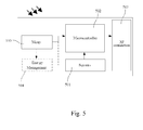
- a solar panel 320 is used to charge the magnetic capacitor 100.
- the structure of the solar panel 320 and the magnetic capacitor 100 is illustrated in the Fig. 3 .
- an energy management unit 504 manages the power supplied to the microcontroller 502.
- Fig. 6 shows a magnetic capacitor providing power to RF transmission.
- the RF transmission 600 includes a tag substrate 601, an antenna 603 formed on the tag substrate 601 and an RFID ASIC 602 surrounded by the antenna 603.
- a magnetic capacitor 100 is connected to the RFID ASIC 602 for supplying power to the RFID ASIC 602.
- the first magnetic section 110 and the second magnetic section 120 are connected to the positive terminal and the negative terminal of the RFID ASIC 602 respectively. Because the RF transmission 600 has a power source, and the magnetic capacitor 100, the RF transmission 600 is an active RFID tags that can transmit in longer distances.
- Fig. 7 and Fig. 8 show a package structure that includes a magnetic capacitor for providing power to integrated circuits (ICs) chip.
- the package structure 700 includes a substrate 701 with a plurality of solder balls 702.
- An integrated circuits (ICs) chip 703 with power management is formed over the substrate 701 and includes a plurality of solder ball 704 to connect with the substrate 701.
- a magnetic capacitor 100 is formed over the integrated circuits (ICs) chip 703.
- a lead wire 705 connects the positive terminal of the magnetic capacitor 100 with the substrate 701.
- a lead wire 706 connects the negative terminal of the magnetic capacitor 100 with the substrate 701.
- a package material is added around the integrated circuits (ICs) chip 703 and the magnetic capacitor 100 to form the package structure 700 to incorporate with a circuit.
- the package structure 700 can contain several chips, such as a specialized processor 801, DRAM or flash memory 802, all mounted on the same substrate as shown in the Fig. 8 .
- a specialized processor 801, DRAM or flash memory 802 all mounted on the same substrate as shown in the Fig. 8 .
Landscapes
- Engineering & Computer Science (AREA)
- Power Engineering (AREA)
- Chemical & Material Sciences (AREA)
- Materials Engineering (AREA)
- Manufacturing & Machinery (AREA)
- Microelectronics & Electronic Packaging (AREA)
- Fixed Capacitors And Capacitor Manufacturing Machines (AREA)
- Charge And Discharge Circuits For Batteries Or The Like (AREA)
- Semiconductor Integrated Circuits (AREA)
- Credit Cards Or The Like (AREA)
Applications Claiming Priority (1)
| Application Number | Priority Date | Filing Date | Title |
|---|---|---|---|
| US12/366,264 US20100194331A1 (en) | 2009-02-05 | 2009-02-05 | electrical device having a power source with a magnetic capacitor as an energy storage device |
Publications (2)
| Publication Number | Publication Date |
|---|---|
| EP2216801A2 true EP2216801A2 (fr) | 2010-08-11 |
| EP2216801A3 EP2216801A3 (fr) | 2012-04-04 |
Family
ID=42109856
Family Applications (1)
| Application Number | Title | Priority Date | Filing Date |
|---|---|---|---|
| EP10152697A Withdrawn EP2216801A3 (fr) | 2009-02-05 | 2010-02-04 | Dispositif électrique doté d'une alimentation électrique ayant un condensateur magnétique en tant que dispositif de stockage d'énergie |
Country Status (6)
| Country | Link |
|---|---|
| US (1) | US20100194331A1 (fr) |
| EP (1) | EP2216801A3 (fr) |
| JP (1) | JP5206704B2 (fr) |
| KR (1) | KR20100090206A (fr) |
| CN (1) | CN101800445B (fr) |
| TW (1) | TW201030627A (fr) |
Families Citing this family (9)
| Publication number | Priority date | Publication date | Assignee | Title |
|---|---|---|---|---|
| US9607764B2 (en) * | 2010-10-20 | 2017-03-28 | Chun-Yen Chang | Method of fabricating high energy density and low leakage electronic devices |
| DE102013102003A1 (de) | 2013-02-28 | 2014-08-28 | Bundesdruckerei Gmbh | Chipkarte mit integrierten aktiven Komponenten |
| US20150013746A1 (en) * | 2013-07-10 | 2015-01-15 | Alexander Mikhailovich Shukh | Photovoltaic System with Embedded Energy Storage Device |
| US9589726B2 (en) | 2013-10-01 | 2017-03-07 | E1023 Corporation | Magnetically enhanced energy storage systems and methods |
| KR102186145B1 (ko) | 2015-09-17 | 2020-12-03 | 삼성전기주식회사 | 적층 세라믹 커패시터 |
| CN105514508A (zh) * | 2015-12-10 | 2016-04-20 | 连清宏 | 一种薄片电池及使用这种电池的电力供应器 |
| CN107332355B (zh) * | 2017-05-26 | 2018-09-07 | 卓磁(上海)实业发展有限公司 | 一种磁能芯片储存电能的方法 |
| TWI665690B (zh) * | 2017-10-24 | 2019-07-11 | 財團法人工業技術研究院 | 磁性電容元件 |
| FR3095287B1 (fr) * | 2019-04-19 | 2022-11-04 | Linxens Holding | Module de capteur biométrique pour carte à puce et procédé de fabrication d’un tel module |
Citations (1)
| Publication number | Priority date | Publication date | Assignee | Title |
|---|---|---|---|---|
| GB2453606A (en) * | 2007-10-11 | 2009-04-15 | Western Lights Semiconductor Corp | Solar power source |
Family Cites Families (19)
| Publication number | Priority date | Publication date | Assignee | Title |
|---|---|---|---|---|
| US4082991A (en) * | 1974-07-11 | 1978-04-04 | James Nickolas Constant | Superconducting energy system |
| JPS62111479A (ja) * | 1985-11-09 | 1987-05-22 | Sanyo Electric Co Ltd | 光起電力装置 |
| JPH022098A (ja) * | 1988-06-14 | 1990-01-08 | Tonen Corp | Icカード用太陽電池 |
| JPH06267783A (ja) * | 1993-03-16 | 1994-09-22 | Tokuyama Soda Co Ltd | コンデンサー |
| JP4484263B2 (ja) * | 1999-03-24 | 2010-06-16 | 三洋電機株式会社 | 太陽電池装置 |
| US7446434B1 (en) * | 2000-04-07 | 2008-11-04 | Motorola, Inc. | Dual mode power management system |
| WO2003050886A2 (fr) * | 2001-12-13 | 2003-06-19 | Siemens Aktiengesellschaft | Systeme d'energie a couche mince |
| US20050268962A1 (en) * | 2000-04-27 | 2005-12-08 | Russell Gaudiana | Flexible Photovoltaic cells, systems and methods |
| JP3820862B2 (ja) * | 2000-09-22 | 2006-09-13 | セイコーエプソン株式会社 | 携帯型情報処理装置および携帯型情報処理装置の制御方法 |
| AU2003902456A0 (en) * | 2003-05-21 | 2003-06-05 | Sustainable Technologies International Pty Ltd | Photovoltaic power source for wireless electronic devices |
| JP2005032763A (ja) * | 2003-07-07 | 2005-02-03 | Seiko Epson Corp | 半導体装置 |
| US6961263B2 (en) * | 2003-09-08 | 2005-11-01 | Hewlett-Packard Development Company, L.P. | Memory device with a thermally assisted write |
| US7557433B2 (en) * | 2004-10-25 | 2009-07-07 | Mccain Joseph H | Microelectronic device with integrated energy source |
| US6906909B2 (en) * | 2003-10-23 | 2005-06-14 | John E. Stauffer | A C capacitor |
| US7118925B2 (en) * | 2004-12-10 | 2006-10-10 | Texas Instruments Incorporated | Fabrication of a ferromagnetic inductor core and capacitor electrode in a single photo mask step |
| US20060197507A1 (en) * | 2005-03-01 | 2006-09-07 | Chao-Hsiang Wang | Solar electric power supply device that can supply an electric power successively |
| JP2007018197A (ja) * | 2005-07-06 | 2007-01-25 | Teruya:Kk | 不正使用検出機能付きrfidタグ |
| EP2000958A2 (fr) * | 2006-03-30 | 2008-12-10 | Oji Paper Company Limited | Module a ci, entree de ci et corps monte sur un ci |
| US20080174936A1 (en) * | 2007-01-19 | 2008-07-24 | Western Lights Semiconductor Corp. | Apparatus and Method to Store Electrical Energy |
-
2009
- 2009-02-05 US US12/366,264 patent/US20100194331A1/en not_active Abandoned
- 2009-12-28 TW TW098145344A patent/TW201030627A/zh unknown
-
2010
- 2010-02-04 KR KR1020100010333A patent/KR20100090206A/ko not_active Ceased
- 2010-02-04 EP EP10152697A patent/EP2216801A3/fr not_active Withdrawn
- 2010-02-04 CN CN201010112743XA patent/CN101800445B/zh not_active Expired - Fee Related
- 2010-02-05 JP JP2010023686A patent/JP5206704B2/ja not_active Expired - Fee Related
Patent Citations (4)
| Publication number | Priority date | Publication date | Assignee | Title |
|---|---|---|---|---|
| GB2453606A (en) * | 2007-10-11 | 2009-04-15 | Western Lights Semiconductor Corp | Solar power source |
| US20090095338A1 (en) * | 2007-10-11 | 2009-04-16 | James Chyl Lai | Solar power source |
| FR2922383A1 (fr) * | 2007-10-11 | 2009-04-17 | Northern Lights Semiconductor | Source d'energie solaire |
| DE102008005510A1 (de) * | 2007-10-11 | 2009-04-23 | Northern Lights Semiconductor Corp., Saint Paul | Solar-Energiequelle |
Also Published As
| Publication number | Publication date |
|---|---|
| JP5206704B2 (ja) | 2013-06-12 |
| JP2010182307A (ja) | 2010-08-19 |
| TW201030627A (en) | 2010-08-16 |
| EP2216801A3 (fr) | 2012-04-04 |
| US20100194331A1 (en) | 2010-08-05 |
| CN101800445B (zh) | 2013-02-13 |
| KR20100090206A (ko) | 2010-08-13 |
| CN101800445A (zh) | 2010-08-11 |
Similar Documents
| Publication | Publication Date | Title |
|---|---|---|
| EP2216801A2 (fr) | Dispositif électrique doté d'une alimentation électrique ayant un condensateur magnétique en tant que dispositif de stockage d'énergie | |
| Wagih et al. | RF-powered wearable energy harvesting and storage module based on E-textile coplanar waveguide rectenna and supercapacitor | |
| US8368515B2 (en) | Dual mode RFID communication device operating as a reader or tag | |
| US10186897B2 (en) | Scalable harvesting system and method | |
| US6700491B2 (en) | Radio frequency identification tag with thin-film battery for antenna | |
| US6127799A (en) | Method and apparatus for wireless powering and recharging | |
| US20160261031A1 (en) | Wearable Power Harvesting System | |
| KR101519510B1 (ko) | 배터리 보호회로 모듈을 포함하는 식별 모듈 카드 및 이를 포함하는 휴대용 무선단말기 | |
| EP2038980A2 (fr) | Systèmes et procédés de rechargement de batteries à film mince | |
| Dini et al. | A fully-autonomous integrated RF energy harvesting system for wearable applications | |
| CN106295452A (zh) | 一种蓝牙读写器检测设备及其配套的检测方法 | |
| CN219611786U (zh) | 无源nfc芯片及无源电子设备 | |
| CN109463021A (zh) | 电池管理集成电路 | |
| Pournoori et al. | RF energy harvesting system with RFID-enabled charge storage monitoring | |
| CN102484292A (zh) | 具有集成dc-dc转换器的电池组 | |
| CN113690513A (zh) | 电池模块及电子设备 | |
| Rosli et al. | Development of RF energy harvesting technique for Li-Fi application | |
| JP2002291176A (ja) | 2次電池実装集積回路 | |
| CN116137525A (zh) | 驱动电路、触控驱动装置和电子设备 | |
| US20020121878A1 (en) | Battery cover with components mounted thereon | |
| WO2014135920A1 (fr) | Appareil conçu pour commuter un régulateur de puissance d'émission d'un dispositif capteur rfid | |
| KR102874042B1 (ko) | 무선 충전 시스템의 동작 모드 전환 방법 | |
| Torigoe et al. | Development of RF Energy Harvesting Circuit by Multistage and Multiple Connections | |
| US11342258B2 (en) | On-die capacitor | |
| Kim et al. | Flexible Energy Harvesting System for Wearable IoT Sensor Device Applications |
Legal Events
| Date | Code | Title | Description |
|---|---|---|---|
| PUAI | Public reference made under article 153(3) epc to a published international application that has entered the european phase |
Free format text: ORIGINAL CODE: 0009012 |
|
| 17P | Request for examination filed |
Effective date: 20100204 |
|
| AK | Designated contracting states |
Kind code of ref document: A2 Designated state(s): AT BE BG CH CY CZ DE DK EE ES FI FR GB GR HR HU IE IS IT LI LT LU LV MC MK MT NL NO PL PT RO SE SI SK SM TR |
|
| AX | Request for extension of the european patent |
Extension state: AL BA RS |
|
| PUAL | Search report despatched |
Free format text: ORIGINAL CODE: 0009013 |
|
| AK | Designated contracting states |
Kind code of ref document: A3 Designated state(s): AT BE BG CH CY CZ DE DK EE ES FI FR GB GR HR HU IE IS IT LI LT LU LV MC MK MT NL NO PL PT RO SE SI SK SM TR |
|
| AX | Request for extension of the european patent |
Extension state: AL BA RS |
|
| RIC1 | Information provided on ipc code assigned before grant |
Ipc: H01L 23/58 20060101ALI20120227BHEP Ipc: H01G 4/008 20060101ALI20120227BHEP Ipc: H02J 7/00 20060101ALI20120227BHEP Ipc: H01L 31/058 20060101ALI20120227BHEP Ipc: H01L 31/02 20060101ALI20120227BHEP Ipc: H01L 25/07 20060101ALI20120227BHEP Ipc: H01L 23/66 20060101ALI20120227BHEP Ipc: H01L 49/02 20060101AFI20120227BHEP |
|
| 17Q | First examination report despatched |
Effective date: 20120315 |
|
| STAA | Information on the status of an ep patent application or granted ep patent |
Free format text: STATUS: THE APPLICATION HAS BEEN WITHDRAWN |
|
| 18W | Application withdrawn |
Effective date: 20140603 |