EP2217045A1 - Substrat de câblage et son procédé de fabrication - Google Patents
Substrat de câblage et son procédé de fabrication Download PDFInfo
- Publication number
- EP2217045A1 EP2217045A1 EP10162269A EP10162269A EP2217045A1 EP 2217045 A1 EP2217045 A1 EP 2217045A1 EP 10162269 A EP10162269 A EP 10162269A EP 10162269 A EP10162269 A EP 10162269A EP 2217045 A1 EP2217045 A1 EP 2217045A1
- Authority
- EP
- European Patent Office
- Prior art keywords
- resin insulating
- insulating layer
- via conductors
- electrodes
- capacitor
- Prior art date
- Legal status (The legal status is an assumption and is not a legal conclusion. Google has not performed a legal analysis and makes no representation as to the accuracy of the status listed.)
- Withdrawn
Links
Images










Classifications
-
- H—ELECTRICITY
- H05—ELECTRIC TECHNIQUES NOT OTHERWISE PROVIDED FOR
- H05K—PRINTED CIRCUITS; CASINGS OR CONSTRUCTIONAL DETAILS OF ELECTRIC APPARATUS; MANUFACTURE OF ASSEMBLAGES OF ELECTRICAL COMPONENTS
- H05K1/00—Printed circuits
- H05K1/16—Printed circuits incorporating printed electric components, e.g. printed resistors, capacitors or inductors
- H05K1/162—Printed circuits incorporating printed electric components, e.g. printed resistors, capacitors or inductors incorporating printed capacitors
-
- H—ELECTRICITY
- H05—ELECTRIC TECHNIQUES NOT OTHERWISE PROVIDED FOR
- H05K—PRINTED CIRCUITS; CASINGS OR CONSTRUCTIONAL DETAILS OF ELECTRIC APPARATUS; MANUFACTURE OF ASSEMBLAGES OF ELECTRICAL COMPONENTS
- H05K1/00—Printed circuits
- H05K1/18—Printed circuits structurally associated with non-printed electric components
-
- H—ELECTRICITY
- H01—ELECTRIC ELEMENTS
- H01G—CAPACITORS; CAPACITORS, RECTIFIERS, DETECTORS, SWITCHING DEVICES, LIGHT-SENSITIVE OR TEMPERATURE-SENSITIVE DEVICES OF THE ELECTROLYTIC TYPE
- H01G4/00—Fixed capacitors; Processes of their manufacture
- H01G4/002—Details
-
- H—ELECTRICITY
- H05—ELECTRIC TECHNIQUES NOT OTHERWISE PROVIDED FOR
- H05K—PRINTED CIRCUITS; CASINGS OR CONSTRUCTIONAL DETAILS OF ELECTRIC APPARATUS; MANUFACTURE OF ASSEMBLAGES OF ELECTRICAL COMPONENTS
- H05K1/00—Printed circuits
- H05K1/02—Details
- H05K1/11—Printed elements for providing electric connections to or between printed circuits
- H05K1/111—Pads for surface mounting, e.g. lay-out
- H05K1/112—Pads for surface mounting, e.g. lay-out directly combined with via connections
- H05K1/113—Via provided in pad; Pad over filled via
-
- H—ELECTRICITY
- H05—ELECTRIC TECHNIQUES NOT OTHERWISE PROVIDED FOR
- H05K—PRINTED CIRCUITS; CASINGS OR CONSTRUCTIONAL DETAILS OF ELECTRIC APPARATUS; MANUFACTURE OF ASSEMBLAGES OF ELECTRICAL COMPONENTS
- H05K1/00—Printed circuits
- H05K1/18—Printed circuits structurally associated with non-printed electric components
- H05K1/182—Printed circuits structurally associated with non-printed electric components associated with components mounted in printed circuit boards [PCB], e.g. insert-mounted components [IMC]
- H05K1/185—Printed circuits structurally associated with non-printed electric components associated with components mounted in printed circuit boards [PCB], e.g. insert-mounted components [IMC] associated with components encapsulated in the insulating substrate of the PCBs; associated with components incorporated in internal layers of multilayer circuit boards
-
- H—ELECTRICITY
- H05—ELECTRIC TECHNIQUES NOT OTHERWISE PROVIDED FOR
- H05K—PRINTED CIRCUITS; CASINGS OR CONSTRUCTIONAL DETAILS OF ELECTRIC APPARATUS; MANUFACTURE OF ASSEMBLAGES OF ELECTRICAL COMPONENTS
- H05K2201/00—Indexing scheme relating to printed circuits covered by H05K1/00
- H05K2201/09—Shape and layout
- H05K2201/09209—Shape and layout details of conductors
- H05K2201/0929—Conductive planes
- H05K2201/09309—Core having two or more power planes; Capacitive laminate of two power planes
-
- H—ELECTRICITY
- H05—ELECTRIC TECHNIQUES NOT OTHERWISE PROVIDED FOR
- H05K—PRINTED CIRCUITS; CASINGS OR CONSTRUCTIONAL DETAILS OF ELECTRIC APPARATUS; MANUFACTURE OF ASSEMBLAGES OF ELECTRICAL COMPONENTS
- H05K2201/00—Indexing scheme relating to printed circuits covered by H05K1/00
- H05K2201/09—Shape and layout
- H05K2201/09209—Shape and layout details of conductors
- H05K2201/09654—Shape and layout details of conductors covering at least two types of conductors provided for in H05K2201/09218 - H05K2201/095
- H05K2201/09718—Clearance holes
-
- H—ELECTRICITY
- H05—ELECTRIC TECHNIQUES NOT OTHERWISE PROVIDED FOR
- H05K—PRINTED CIRCUITS; CASINGS OR CONSTRUCTIONAL DETAILS OF ELECTRIC APPARATUS; MANUFACTURE OF ASSEMBLAGES OF ELECTRICAL COMPONENTS
- H05K2201/00—Indexing scheme relating to printed circuits covered by H05K1/00
- H05K2201/10—Details of components or other objects attached to or integrated in a printed circuit board
- H05K2201/10431—Details of mounted components
- H05K2201/10507—Involving several components
- H05K2201/10515—Stacked components
-
- H—ELECTRICITY
- H05—ELECTRIC TECHNIQUES NOT OTHERWISE PROVIDED FOR
- H05K—PRINTED CIRCUITS; CASINGS OR CONSTRUCTIONAL DETAILS OF ELECTRIC APPARATUS; MANUFACTURE OF ASSEMBLAGES OF ELECTRICAL COMPONENTS
- H05K2201/00—Indexing scheme relating to printed circuits covered by H05K1/00
- H05K2201/10—Details of components or other objects attached to or integrated in a printed circuit board
- H05K2201/10613—Details of electrical connections of non-printed components, e.g. special leads
- H05K2201/10621—Components characterised by their electrical contacts
- H05K2201/10712—Via grid array, e.g. via grid array capacitor
-
- H—ELECTRICITY
- H05—ELECTRIC TECHNIQUES NOT OTHERWISE PROVIDED FOR
- H05K—PRINTED CIRCUITS; CASINGS OR CONSTRUCTIONAL DETAILS OF ELECTRIC APPARATUS; MANUFACTURE OF ASSEMBLAGES OF ELECTRICAL COMPONENTS
- H05K3/00—Apparatus or processes for manufacturing printed circuits
- H05K3/46—Manufacturing multilayer circuits
- H05K3/4602—Manufacturing multilayer circuits characterized by a special circuit board as base or central core whereon additional circuit layers are built or additional circuit boards are laminated
-
- H—ELECTRICITY
- H10—SEMICONDUCTOR DEVICES; ELECTRIC SOLID-STATE DEVICES NOT OTHERWISE PROVIDED FOR
- H10W—GENERIC PACKAGES, INTERCONNECTIONS, CONNECTORS OR OTHER CONSTRUCTIONAL DETAILS OF DEVICES COVERED BY CLASS H10
- H10W72/00—Interconnections or connectors in packages
- H10W72/071—Connecting or disconnecting
- H10W72/072—Connecting or disconnecting of bump connectors
- H10W72/07251—Connecting or disconnecting of bump connectors characterised by changes in properties of the bump connectors during connecting
-
- H—ELECTRICITY
- H10—SEMICONDUCTOR DEVICES; ELECTRIC SOLID-STATE DEVICES NOT OTHERWISE PROVIDED FOR
- H10W—GENERIC PACKAGES, INTERCONNECTIONS, CONNECTORS OR OTHER CONSTRUCTIONAL DETAILS OF DEVICES COVERED BY CLASS H10
- H10W72/00—Interconnections or connectors in packages
- H10W72/20—Bump connectors, e.g. solder bumps or copper pillars; Dummy bumps; Thermal bumps
-
- H—ELECTRICITY
- H10—SEMICONDUCTOR DEVICES; ELECTRIC SOLID-STATE DEVICES NOT OTHERWISE PROVIDED FOR
- H10W—GENERIC PACKAGES, INTERCONNECTIONS, CONNECTORS OR OTHER CONSTRUCTIONAL DETAILS OF DEVICES COVERED BY CLASS H10
- H10W90/00—Package configurations
- H10W90/701—Package configurations characterised by the relative positions of pads or connectors relative to package parts
- H10W90/721—Package configurations characterised by the relative positions of pads or connectors relative to package parts of bump connectors
- H10W90/724—Package configurations characterised by the relative positions of pads or connectors relative to package parts of bump connectors between a chip and a stacked insulating package substrate, interposer or RDL
Definitions
- the present invention relates to a wiring substrate with a built-in capacitor and a method of manufacturing it.
- Patent Literature 1 a wiring substrate having a built-in capacitor is disclosed in Patent Literature 1.
- the capacitor being of a high capacitance means the dielectric layer of the capacitor being thin and the dielectric layer being thin means a reduction in the insulation resistance of the capacitor.
- the securing of the insulation resistance of a capacitor means the dielectric layer being thick which does not allow the capacitor to be of a large capacitance.
- Patent Literature 2 a wiring substrate with a plurality of capacitors built in formed such that dielectric layers and electrodes are alternately laminated is disclosed in Patent Literature 2.
- the wiring substrate disclosed in this publication is set forth such that the thickness of the dielectric layers is of a thickness necessary to obtain the insulation resistance of the capacitor and that the overall capacitance is made large with a plurality of capacitors disposed.
- the presence of a defect in one capacitor means the presence of a defect in the laminated capacitor as a whole.
- the present invention is made to solve the above-described problems and its object is to provide a wiring substrate with built-in capacitors having a high capacitance and the insulation resistance secured. And, another object is to secure the yield of a wiring substrate with a built-in laminated capacitor wherein capacitors are laminated and to provide a wiring board with built-in capacitors with a high capacitance and the insulation resistance secured. And, another object of the present invention is to provide a method of manufacturing such a wiring substrate.
- a wiring substrate relating to the first aspect in accordance with the present invention comprises:
- a wiring substrate relating to the second aspect in accordance with the present invention comprises:
- a method of manufacturing a wiring substrate relating to the third aspect in accordance with the present invention comprises:
- a method of manufacturing a wiring substrate relating to the fourth aspect in accordance with the present invention comprises:
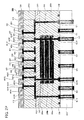
- the wiring substrate 900 relating to the present embodiment has the first resin insulating layer 200a, the base substrate 100 supporting the first resin insulating layer 200a, and the laminated capacitor 450 embedded in the first resin insulating layer 200a.
- first resin insulting layer 200a there is provided the second resin insulating layer 200b.
- second resin insulating layer 200b On the second resin insulating layer 200b there is provided the third resin insulating layer 200c.
- the upper face of the laminated capacitor 450 is at the upper face of the first resin insulating layer 200a, and the upper face of the laminated capacitor 450 and the upper face of the first resin insulating layer 200a are such that they sit flush with each other.
- the laminated capacitor 450 is such that the capacitors 350a, 350b, and 350c are laminated via the adhesive 340.
- the adhesive 340 is an insulating resin being, for example, an epoxy resin.
- the thickness of the laminated capacitor 450 is 30 ⁇ m to 100 ⁇ m, for example. It is because there is a possibility that the thickness being greater than 100 ⁇ m makes it difficult for the laminated capacitor 450 to be embedded in the first resin insulating layer 200a and alternately the thickness being less than 30 ⁇ m makes the structure to be too fine such that it could possibly impede the production efficiency of the wiring substrate.
- Each of the capacitors 350a, 350b, and 350c has the dielectric layer 330 and the plate-shaped first electrode 310 and the second electrode 320.
- the first electrode 310 and the second electrode 320 are formed of rectangular plate-shaped conductors that are identical in size.
- the first electrode 310 and the second electrode 320 are offset from each other by a predetermined distance in the direction of the plane of the electrodes, and partially overlapped.
- the first electrode 310 and the second electrode 320 are, for example, 0.2 mm to 8 mm in length, 0.1 mm to 8 mm in width, and 3 ⁇ m to 15 ⁇ m in thickness.
- the first electrode 310 and the second electrode 320 are formed of copper.
- the dielectric layer 330 is 0.5 ⁇ m to 10 ⁇ m in thickness, for example. It is because there is a possibility that the thickness of the dielectric layer 330 being less than 0.5 ⁇ m results in a poor insulation resistance of the capacitor, and, alternately, it is because there is a possibility that that of greater than 10 ⁇ m does not provide a value that would satisfy the capacitor to be of a large capacitance.
- the distance between the capacitors 350, the distance between the second electrode 320 of the capacitor 350a and the first electrode 310 of the capacitor 350b is 2 ⁇ m to 12 ⁇ m, for example.
- the thickness of the adhesive layer formed by the adhesive 340 is 2 ⁇ m to 12 ⁇ m, for example.
- it is less than 2 ⁇ m, it results in the amount of the adhesive 340 to be filled between the capacitors 350 being insufficient leading to a possibility of the adhesion between the capacitors being weak.
- the thickness of the adhesive 340 being thin could possibly lead to a low insulation resistance between the capacitors (between 350a and 350b and between 350b and 350c).
- the dielectric layer 330 is a ceramic dielectric layer.
- the dielectric layer 330 is formed of, for example, barium titanate (BaTiO 3 ).
- a thermoplastic resin or thermosetting resin containing a dielectric filler may be used for the dielectric layer 330.
- polyester may be used, and for a thermosetting resin, a phenol resin may be used.
- a dielectric filler is formed of strontium titanate (SrTiO 3 ), for example.
- the via conductors 411 electrically connect the respective first electrodes 310 mutually of the capacitors 350a, 350b, and 350c.
- the via conductors 412 electrically connect the respective second electrodes 320 mutually of the capacitors 350a, 350b, and 350c.
- conductor circuits On the base substrate 100 there are provided a plurality of conductor patters (conductor circuits) 421 (421P, 421G, 421S), and on the second resin insulating layer 200b there are provided a plurality of conductor patterns 423 (423P, 423G, 423S). On the third resin insulating layer 200c there are provided a plurality of conductor patterns 425 (425P, 425G, 425S).
- the via conductors 411 electrically connect the conductor patterns 421P and the conductor patterns 423P.
- the via conductors 412 electrically connect the conductor patterns 421G and the conductor patters 423G.
- the conductor patterns 423G connected to the via conductors 412 are connected to the ground line, and the conductor patterns 423P connected to the via conductors 411 are connected to the power supply line.
- the via conductors 441P electrically connect the conductor patterns 423P and the conductor patterns 425P.
- the via conductors 441G electrically connects the conductor patterns 423G and the conductor patterns 425G.
- the base substrate 100 is 200 ⁇ m to 800 ⁇ m in thickness.
- the base substrate 100 is formed of glass epoxy resin, for example.
- a glass epoxy resin is an epoxy resin with a glass filler added thereto which is impregnated into a glass cloth (glass epoxy substrate).
- the first resin insulating layer 200a, the second resin insulting layer 200b, and the third resin insulating layer 200c are 40 ⁇ m to 120 ⁇ m in thickness, for example.
- the resin insulating layers 200a, 200b, and 200c are made of a thermosetting resin such as an epoxy resin, for example.
- Resin insulating layers 200a, 200b and 200c may be of inorganic particulates such as glass, alumina, and barium carbonate and of a thermosetting resin.
- the glass epoxy substrate it may be a glass epoxy substrate wherein two layers of glass cloths are overlapped.
- the wiring substrate 900 is capable of performing various electrical signal processings such as transmitting electrical signals via the conductor patterns 421S, etc.
- the wiring substrate 900 is, as the laminated capacitor 450 is provided in the first resin insulating layer 200a, capable of decouple the noise while reducing the space to be used.
- the capacitor can be formed near the IC chip to be mounted on the wiring substrate 900, the delay in the power supply to the IC can be prevented.
- the laminated capacitor 450 built in the first resin insulating layer 200a is such that capacitors 350 are laminated. Accordingly, while the insulation resistance value of each of the capacitors 350 is maintained around constant by maintaining the thickness of the dielectric layer 330 of each of the capacitors 350 in a predetermined thickness and as a plurality of capacitors 350 are laminated, an increased capacitor capacitance as the laminated capacitor 450 as a whole can be achieved. Thus, a capacitor having both a large capacitance and a high insulating level can be achieved.
- the capacitors 350 are formed of the plate-shaped first electrode 310, the second electrode 320 positioned offset in the direction of the face of the electrodes off the first electrode, and the dielectric layer 330. As such, as they are alternately formed offsetting the first electrode 310 and the second electrode 320 of each of the capacitors 350, there can easily be provided the via conductors 41 electrically connecting the first electrodes 310 mutually of each of the capacitors 350a, 350b, and 350c and the via conductors 412 electrically connect one second electrode 320 to another of the second electrode 320 of each of the capacitors 350a, 350b, and 350c.
- the via conductors need not be formed in the areas where the first electrodes 310 and the second electrodes 320 are mutually opposing, the electrode areas can be made large, allowing the capacitors to be of a large capacitance to be achieved. Further, since the number of via conductors penetrating the capacitor electrodes can be small, the occurrence of cracks in the dielectric layers due to the thermal expansion of the via conductors can as best as possible be controlled.
- the laminated capacitor 450 is formed such that capacitors 350 are laminated. Accordingly, in forming the laminated capacitor 450, the insulation resistance value of each of the capacitors 350 is checked and only the capacitors 350 with a good insulation resistance are selected in advance for lamination. Thus, a non-defective item as the laminated capacitor 450 as a whole as well can be obtained to secure the insulation reliability of the laminated capacitor 450.
- a laminated capacitor to be formed such that an electrode and a dielectric layer were to be alternately laminated it would be difficult to check in advance to see if the insulation resistance of each of the capacitor portions were good. Accordingly, it would be difficult to secure the insulation reliability of the laminated capacitor at the manufacturing stage.
- the laminated capacitor 450 built in in the resin insulating layer 200a is such that the capacitors 350 are laminated with the adhesive 340 such as a resin interposed. It is also possible to use the materials with the thermal expansion coefficient of the resin used for the adhesive 340 and the thermal expansion coefficient of the resin insulating layer 200a having the same value, and, accordingly, the thermal expansion coefficient of the laminated capacitor 450 as a whole can be brought close to the thermal expansion coefficient of the resin insulating layer 200a. Thus, were the laminated capacitor 450 to heat up, the possibility of cracks occurring at the interlace between the resin insulating layer 200a and the laminated capacitor 450 is low. Thus, it is difficult for cracks to occur in the dielectric layer 330.
- a high dielectric material made of BaTiO 3 is printed in a thin film being 5 ⁇ m to 10 ⁇ m in thickness with the use of a printer such as a doctor blade to form a non-baked layer.
- a printer such as a doctor blade to form a non-baked layer.
- the sol gel process, sputtering, etc. which will be described below may be used.
- the non-baked layer is baked in vacuum in a non-oxidizing atmosphere such as N 2 gas at the temperature range of 600 to 950°C to obtain the dielectric layer 330.
- a metal layer made of copper is formed on the dielectric layer 330 with the use of a vacuum evaporation apparatus such as sputtering and, further, on this metal layer copper is added by about 5 ⁇ m by electroplating, etc., to form the second electrode 320.
- a capacitor wherein the dielectric layer 330 formed of BaTiO 3 is sandwiched by the first electrode 310 and the second electrode 320 formed of copper is obtained.
- the first electrode 310 and the second electrode 320 are formed such that they are offset in the direction of the face (i.e., the horizontal direction) by stripping the portions of the first electrode 310 and the second electrode 320 other than those needed by the etching processing with the use of cupric chloride etching solution to provide the discrete capacitors 350.
- the first electrode 310 and the second electrode 320 are offset in the horizontal direction such that the overlap of the first electrode 310 and the second electrode 320 present above and below the dielectric layer 330 is about 4 to 1.0 cm 2 .
- the alignment mark 710 is formed in the first electrode 310
- the alignment mark 720 is formed in the second electrode 320.
- capacitors 350a, 350b, and 350c are laminated in the vertical direction.
- an epoxy resin as an adhesive is interposed in between the capacitors 350.
- the discrete capacitors 350a, 350b, and 350c they are aligned with the alignment mark 710 or alignment mark 720 provided in each of the capacitors as references.
- the laminated capacitor 450 is obtained such that three capacitors 350a, 350b, and 350c are with the adhesive 340 interposed in between the capacitors.
- thermosetting resin film is attached with the use of a vacuum laminator under the lamination conditions of the temperature being 50 through 170°C and the pressure being 0.4 through 1.5 MPa.
- conductor patterns 421 421P, 421G, 421S.
- the base substrate 100 is a glass epoxy substrate having a thickness of 0.6 mm. While the thermosetting resin film is semi-cured when it is attached, it becomes the first resin insulating layer (the lower resin insulating layer) 200a as it hardens.
- a resin film two sheets of ABF-45SH made by Ajinomoto Co., Inc., can be used.
- the laminated capacitor 450 is aligned on the first resin insulating layer 200a which is semi-hardened and laminated.
- the alignment of the two is performed such that the alignment mark 710 present in the capacitor 350a from among the capacitors of the laminated capacitor 450 and the alignment mark 730 of the base substrate 100 are recognized by a camera.
- it is performed such that the alignment mark 720 present in the capacitor 350c from among the capacitors of the laminated capacitor 450 and the alignment mark 730 in the base substrate 100 are recognized by a camera. It may be either that either one of the alignment mark 710 and the alignment mark 720 may be provided or that the both may be provided.
- the laminated capacitor 450 is embedded into the resin insulting layer 200a and concurrently that the first resin insulating layer 200a is cured.
- the laminated capacitor 450 is embedded in the first resin insulating layer 200a such that the upper face of the laminated capacitor 450 and the upper face of the first resin insulating layer 200a sit flush with each other.
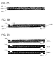
- the laminated capacitor it is possibly for the laminated capacitor to be laminated on the first resin insulating layer 200a such, as illustrated in FIG. 2H , that a portion of the capacitor 350c is embedded.
- the alignment mark 720 provided on the capacitor 350c or the alignment mark 710 provided in the capacitor 350a of the laminated capacitor 450 and the alignment mark 730 provided on the base substrate 100 are the reference marks for aligning the laminated capacitor 450 and the first resin insulating layer 200a.
- a resin film is attached with the use of a vacuum laminator under the lamination conditions of the temperature being 50-170°C and the pressure being 0.4 to 1.5 MPa.
- ABF-45SH made by Ajinomoto Co., Inc., for example, can be used.
- the resin film is thermally treated at 170°C for two hours such that it is cured to form the second resin insulating layer (the upper resin insulating layer) 200b.
- the through holes 470 (470P, 470G, 470S) are provided penetrating the second resin insulating layer 200b, the first resin insulating layer 200a, and the laminated capacitor 450 and reaching the conductor patterns 421 (the conductor patterns for power supply 421P, the conductor patterns for ground 421G, the conductor patterns for signal 421S) on the base substrate 100.
- the through holes 470P are the through holes for power supply reaching the conductor patterns for power supply 421P.
- the through holes 470G are the through holes for ground reaching the conductor patterns for ground 421G.
- the diameters of the through holes 470 (470P, 470G, 470S) are 20 ⁇ m to 100 ⁇ m. It is possibly to provide the through holes 470 (470P, 470G, 470S) not with a carbon dioxide gas laser but with a drill.
- the positions of the through holes 470 are determined by recognizing either of the alignment mark 730 of the base substrate 100, the alignment mark 710 of the capacitor 350a in the laminated capacitor 450, or the alignment mark 720 of the capacitor 350c in the laminated capacitor 450 with a camera or an X-ray.
- capacitors are formed with the portion where the first electrode 310 and the second electrode 320 overlap.
- the first electrode 310 and the second electrode 320 it is possible for the first electrode 310 and the second electrode 320 to be offset only in the lateral direction, and, as illustrated in FIG. 2L , it is possible for the first electrode 310 and the second electrode 320 to be offset in the lateral direction and in the longitudinal direction.
- the portion where the first electrode 310 and the second electrode 320 overlap is illustrated by oblique lines.
- the first electrode 310 and the second electrode 320 are offset from each other in the direction of the face such that there are present portions where they do not overlap. In the portions where they do not overlap there are formed the through holes 470P and 470G.
- the through holes 470P and 470G since in the portion where the first electrode 310 and the second electrode 320 mutually oppose there are not formed the through holes 470P and 470G, the area where the first electrode 310 and the second electrode 320 mutually oppose can be made large. While the through holes for power supply 470P are in contact with the first electrode 310 (the electrode for power supply), they are not in contact with the second electrode 320 (the electrode for ground). While the through holes for ground 470G are in contact with the second electrode 320, they are not in contact with the first electrode 310.
- the through holes for signal 470S reaching the conductor patterns for signal.
- the through holes for signal 470S are formed in the area where the laminated capacitor 450 is not present.
- a surface treatment is performed on the surface of the second resin insulating layer 200b by a catalyst.
- electroless plated films electroless copper-plated films
- electroplated films electroplated films (electro-copper-plated films).
- an etching resist is formed on the electroplated films.
- the etching resist is patterned. The photolithography method whereby the portions where patterns are formed on a resin layer and the portions where the through-hole plating is protected are covered with resists is referred to as a renting process.
- the conductor patterns 423 (the conductor pattern for power supply 423P, the conductor pattern for ground 423G, the conductor pattern for signal 423S) and the via conductors 411, 412, 413 are formed.
- the via conductors 411 are via conductors for power supply, electrically connecting, as illustrated in FIG. 2M , the first electrodes 310 mutually of the capacitor 350a, the capacitor 350b, and the capacitor 350c.
- the via conductors 412 are via conductors for ground, electrically connecting, as illustrated in FIG. 2M , one second electrode to another of the second electrodes 320 of the capacitor 350a, the capacitor 350b, and the capacitor 350c.
- the via conductors for power supply 411 connect the conductor patterns for power supply 421P on the base substrate 100 and the conductor patterns for power supply 423P on the second resin insulating layer 200b.
- the via conductors for ground 412 connect the conductor patterns for ground 421G on the base substrate 100 and the conductor patterns for ground 423G on the second resin insulating layer 200b.
- the third resin insulating layer 200c As illustrated in FIG. 2N , on the second resin insulting layer 200b and the conductor patterns 423 (423P, 423G, 423S) there is formed the third resin insulating layer 200c.
- the material for the third resin insulating layer 200c is the same as those of the second resin insulating layer 200b and the first resin insulating layer 200a.
- the third resin insulating layer 200c there are formed through holes with a carbon dioxide gas laser. It is possible to form through holes with a drill.
- a surface treatment is performed on the surface of the third resin insulating layer 200c by a catalyst. Following the surface treatment by a catalyst, an electroless plated film is formed on the surface of the substrate. Subsequently, a plated resist is formed on the electroless plated film. Following that, the plated resist is treated with exposure and development to pattern the plated resist. And, on the areas where the plated resist is not formed there are formed electro-plated films. After the plated resist is stripped, there are provided, as illustrated in FIG.
- the outermost conductor patterns 425 (the outermost conductor patterns for power supply 425P, the outermost conductor patterns for ground 425G, the outermost conductor patterns for signal 425S) made of electroless plated film and electro-plated film provided on said electroless plated film by removing the electroless plated film between the electroplated films.
- solder resist 700 is formed on the third resin insulating layer 200c and the outermost conductor patterns 425 (425P, 425G, 425S).
- opening portions are provided in the solder resist 700 to expose portions of the conductor patterns 425 (425P, 425G, 425S) such that the pads 427 (the pads for power supply (the first eternal terminals) 427P, the pads for ground (the second external terminals) 427G, the pads for signal 427S) are formed.
- the portions exposed from the opening portions constitute the pads 427 (427P, 427G, 427S).
- the first electrodes 310 and the pads for power supply 427P are connected via the via conductors 411, the conductor patterns 423P, and the via conductors 441P.
- the second electrodes 320 and the pads for ground 427G are connected via the via conductors 412, the conductor patterns 423G, and the via conductors 441G.
- metal films films made of Ni, Au, Pd, Ag, Pt, etc., for example, can be formed.
- Ni film, Pd film, and Au film are formed in that order.
- the metal films may be of one layer or of a plurality of metal films. To illustrate, Ni film and Au film can be formed on the pads in that order.
- solder paste is printed. Subsequently, it is reflowed to provide the solder bumps 429 such that the wiring substrate 900 illustrated in FIG. 1 is obtained.
- the IC chip 800 is mounted via the solder bumps 429, as illustrated in FIG. 2Q .
- the resin insulating layers, conductors patterns, and the via conductors are formed on only one face of the base substrate 100, it is possible to form the resin insulating layers, the conductor patterns, and the via conductors on both faces of the base substrate 100, as illustrated in FIG. 2R .
- the surfaces of the resin insulting layers 200a, 200b, 200c, the surfaces of the conductor patterns 421, 423, 425, the surfaces of the first electrodes 310, and the surfaces of the second electrodes 320 are roughened.
- the distance between the laminated capacitor 450 and the IC chip 800 is short.
- the resin insulating layers 200 consisted of the first resin insulating layer 200a, the second resin insulating layer 200b, and the third resin insulating layer 200c.
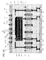
- the wiring substrate 900 relating to the second embodiment differs from that of the first embodiment as illustrated in FIG. 3 such that the resin insulating layers 200 consist of the first resin insulating layer 200a and the second resin insulating layer 200b.
- the electrode positioned at the uppermost layer of the laminated capacitor 450 is formed such that the first electrode 310 of the capacitor 350a and the conductor patterns for power supply 423P on said first electrode 310 are integrated. Accordingly, in the wiring substrate 900 relating to the second embodiment, the thickness of the electrode present on the surface layer of the laminated capacitor 450 is thicker than the wiring substrate 900 relating to the first embodiment. Accordingly, the rigidity of the laminated capacitor 450 is enhanced. Thus, the dielectric layer of the laminated capacitor 450 is less susceptible to the occurrence of cracks.
- the pads for power supply (the first external terminals) 427P and the first electrode 310 of each of the capacitors 350a, 350b, and 350c are electrically connected via the via conductors 441P, the conductor patterns 423P, and the via conductors 411.
- the pads for ground (the second external terminals) 427G and the second electrode 320 of each of the capacitors 350a, 350b, and 350c are electrically connected via the via conductors 441G, the conductor patterns 423G, and the via conductors 412.
- the outermost conductor patterns for power supply 425P On the second resin insulating layer 200b there are provided the outermost conductor patterns for power supply 425P, the outermost conductor patterns for ground 425G, and the outermost conductor patterns for signal 425S.
- Opening portions are provided in the solder resist 700 to expose portions of the conductor patterns 425 (425P, 425G, 425S) such that the pads 427 (the pads for power supply (the first external terminals) 427P, the pads for ground (the second external terminals) 427G, the pads for signal 427S) are formed.
- the through holes 470 reaching the conductor patterns for power supply on the core substrate, the through holes 470G reaching the conductor patterns for ground on the core substrate, the through holes 470S reaching the conductor patterns for signal on the core substrate. While in the manufacturing method relating to the first embodiment, through holes were concurrently formed in the second resin insulating layer 200b as well, since in the manufacturing method relating to the present embodiment, it is only that through holes are formed penetrating the laminated capacitor 450 and the first resin insulating layer 200a, it results in an easy hole processing and an improved yield. And, a surface treatment is performed by a catalyst on the surface of the first resin insulating layer 200a in which the through holes 470 are formed.
- the via conductors for ground 412, the via conductors for power supply 411, the via conductors for signal 413, and the conductor patterns 423 are formed with the tenting process.
- the electrode positioned at the uppermost layer of the laminated capacitor 450 is formed such that the first electrode 310 of the capacitor 350a and the conductor patterns for power supply 423P on said first electrode 310 are integrated.
- the electrode positioned at the uppermost layer of the laminated capacitor 450 refers to the electrode at the surface layer of the capacitor 450 positioned on the side close to the IC chip 800 to be mounted.
- the conductor patterns for power supply 423P on the first electrode 310 are formed of an electroless plated film and an electroplated films on said electroless plated film.
- the via conductors 412 connect the second electrodes 320 mutually of the capacitor 350a, the capacitor 350b, and the capacitor 350c. And, the via conductors 412 connect the conductor patterns for ground 421G on the base substrate 100 and the conductor patterns for ground 423G on the first resin insulting layer 200a.
- the via conductors 411 connect the first electrodes 310 mutually of the capacitor 350a, the capacitor 350b, and the capacitor 350c. And, the via conductors 411 connect the conductor patterns for power supply 421P on the base substrate 100 and the conductor patterns for power supply 423P on the first resin insulting layer 200a.
- the second resin insulating layer 200b On the first resin insulting layer 200a, the laminated capacitor 450, and the conductor patterns 423 (423P, 423G, 423S) there is formed the second resin insulating layer 200b. And, in the second resin insulating layer 200b there are formed through holes. And, a surface treatment is performed with a catalyst on the surface of the substrate in which through holes are formed.
- the solder resist 700, the pads 427, and the solder bumps 429 are formed to obtain the wiring substrate 900 illustrated in FIG. 3 .
- the wiring substrate 900 it is possible to manufacture the wiring substrate 900 at an easy cost since it can be manufactured with one less resin insulating layer as compared to the first embodiment.
- the resin insulating layers, conductors patterns, and the via conductors are formed on only one face of the base substrate 100, it is possible to form the resin insulating layers, the conductor patterns, and the via conductors on both faces of the base substrate 100, as illustrated in FIG. 4D .
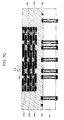
- the third embodiment will be illustrated in FIG. 5 .
- the first electrodes 310 and the second electrodes 320 are not offset from each other in the direction of the face, unlike the first embodiment.
- the first electrodes 310 there are provided a plurality of the first opening portions 311, and in the second electrodes 320 there are provided a plurality of the second opening portions 322.
- a plurality of the first via conductors 411 electrically connect the first electrodes 310 mutually while running through the second opening portions 322 without being in contact with the second electrodes 320.
- a plurality of the second via conductors 412 electrically connect one second electrode to another of the second electrodes 320 while running through the first opening portions 311 without being in contact with the first electrodes 310.
- a plurality of the first via conductors 411 and a plurality of the second via conductors 412 penetrate the laminated capacitor 450. Accordingly, in the wiring substrate 900 relating to the third embodiment, it is possible for a plurality of the first via conductors 411 and a plurality of the second via conductors 412 to control the deformation of the adhesive 340 such that the anti-crack property of the laminated capacitor 450 is likely to be improved.
- the via conductors for power supply 411 and the via conductors for ground 412 are disposed in a grid pattern or lattice pattern.
- the distances between adjacent via conductors for power supply 411 are roughly the same.
- the distances between adjacent via conductors for ground 412 are roughly the same.
- a capacitor 350 comprising the first electrode 310, the second electrode 320, and the dielectric layer 330 sandwiched between the first electrode 310 and the second electrode 320 is formed.
- the capacitor 350 is formed likewise as with the first embodiment.
- FIG. 7B in FIG. 7C being a plan view viewing the capacitor 350 from the first electrode 310 side, and in FIG. 7D being a plan view viewing the capacitor 350 from the second electrode 320 side, the first electrode 310 and the second electrode 320 are patterned. At this time, the alignment marks 710 and 720 are concurrently formed.
- first electrode 310 there are formed the opening portions 311 and inside the opening portions 311 thereof there are formed via conductors for ground 412. The first electrode 310 and the via conductors for ground 412 are not in contact.
- second electrode 320 there are formed the opening portions 322, and inside the opening portions 322 thereof there are formed via conductors for power supply 411. The second electrode 320 and the via conductors for power supply 411 are not in contact.
- capacitors 350 obtained by the preceding step are prepared, and laminated via the adhesive 340.
- the capacitors 350a, 350b, and 350c are aligned based on the alignment marks 710, 720 of each of the capacitors 350.
- the laminated capacitor 450 comprising the capacitors 350a, 350b, 350c and the adhesive 340 disposed in between each of the capacitors is formed.
- the laminated capacitor 450 is formed with a vacuum press.
- the conditions for the vacuum press are the temperatures being 50 to 170°C and the pressure being 0.4 to 1.5 MPa.
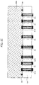
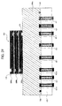
- the opening portions 311 of each of the capacitors constituting the laminated capacitor 450 are formed at nearly the same positions in the sectional direction such that the first electrodes 310 and the second electrodes 320 are not short-circuited by the via conductors 412 penetrating the laminated capacitor 450. Namely, as illustrated in FIG. 7F , the opening portions 311 formed in the capacitors 350a, 350b, 350c are provided at the positions that overlap each other in the sectional direction.
- the opening portions 322 of each of the capacitors constituting the laminated capacitor 450 are formed at nearly the same positions in the sectional direction such that the first electrodes 310 and the second electrodes 320 are not short-circuited by the via conductors 411 penetrating the laminated capacitor 450. Namely, in FIG. 7F , the opening portions 322 formed in the capacitors 350a, 350b, 350c are provided at the positions that overlap each other in the sectional direction.
- the laminated capacitor 450 is embedded in the first resin insulating layer 200a.
- the through holes 470 (470P, 470G, 470S) are formed.
- the through holes 470 (470P, 470G, 470S) run through the laminated capacitor 450 and the first resin insulating layer 200a, and reach the conductor patterns 421 (421P, 421G, 421S) of the base substrate 100.
- the positions for the through holes 470 (470P, 470G, 470S) to be formed at they are formed by the laser processing with one of the alignment mark 730 of the base substrate 100 and the alignment marks 710, 720 formed on the laminated capacitor 450 as the basis.
- the through holes for power supply 470P run through the first electrodes 310 and the dielectric layers 330. And, the through holes for power supply 470P are formed inside the opening portions 322 of the second electrodes 320, and not in contact with the inside walls of the opening portions 322.
- the through holes for ground 470G run through the second electrodes 320 and the dielectric layers 330. And, the through holes for ground 470G are formed inside the opening portions 311 of the first electrodes 310, and not in contact with the inside walls of the opening portions 311.
- the via conductors for ground 412, the via conductors for power supply 411, the via conductors for signal 413, and the conductor patterns 423 are formed with the tenting process.
- the conductor patterns 423 (the conductor patterns for power supply 423P, the conductor patterns for ground 423G, the conductor patterns for signal 423S) comprise electroless plated fams and electroplated films on said electroless plated films.
- the uppermost layer electrode of the laminated capacitor 450 is formed such that the first electrode 310 of the capacitor 350a and the conductor patterns for power supply 423P (the electroless plated films on the first electrode 310 and the electroplated films on said electroless plated films) are integrated.
- the uppermost layer electrode of the laminated capacitor 450 refers to the surface layer electrode being of the laminated capacitor 450 being positioned at the close side to the IC chip to be mounted.
- the wiring substrate 900 as being illustrated in FIG. 5 is obtained via the steps being illustrated in FIG. 4C and FIG. 4D .
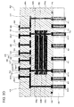
- the wiring substrate 900 relating to the fourth embodiment in accordance with the present invention is illustrated in FIG. 8 .
- the wiring substrate 900 relating to the fourth embodiment is such, unlike the wiring substrate 900 relating to the first embodiment, that the base substrate (core substrate) 100 having a core material such as glass cloth and fiber glass is not provided. Accordingly, all the insulating layers can be resin insulating layers (resin films). Thus, the capacitor substrate with a built-in capacitor can be made thin.
- the distance between the external power supply and the laminated capacitor 450 built-in in the wiring substrate 900 and the distance between the chip capacitor (a drawing omitted) mounted on the surface of the wiring substrate 900 and the laminated capacitor 450 can be made short.
- the support board 150 is prepared.
- the support board 150 is a copper board, for example. It is possible to use, other than copper, a metal board such as a nickel board, an aluminum board, and an iron board for the support board 150 material.
- the plated resist 160 is formed on the support board 150.
- a plurality of opening portions are provided in the plated resist 160 by the plated resist 160 being patterned with the exposure and development steps.
- the opening portions provided in the plated resist 160 are electroplated with the gold-plated film 911, the nickel-plated film 912, and the copper-plated film 913 in that order, and there are formed the first external connection terminals 600 (the external terminals for power supply (the first external terminals) 600P, the external terminals for ground (the second external terminals) 600G, the external terminals for signal 600S).
- the alignment mark (the first alignment mark) 621 is formed on the support board 150 there is formed the alignment mark (the first alignment mark) 621. It is possible to form a palladium film between the gold-plated film 911 and the nickel-plated film 912.
- the plated resist 160 is stripped and the resin film (the first lower resin insulating layer) 400d is formed.
- This first lower resin insulating layer (the lowest layer resin insulation) 400d is present, as illustrated in FIG. 8 , below the first resin insulating layer 400a having the laminated capacitor 450 built-in.
- the first external connection terminals 600 600P, 600G, 600S
- the surfaces of the first external connection terminals 600 are positioned on nearly the same plane as the first face of the lowermost resin insulating layer.
- the first conductor patterns 610 (the first conductor patterns for power supply 610P, the first conductor patterns for ground 610G, the first conductor patterns for signal 610S) are formed with the semi-additive process on the upper face of the first lower resin insulating layer 400d (the opposite face from the face on which the external terminals are formed).
- the first via conductors 611 (the first via conductors for power supply 611P, the first via conductors for ground 611G, the first via conductors for signal 611S) are formed connecting the first external connection terminals 600 (600P, 600G, 600S) and the first conductor patterns 610 (610P, 610G, 610S).
- the second alignment mark 622 is concurrently formed.
- the first via conductors for power supply 611P connect the external terminals for power supply 600P on the first face side (the first external terminals for power supply) and the first conductor patterns for power supply 610P.
- the first via conductors for ground 611G (the first external terminals for ground) connect the external terminals for ground 600G on the first face side and the first conductor patterns for ground 610G.
- the first via conductors for signal 611S (the first external terminals for signal) connect the external terminals for signal 600S on the first face side and the first conductor patterns for signal 610S.
- the first conductor patterns 610 (610P, 610G, 610S) and the first lower resin insulating layer 400d there is formed a resin film (the first resin insulating layer 400a) having the first face and the second face being on the opposite side from the first face.
- the first resin insulating layer 400a two sheets of ABF-45SH made by Ajinomoto Co., Inc., are overlapped which can be laminated.
- the laminated capacitor 450 is laminated on the first resin insulating layer 400a such that they are aligned.
- the lamination position of the laminated capacitor 450 can be determined using the second alignment mark 622 formed on the first resin insulating layer 400a and the alignment mark 720 of the laminated capacitor 450, for example.
- the laminated capacitor 450 can be formed by the manufacturing method which is the same as that of the first embodiment.
- the laminated capacitor 450 is embedded on the second face side of the first resin insulating layer 400a.
- the surface of the first electrode 310 of the capacitor 350a and the second face of the first resin insulating layer 400a are disposed on nearly the same plane.
- the method of embedding the laminated capacitor 450 is the same as the method described with FIG. 2G .
- the via conductors (the second via conductors) 651 (the second via conductors for power supply 651P, the second via conductors for ground 651G, the second via conductors for signal 651S) are formed.
- the second conductor patterns 650 (the second conductor patterns for power supply 650P, the second conductor patterns for ground 650G, the second conductor patterns for signal 650S) are formed.
- the second via conductors for power supply 651P connect one first electrode 310 to another of the first electrodes 310 of each of the capacitors 350a, 350b, 350c of the laminated capacitor 450. Further, the via conductors 651P connect the second conductor patterns for power supply 650P and the first conductor patterns for power supply 610P.
- the second via conductors for ground 651G connect the second electrodes 320 mutually of each of the capacitors 350a, 350b, 350c of the laminated capacitor 450. Further, the via conductors 651G connect the second conductor patterns for ground 650G and the first conductor patterns for ground 610G.
- the via conductors for signal 651S connect the second conductor patterns for signal 650S and the first conductor patterns for signal 610S.
- the first electrodes 310 of each of the capacitors 350a, 350b, 350c and the first external terminals 600P are electrically connected.
- the second electrodes 320 of each of the capacitors 350a, 350b, 350c and the second external terminals 600G are electrically connected.
- the third conductor patterns 660 (the third conductor patterns for power supply 660P, the third conductor patterns for ground 660G, the third conductor patterns for signal 660S).
- the third via conductors 661 (the third via conductors for power supply 661P, the third via conductors for ground 661G, the third via conductors for signal 661S) connecting the second conductor patterns 650 (650P, 650G, 650S) and the third conductor patterns 660 (660P, 660G, 660S) are formed.
- the third via conductors for power supply 661P connect the third conductor patterns for power supply 660P and the second conductor patterns for power supply 650P.
- the third via conductors for ground 661G connect the third conductor patterns for ground 660G and the second conductor patterns for ground 650G.
- the third via conductors for signal 661S connect the second conductor patterns for signal 650S and the third conductor patterns for signal 660S. These connections can be formed with the semi-additive process, for example.
- solder resist 700 As illustrated in FIG. 9P , on the second resin insulating layer 400b and the third conductor patterns 660 (660P, 660G, 660S) there is formed the solder resist 700.
- FIG. 9Q there are provided a plurality of opening portions in the solder resist 700. Those opening portions partially open up the third conductor patterns 660 (660P, 660G, 660S).
- the second external connection terminals 670 are formed on the second resin insulating layer (the uppermost resin insulating layer) 400b, comprising the second external connection terminals for power supply (the third external terminals) 670P, the second external connection terminals for ground (the fourth external terminals) 670G, and the second external connection terminals for signal 670P.
- the metal film may be of one layer of a gold-plated layer and of two layers of a nickel-plated layer and a gold-plated layer on the nickel-plated layer.
- the support board 150 is etch-removed with a cupric chloride etching solution.
- the support board 150 can be removed without the external connection terminals being etch-removed on account of metal films being formed on the second external connection terminals 670 (670P, 670G, 670S) and the first external connection terminals 600 (600P, 600G, 600S).
- the removal of the support board 150 exposes the external terminal faces (the exposed portions of the metal films) of the first external connection terminals 600.
- the wiring substrate 900 illustrated in FIG. 8 is obtained by the second solder bumps being formed on the external terminal faces (the exposed portions of the metal films) of the second external connection terminals 670 (670P, 670G, 670S) and by the first solder bumps being formed on the external terminal faces of the first external connection terminals 600 (600P, 600G, 600S).
- An electronic device such as an IC chip may be loaded via the first solder bumps. It may be connected to another substrate (a motherboard) via the second solder bumps. And, while in FIG. 8 solder bumps are formed on the external terminal faces of the first external connection terminals 600 and on the external terminal faces of the second external connection terminals 670, it may be that the solder bumps on the outer terminal faces of the second external connection terminals 670 and conductive pins are loaded (mounted) on the external terminal faces of the first external connection terminals 600 via soldering. It may be that the solder bumps on the outer terminal faces of the first external connection terminals 600 and conductive pins are loaded (mounted) on the external terminal faces of the second external connection terminals 670 via soldering.
- the IC chip may be loaded on the upper face side or the lower face side of the wiring board, it is preferred that the IC chip be loaded on the surface of the substrate with a built-in capacitor on the side where the distance between the external terminals and the capacitor is short (the distance in the sectional direction of the substrate).
- the resin insulating layer (the resin film) is of three layers, it is possible for it to be multi-layered with four layers or more by repeating the steps of FIG. 9M through FIG. 9O .
- solder resist having opening portions allowing the first external connection terminals 600 (600P, 600G, 600S) to be exposed.
- the wiring substrate 900 illustrated in FIG. 10 is, unlike the wiring substrate 900 illustrated in FIG. 8 , an example wherein the first external connection terminals 600 and the laminated capacitor 450 are embedded in the same resin insulating layer.
- the wiring substrate 900 illustrated in FIG. 10 is of the two-layer structure with the first resin insulating layer (the lowermost resin insulating layer) 400a having the first face and the second face being on the opposite side from the first face and the second resin insulating layer (the uppermost resin insulating layer) 400b having the first face and the second face being on the opposite side from the first face.
- the laminated capacitor 450 In the second face side of the first resin insulating layer 400a there is embedded the laminated capacitor 450.
- the surface of the first electrode 310 of the capacitor 350a and the second face of the lowermost resin insulating layer 400a are disposed on nearly the same plane.
- the first face side (the first surface of the wiring board 900) of the first resin insulating layer 400a there are embedded the first external connection terminals 600.
- the surfaces of the first external connection terminals 600 and the first face of the lowermost resin insulating layer 400a are disposed on nearly the same plane.
- the second external connection terminals 670 comprising the second external connection terminals for power supply (the third external terminals) 670P, the second external connection terminals for ground (the fourth external terminals) 670G, and the second external connection terminals for signal 670P. And, in the second resin insulating layer 400b there are formed via conductors.
- the method of manufacturing the wiring board 900 illustrated in FIG. 10 first undertakes the steps illustrated in FIG. 9A through FIG. 9E . Subsequently, it undertakes the steps illustrated in FIG. 9I through FIG. 9R , the plating resist 160 being removed and the first solder bumps being formed on the first external connection terminals 600 (600P, 600G, 600S) to obtain the wiring substrate 900 illustrated in FIG. 10 .
- the printed wiring board in accordance with the fourth embodiment may, as with the third embodiment, have a laminated capacitor built in wherein the capacitors wherein the first electrodes and the second electrodes not being offset in the direction of the face are laminated with an adhesive.
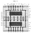
- the wiring board 900 relating to the fifth embodiment in accordance with the present invention is such, unlike the wiring board 900 relating to the first embodiment, that there are provided the resin insulating layer 200a on and the lower resin insulating layer 270d underneath the base substrate 100 as shown in FIG. 11 . And, in the resin insulating layer 200a there is embedded the laminated capacitor 450a, and in the lower resin insulating layer 270d there is embedded the laminated capacitor 450b.
- the constitution as such allows not only a reduction in noise on the base substrate 100 but also a reduction in noise also underneath the base substrate 100 to be effectively worked out.
- this wiring substrate 900 it is possible, following FIG. 2Q , for example, for the lower resin insulating layer 270d to be provided on the lower face of the base substrate 100 and that the laminated capacitor 450b is embedded in that lower resin insulating layer 270d such that it is formed.
- the laminated capacitor 450 was formed such that three capacitors 350a, 350b, 350c were laminated. Naturally, it is not limited to this.
- the laminated capacitor 450 can be such that two or four to thirty or more capacitors, for example, are laminated with the adhesive 340 interposed.
- the dielectric layer 330 was formed of barium titanate (BaTiO 3 ). Naturally, it is not limited to this. It is possible to use for the dielectric layer 330 any or a mixture of strontium titanate (SrTiO 3 ), tantalum oxide (TaO 3 , Ta 2 O 5 ), lead zirconate titanate (PZT), lead lanthanum zirconate titanate (PLZT), lead niobium zirconate titanate (PNZT), lead calcium zirconate titanate (PCZT), and lead strontium zirconate titanate (PSZT).
- strontium titanate SrTiO 3
- tantalum oxide TaO 3 , Ta 2 O 5
- PZT lead zirconate titanate
- PZT lead lanthanum zirconate titanate
- PNZT lead niobium zirconate titanate
- PCZT lead calcium zirconate titanate
- PSZT lead strontium zirconate
- strontium titanate (SrTiO 3 ) was used as a dielectric filler.
- a dielectric filler it is possible to use, for example, calcium titanate (CaTiO 3 ), magnesium titanate (Mg 2 TiO 3 ), neodymium titanate (Nd 2 Ti 2 O 7 ), etc.
- epoxy resins were used for resins constituting resin insulating layers (resin films). Naturally, this is not limited to this.
- a resin constituting a resin insulating layer polyimide, polycarbonate, denatured polyphenylene ether, polyphenylene oxide, polybutylene terephthalate, polyacrylate, polysulfone, polyphenylenesulfide, polyetheretherketone, polysalfone, polyethersalfone, polyphenysalfone, polyphtalamide, polyamideimide, polyketone, polyacetal, etc., for example, alone or a combination thereof with an epoxy resin may be used.
- copper was used as a metal constituting the first electrode 310 and the second electrode 320.
- a metal constituting the first electrode 310 and the second electrode 320 platinum, gold, nickel, tin, silver, etc., for example, alone or a mixture thereof may be used. Further, it is possible to use a different kind of metal for the first electrode 310 and the second electrode 320 each.
- a capacitor was formed such that on the first electrode 310 made of copper there was printed a high dielectric material which was baked to form a dielectric layer 330 and subsequently that a metal layer made of copper was formed on the dielectric layer 330 with the use of a vacuum evaporation apparatus such as sputtering, etc.
- a vacuum evaporation apparatus such as sputtering, etc.
- diethoxy barium and titanium bitetraisopropoxide are dissolved in a mixture solvent of dehydrated methanol and 2-methoxy ethanol, which is stirred for three days under nitrogen atmosphere at room temperature to adjust a alkoxide precursor composition solution of barium and titanium.
- this precursor composition solution being stirred while being maintained at 0°C, water which has in advance been decarboxylated is sprayed under a nitrogen flow at the rate of 0.5 microliter/minute for hydrolysis.
- the sol gel solution prepared as such is passed through a filter such that a precipitate, etc., are filtered.
- the filtrate obtained is spin-coated onto the first electrode 310 made of copper being 12 ⁇ m in thickness. Subsequently, it is inserted into an electric furnace maintained at 850°C and baked to obtain the dielectric layer 330.
- a copper layer is formed on the dielectric layer 330 with the use of a vacuum evaporation apparatus such as sputtering, etc., and, further, copper is added onto this copper layer by about 10 ⁇ m by electroplating, etc., to obtain the second electrode 320.
- the present invention can be used for a wiring board with built-in capacitors with a high capacitance and the insulation resistance secured.
Landscapes
- Engineering & Computer Science (AREA)
- Microelectronics & Electronic Packaging (AREA)
- Power Engineering (AREA)
- Manufacturing & Machinery (AREA)
- Production Of Multi-Layered Print Wiring Board (AREA)
- Fixed Capacitors And Capacitor Manufacturing Machines (AREA)
- Ceramic Capacitors (AREA)
- Parts Printed On Printed Circuit Boards (AREA)
Applications Claiming Priority (2)
| Application Number | Priority Date | Filing Date | Title |
|---|---|---|---|
| US98096907P | 2007-10-18 | 2007-10-18 | |
| EP07831157A EP2091311B1 (fr) | 2007-10-18 | 2007-11-02 | Panneau de câblage et son procédé de fabrication |
Related Parent Applications (1)
| Application Number | Title | Priority Date | Filing Date |
|---|---|---|---|
| EP07831157.8 Division | 2007-11-02 |
Publications (1)
| Publication Number | Publication Date |
|---|---|
| EP2217045A1 true EP2217045A1 (fr) | 2010-08-11 |
Family
ID=40567120
Family Applications (2)
| Application Number | Title | Priority Date | Filing Date |
|---|---|---|---|
| EP10162269A Withdrawn EP2217045A1 (fr) | 2007-10-18 | 2007-11-02 | Substrat de câblage et son procédé de fabrication |
| EP07831157A Active EP2091311B1 (fr) | 2007-10-18 | 2007-11-02 | Panneau de câblage et son procédé de fabrication |
Family Applications After (1)
| Application Number | Title | Priority Date | Filing Date |
|---|---|---|---|
| EP07831157A Active EP2091311B1 (fr) | 2007-10-18 | 2007-11-02 | Panneau de câblage et son procédé de fabrication |
Country Status (7)
| Country | Link |
|---|---|
| US (1) | US8148645B2 (fr) |
| EP (2) | EP2217045A1 (fr) |
| JP (1) | JP4773531B2 (fr) |
| KR (1) | KR101085322B1 (fr) |
| CN (1) | CN101502191B (fr) |
| TW (1) | TWI365688B (fr) |
| WO (1) | WO2009050829A1 (fr) |
Families Citing this family (21)
| Publication number | Priority date | Publication date | Assignee | Title |
|---|---|---|---|---|
| US20090296310A1 (en) * | 2008-06-03 | 2009-12-03 | Azuma Chikara | Chip capacitor precursors, packaged semiconductors, and assembly method for converting the precursors to capacitors |
| WO2010041589A1 (fr) * | 2008-10-08 | 2010-04-15 | 株式会社村田製作所 | Module composite |
| EP2410827B1 (fr) * | 2009-03-19 | 2018-09-19 | Murata Manufacturing Co., Ltd. | Circuit imprimé et corps mère laminé |
| JP5589314B2 (ja) * | 2009-06-25 | 2014-09-17 | 株式会社リコー | 電子部品モジュールの製造方法 |
| EP2519089B1 (fr) * | 2009-12-24 | 2017-09-13 | Murata Manufacturing Co., Ltd. | Module de circuits |
| CN103782665B (zh) * | 2011-08-15 | 2017-04-26 | 艾思玛太阳能技术股份公司 | 在电路板的支持物中包括电容器的电子设备及其生产方法 |
| CN103096646B (zh) * | 2011-10-31 | 2016-01-20 | 健鼎(无锡)电子有限公司 | 内埋元件的多层基板的制造方法 |
| US20140070404A1 (en) * | 2012-09-12 | 2014-03-13 | Shing-Ren Sheu | Semiconductor package structure and interposer therefor |
| US9035194B2 (en) * | 2012-10-30 | 2015-05-19 | Intel Corporation | Circuit board with integrated passive devices |
| KR101420526B1 (ko) * | 2012-11-29 | 2014-07-17 | 삼성전기주식회사 | 전자부품 내장기판 및 그 제조방법 |
| US20140167900A1 (en) | 2012-12-14 | 2014-06-19 | Gregorio R. Murtagian | Surface-mount inductor structures for forming one or more inductors with substrate traces |
| JP6649770B2 (ja) * | 2014-02-21 | 2020-02-19 | 三井金属鉱業株式会社 | 内蔵キャパシタ層形成用銅張積層板、多層プリント配線板及び多層プリント配線板の製造方法 |
| US20190045620A1 (en) * | 2014-07-09 | 2019-02-07 | Schreiner Group Gmbh & Co. Kg | Sensor device with a flexible electrical conductor structure |
| US20160055976A1 (en) * | 2014-08-25 | 2016-02-25 | Qualcomm Incorporated | Package substrates including embedded capacitors |
| US9659850B2 (en) * | 2014-12-08 | 2017-05-23 | Qualcomm Incorporated | Package substrate comprising capacitor, redistribution layer and discrete coaxial connection |
| CN104900406B (zh) * | 2015-06-01 | 2017-10-10 | 中国科学院上海硅酸盐研究所 | 可键合多层陶瓷电容器及其制备方法 |
| JP6741419B2 (ja) * | 2015-12-11 | 2020-08-19 | 株式会社アムコー・テクノロジー・ジャパン | 半導体パッケージおよびその製造方法 |
| US10373904B2 (en) | 2017-08-28 | 2019-08-06 | Micron Technology, Inc. | Semiconductor devices including capacitors, related electronic systems, and related methods |
| US12308738B2 (en) | 2019-12-18 | 2025-05-20 | Delta Electronics (Shanghai) Co., Ltd. | Power module |
| CN111128993A (zh) | 2019-12-18 | 2020-05-08 | 台达电子企业管理(上海)有限公司 | 基板及其所适用的制造方法及功率模块 |
| CN117560860A (zh) * | 2022-08-04 | 2024-02-13 | 辉达公司 | 堆叠多个印刷电路板的方法和配置 |
Citations (4)
| Publication number | Priority date | Publication date | Assignee | Title |
|---|---|---|---|---|
| JP2004228190A (ja) | 2003-01-21 | 2004-08-12 | Toppan Printing Co Ltd | 積層体付き金属箔およびそれを用いた受動素子内蔵基板の製造方法 |
| US20050142852A1 (en) * | 2002-04-02 | 2005-06-30 | Sony Corporation | Method of manufacturing multilayer wiring substrate, and multilayer wiring substrate |
| JP2005191559A (ja) | 2003-12-05 | 2005-07-14 | Ibiden Co Ltd | 多層プリント配線板 |
| US20070121273A1 (en) * | 2005-11-30 | 2007-05-31 | Hiroshi Yamamoto | Built-in capacitor type wiring board and method for manufacturing the same |
Family Cites Families (16)
| Publication number | Priority date | Publication date | Assignee | Title |
|---|---|---|---|---|
| JPS5818734B2 (ja) * | 1981-01-19 | 1983-04-14 | 松下電子工業株式会社 | カラ−受像管用シャドウマスク構体の製造方法 |
| JPS59127829A (ja) * | 1983-01-12 | 1984-07-23 | 松下電器産業株式会社 | チツプ状フイルムコンデンサ− |
| US4555746A (en) | 1983-01-12 | 1985-11-26 | Matsushita Electric Industrial Co., Ltd. | Organic chip capacitor |
| CN100381027C (zh) * | 1999-09-02 | 2008-04-09 | 伊比登株式会社 | 印刷布线板及其制造方法 |
| JP3853565B2 (ja) * | 2000-04-14 | 2006-12-06 | 松下電器産業株式会社 | 薄膜積層体とコンデンサ及びこれらの製造方法と製造装置 |
| WO2002101769A1 (fr) * | 2001-06-08 | 2002-12-19 | Matsushita Electric Industrial Co., Ltd. | Condensateur a film multicouches et procede de fabrication |
| JP2005039243A (ja) * | 2003-06-24 | 2005-02-10 | Ngk Spark Plug Co Ltd | 中間基板 |
| JP2005286233A (ja) * | 2004-03-30 | 2005-10-13 | Tdk Corp | 薄膜コンデンサ及びその製造方法 |
| CN100367491C (zh) * | 2004-05-28 | 2008-02-06 | 日本特殊陶业株式会社 | 中间基板 |
| JP4339781B2 (ja) * | 2004-12-09 | 2009-10-07 | 日本特殊陶業株式会社 | 配線基板 |
| JP4584700B2 (ja) * | 2004-12-17 | 2010-11-24 | 新光電気工業株式会社 | 配線基板の製造方法 |
| JP4591100B2 (ja) * | 2005-02-03 | 2010-12-01 | ソニー株式会社 | 半導体装置およびその製造方法 |
| CN1925720B (zh) * | 2005-09-01 | 2010-04-14 | 日本特殊陶业株式会社 | 布线基板、电容器 |
| JP4671829B2 (ja) * | 2005-09-30 | 2011-04-20 | 富士通株式会社 | インターポーザ及び電子装置の製造方法 |
| JP4964481B2 (ja) * | 2006-03-24 | 2012-06-27 | 日本特殊陶業株式会社 | 配線基板 |
| TWI407870B (zh) * | 2006-04-25 | 2013-09-01 | 日本特殊陶業股份有限公司 | 配線基板之製造方法 |
-
2007
- 2007-11-02 KR KR1020087028270A patent/KR101085322B1/ko active Active
- 2007-11-02 WO PCT/JP2007/071423 patent/WO2009050829A1/fr not_active Ceased
- 2007-11-02 JP JP2008550579A patent/JP4773531B2/ja active Active
- 2007-11-02 EP EP10162269A patent/EP2217045A1/fr not_active Withdrawn
- 2007-11-02 CN CN2007800300409A patent/CN101502191B/zh not_active Expired - Fee Related
- 2007-11-02 EP EP07831157A patent/EP2091311B1/fr active Active
-
2008
- 2008-03-13 TW TW097108923A patent/TWI365688B/zh active
- 2008-08-12 US US12/189,852 patent/US8148645B2/en active Active
Patent Citations (4)
| Publication number | Priority date | Publication date | Assignee | Title |
|---|---|---|---|---|
| US20050142852A1 (en) * | 2002-04-02 | 2005-06-30 | Sony Corporation | Method of manufacturing multilayer wiring substrate, and multilayer wiring substrate |
| JP2004228190A (ja) | 2003-01-21 | 2004-08-12 | Toppan Printing Co Ltd | 積層体付き金属箔およびそれを用いた受動素子内蔵基板の製造方法 |
| JP2005191559A (ja) | 2003-12-05 | 2005-07-14 | Ibiden Co Ltd | 多層プリント配線板 |
| US20070121273A1 (en) * | 2005-11-30 | 2007-05-31 | Hiroshi Yamamoto | Built-in capacitor type wiring board and method for manufacturing the same |
Also Published As
| Publication number | Publication date |
|---|---|
| KR20090086023A (ko) | 2009-08-10 |
| EP2091311A1 (fr) | 2009-08-19 |
| EP2091311B1 (fr) | 2013-03-06 |
| KR101085322B1 (ko) | 2011-11-23 |
| WO2009050829A1 (fr) | 2009-04-23 |
| US8148645B2 (en) | 2012-04-03 |
| TWI365688B (en) | 2012-06-01 |
| CN101502191B (zh) | 2012-02-08 |
| EP2091311A4 (fr) | 2010-01-20 |
| JP4773531B2 (ja) | 2011-09-14 |
| JPWO2009050829A1 (ja) | 2011-02-24 |
| US20090266594A1 (en) | 2009-10-29 |
| CN101502191A (zh) | 2009-08-05 |
| TW200920196A (en) | 2009-05-01 |
Similar Documents
| Publication | Publication Date | Title |
|---|---|---|
| EP2091311B1 (fr) | Panneau de câblage et son procédé de fabrication | |
| US20100181285A1 (en) | Method of manufacturing capacitor device | |
| US8115113B2 (en) | Multilayer printed wiring board with a built-in capacitor | |
| US7817440B2 (en) | Multilayer printed wiring board | |
| KR100755088B1 (ko) | 다층 기판 및 그 제조방법 | |
| US6333857B1 (en) | Printing wiring board, core substrate, and method for fabricating the core substrate | |
| US7755166B2 (en) | Package substrate with built-in capacitor and manufacturing method thereof | |
| CN101695216B (zh) | 印刷配线板及其制造方法 | |
| JP2006196886A (ja) | 電力コアデバイス及びその作製方法 | |
| JP3956851B2 (ja) | 受動素子内蔵基板及びその製造方法 | |
| JP3640560B2 (ja) | 配線基板、コンデンサ内蔵コア基板、及びこれらの製造方法 | |
| JP2002016327A (ja) | 配線基板およびその製造方法 | |
| JP2002076637A (ja) | チップ部品内蔵基板及びその製造方法 | |
| JP2003188048A (ja) | コンデンサ素子およびコンデンサ素子内蔵多層配線基板 | |
| JP4467341B2 (ja) | 多層配線基板の製造方法 | |
| JP4841234B2 (ja) | ビアアレイキャパシタ内蔵配線基板の製造方法 | |
| JP5122885B2 (ja) | コンデンサ内蔵配線基板及びその製造方法 | |
| JP2004056018A (ja) | 配線板およびその製造方法、並びに、多層配線板 | |
| JP2003298231A (ja) | 配線基板の製造方法 |
Legal Events
| Date | Code | Title | Description |
|---|---|---|---|
| PUAI | Public reference made under article 153(3) epc to a published international application that has entered the european phase |
Free format text: ORIGINAL CODE: 0009012 |
|
| 17P | Request for examination filed |
Effective date: 20100507 |
|
| AC | Divisional application: reference to earlier application |
Ref document number: 2091311 Country of ref document: EP Kind code of ref document: P |
|
| AK | Designated contracting states |
Kind code of ref document: A1 Designated state(s): DE FR |
|
| AX | Request for extension of the european patent |
Extension state: AL BA HR MK RS |
|
| 17Q | First examination report despatched |
Effective date: 20130704 |
|
| STAA | Information on the status of an ep patent application or granted ep patent |
Free format text: STATUS: THE APPLICATION IS DEEMED TO BE WITHDRAWN |
|
| 18D | Application deemed to be withdrawn |
Effective date: 20131115 |