EP2219217A2 - Module semi-conducteur - Google Patents
Module semi-conducteur Download PDFInfo
- Publication number
- EP2219217A2 EP2219217A2 EP20090016025 EP09016025A EP2219217A2 EP 2219217 A2 EP2219217 A2 EP 2219217A2 EP 20090016025 EP20090016025 EP 20090016025 EP 09016025 A EP09016025 A EP 09016025A EP 2219217 A2 EP2219217 A2 EP 2219217A2
- Authority
- EP
- European Patent Office
- Prior art keywords
- semiconductor module
- potting compound
- module according
- housing
- preceramic polymer
- Prior art date
- Legal status (The legal status is an assumption and is not a legal conclusion. Google has not performed a legal analysis and makes no representation as to the accuracy of the status listed.)
- Withdrawn
Links
Images

Classifications
-
- H—ELECTRICITY
- H10—SEMICONDUCTOR DEVICES; ELECTRIC SOLID-STATE DEVICES NOT OTHERWISE PROVIDED FOR
- H10W—GENERIC PACKAGES, INTERCONNECTIONS, CONNECTORS OR OTHER CONSTRUCTIONAL DETAILS OF DEVICES COVERED BY CLASS H10
- H10W76/00—Containers; Fillings or auxiliary members therefor; Seals
- H10W76/40—Fillings or auxiliary members in containers, e.g. centering rings
- H10W76/42—Fillings
- H10W76/47—Solid or gel fillings
-
- H—ELECTRICITY
- H10—SEMICONDUCTOR DEVICES; ELECTRIC SOLID-STATE DEVICES NOT OTHERWISE PROVIDED FOR
- H10W—GENERIC PACKAGES, INTERCONNECTIONS, CONNECTORS OR OTHER CONSTRUCTIONAL DETAILS OF DEVICES COVERED BY CLASS H10
- H10W74/00—Encapsulations, e.g. protective coatings
- H10W74/40—Encapsulations, e.g. protective coatings characterised by their materials
- H10W74/47—Encapsulations, e.g. protective coatings characterised by their materials comprising organic materials, e.g. plastics or resins
-
- H—ELECTRICITY
- H10—SEMICONDUCTOR DEVICES; ELECTRIC SOLID-STATE DEVICES NOT OTHERWISE PROVIDED FOR
- H10W—GENERIC PACKAGES, INTERCONNECTIONS, CONNECTORS OR OTHER CONSTRUCTIONAL DETAILS OF DEVICES COVERED BY CLASS H10
- H10W76/00—Containers; Fillings or auxiliary members therefor; Seals
- H10W76/10—Containers or parts thereof
- H10W76/12—Containers or parts thereof characterised by their shape
- H10W76/15—Containers comprising an insulating or insulated base
Definitions
- the invention relates to a semiconductor module according to the preamble of claim 1.
- Such a semiconductor module is for example from the DE 10 2004 021 927 A1 known.
- semiconducting components connected to a substrate are encapsulated with an electrically insulating potting compound. This protects the semiconducting components and their connections from contact with dust or moisture.
- Known potting compounds which are produced for example on the basis of silicone, have a relatively low thermal conductivity ⁇ of 0.2 to 0.3 W / mK. A heat generated during operation of the semiconducting components is relatively poorly dissipated. This limits the performance of the semiconductor module.
- the object of the invention is to eliminate the disadvantages of the prior art.
- a semiconductor module with improved heat dissipation should be specified.
- the power of the semiconductor module is to be increased.
- the potting compound has a matrix formed from a preceramic polymer.
- a potting compound is electrically insulating. It has an excellent thermal conductivity ⁇ .
- One Another advantage of the proposed potting compound is its high temperature resistance. It withstands operating temperatures of up to 300 ° C.
- substrate z. B. understood in the form of a plate present electrically insulating material, which is provided with conductor tracks.
- at least one semiconductive component can be mounted, for example by means of a solder, an adhesive or the like.
- the term "encapsulated” is understood to mean that a semiconducting component previously connected to the substrate is subsequently cast over with the potting compound.
- the potting compound covers the semiconductive device, i. H. surrounds its side walls and its top.
- an underside of the semiconductive component facing the substrate is not or only partially in contact with the potting compound.
- preceramic polymer is understood to mean a polymer which, for. B. passes with increasing temperature, first in a gel-like and subsequently in a thermoset state. In the thermoset state, a preceramic polymer usually has a temperature resistance of up to 300 ° C. With a further increase in temperature, ceramic materials can be produced from preceramic polymers.
- Preceramic polymers include, for example, polysilanes, polycarbosilanes and polyorganosilazanes.
- the preceramic polymer with a degree of filling of up to 80 vol.% Is filled with a filler.
- the thermal conductivity and the viscosity of the preceramic polymer can be increased.
- the filler is a powder formed from a ceramic material having a mean grain size in the range of 0.5 to 500 microns.
- the proposed ceramic material is largely inert. Its addition does not lead to undesired chemical reactions with the preceramic polymer.
- the proposed mean grain size allows casting of the potting compound with conventional devices.
- the thermal conductivity ⁇ of the ceramic material is expediently greater than 10 W / mK, preferably greater than 20 W / mK, at room temperature. Depending on the degree of filling, it is thus possible to increase the thermal conductivity of the preceramic polymer filled with the ceramic material to values above 2 W / mK.
- the proposed potting compound is particularly suitable for the production of a relatively large heat-releasing power semiconductor module during operation.
- the ceramic material is suitably selected from the following group: BN, SiC, Si 3 N 4 , AlN, steatite, cordierite.
- the proposed ceramic materials are characterized by a high thermal conductivity.
- the preceramic polymer is selected from the following group: polysiloxane, polysilazane, polycarbosilane.
- the semiconductor module a semiconducting device is at least partially surrounding housing provided.
- a housing is usually made of a polymer.
- the housing is usually connected to the substrate after the semiconductive device has been mounted thereon.
- an intermediate space between the semiconducting component and a housing surrounding the semiconductive component is at least partially filled with the potting compound.
- the potting compound forms a heat-conducting bridge between the semiconducting component and the housing.
- the potting compound is usually potted in a low-viscosity state. This capillary forces can be exploited and a particularly good thermal contact between the potting compound and the semiconducting device can be ensured.
- the preceramic polymer can be crosslinked to a predetermined degree, for example by increasing the temperature, radiation treatment or the like. The preceramic polymer can then be present in particular in gelatinous or duroplastic form.
- the use of the potting compound according to the invention also allows the omission of the housing commonly used for the production of semiconductor modules.
- a housing surrounding the semiconducting component can be formed in one-piece construction with the potting compound from the preceramic polymer present in thermosetting form.
- the semiconductive device connected to the substrate may e.g. B. are surrounded with a mold, in which then poured the potting compound and then transferred to the thermoset shape.
- the shape may also be a "lost shape", for example a frame placed on the substrate and surrounding the semiconductive component.
- the frame expediently has a matrix formed from the preceramic polymer.
- the preceramic matrix is in duroplastic form.
- the frame has the same material composition as the potting compound.
- the proposed lost form can also be bonded to the substrate before filling the potting compound, for example by means of a preceramic polymer. This achieves a particularly good seal between the frame and the substrate.
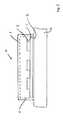
- Fig. 1 shows a schematic cross-sectional view through a first semiconductor module.
- a substrate for example a DCB substrate
- semiconducting components 2 for example power semiconductors, such as diodes, thyristors, IGBTs, MOSFETs or sensor components
- the semiconducting components 2 are partially surrounded by a housing 3.
- the housing 3 can - as in Fig. 1 shown - surround the substrate 1 rarium. But it can also be placed on the substrate 1.
- the reference numeral 4 denotes a potting compound, which the semiconducting components 2 and the substrate 1 at least partially covered and peripherally connected to a circumferential housing wall.
- the semiconductor module H thus constructed is mounted on a heat sink 6 with the interposition of a thermal compound 5.
- the potting compound 4 is formed here from a preceramic polymer, for example polysiloxane, which is filled to about 40 to 50 vol.% With a filler.
- the filler may be a SiC powder having a mean grain size, for example, in the range of 1 to 5 ⁇ m.
- the filler is embedded in the present in gel or thermoset preceramic polymer.
- the potting compound thus formed has an excellent thermal conductivity of more than 10 W / mK.
- a conventional housing 3 are first placed over the substrate 1, so that the substrate 1 rarium adjoins the peripheral housing wall. Subsequently, by a (not shown here) breakthrough in the housing 3, the potting compound 4 are filled. In this case, the preceramic polymer is present in a low-viscosity flowable form. In a next step, the potting compound 4 is then crosslinked, for example by increasing the temperature and placed in a gel-like or thermoset state. Thus, the housing 3 is firmly bonded to the substrate 1.
- the potting compound 4 forms an excellent thermal bridge of the semiconducting devices 2 to the housing 3 and from there into the environment. - A particularly good connection of the potting compound 4 to the housing 3 is achieved, although the housing 3 made of a present in thermosetting preceramic polymer is formed. In this case, the housing 3 has an excellent thermal conductivity ⁇ .
- Fig. 2 shows a schematic cross-sectional view through a second semiconductor module H.
- the in Fig. 1 shown housing 3 omitted.
- the potting compound 4 replaces the housing here. It is shaped in the manner of a housing and covers the semiconductive components 2, at least in sections, an upper side of the substrate 1 facing the semiconducting components 2, and advantageously a peripheral edge of the substrate 1.
- the production of a housing formed in a piece of potting compound 4 can be done for example by using a "lost shape".
- a set with the broken line housing form 7 can be placed on the substrate 1 or put over the substrate 1.
- the housing mold 7 is expediently made of the same material as the potting compound, wherein the preceramic polymer is present here in thermoset form.
- a provided in the housing mold 7 breakthrough (not shown here) poured the potting compound and then also transferred, for example, by a temperature increase in the thermoset state, so that the potting compound 4 and the housing mold 7 form a one-piece housing.
Landscapes
- Structures Or Materials For Encapsulating Or Coating Semiconductor Devices Or Solid State Devices (AREA)
- Cooling Or The Like Of Semiconductors Or Solid State Devices (AREA)
Applications Claiming Priority (1)
| Application Number | Priority Date | Filing Date | Title |
|---|---|---|---|
| DE102009000884A DE102009000884B3 (de) | 2009-02-16 | 2009-02-16 | Halbleitermodul mit Gehäuse aus präkeramischem Polymer |
Publications (2)
| Publication Number | Publication Date |
|---|---|
| EP2219217A2 true EP2219217A2 (fr) | 2010-08-18 |
| EP2219217A3 EP2219217A3 (fr) | 2010-11-03 |
Family
ID=42181545
Family Applications (1)
| Application Number | Title | Priority Date | Filing Date |
|---|---|---|---|
| EP20090016025 Withdrawn EP2219217A3 (fr) | 2009-02-16 | 2009-12-24 | Module semi-conducteur |
Country Status (3)
| Country | Link |
|---|---|
| EP (1) | EP2219217A3 (fr) |
| CN (1) | CN101807564A (fr) |
| DE (1) | DE102009000884B3 (fr) |
Families Citing this family (1)
| Publication number | Priority date | Publication date | Assignee | Title |
|---|---|---|---|---|
| DE102014211464A1 (de) * | 2014-06-16 | 2015-12-17 | Robert Bosch Gmbh | Halbleitermodul mit einer elektrisch isolierten Wärmesenke |
Citations (6)
| Publication number | Priority date | Publication date | Assignee | Title |
|---|---|---|---|---|
| EP0369652A2 (fr) * | 1988-11-12 | 1990-05-23 | Kureha Kagaku Kogyo Kabushiki Kaisha | Compositions de résine pour sceller un dispositif électronique et dispositifs électroniques scellés |
| US5436084A (en) | 1994-04-05 | 1995-07-25 | Dow Corning Corporation | Electronic coatings using filled borosilazanes |
| US5563102A (en) * | 1993-02-26 | 1996-10-08 | Dow Corning Corporation | Method of sealing integrated circuits |
| US6319740B1 (en) | 1995-10-27 | 2001-11-20 | Honeywell International Inc. | Multilayer protective coating for integrated circuits and multichip modules and method of applying same |
| EP1336990A1 (fr) * | 2002-02-14 | 2003-08-20 | Abb Research Ltd. | Boítier d' un module semi-conducteur de puissance résistant aux hautes tension |
| DE102004021927A1 (de) | 2004-05-04 | 2005-12-01 | Semikron Elektronik Gmbh & Co. Kg | Verfahren zur inneren elektrischen Isolation eines Substrats für ein Leistungshalbleitermodul |
Family Cites Families (3)
| Publication number | Priority date | Publication date | Assignee | Title |
|---|---|---|---|---|
| US5436083A (en) * | 1994-04-01 | 1995-07-25 | Dow Corning Corporation | Protective electronic coatings using filled polysilazanes |
| US5635240A (en) * | 1995-06-19 | 1997-06-03 | Dow Corning Corporation | Electronic coating materials using mixed polymers |
| JP2006206721A (ja) * | 2005-01-27 | 2006-08-10 | Kansai Electric Power Co Inc:The | 高耐熱合成高分子化合物及びこれで被覆した高耐電圧半導体装置 |
-
2009
- 2009-02-16 DE DE102009000884A patent/DE102009000884B3/de not_active Expired - Fee Related
- 2009-12-24 EP EP20090016025 patent/EP2219217A3/fr not_active Withdrawn
-
2010
- 2010-02-09 CN CN201010116688.1A patent/CN101807564A/zh active Pending
Patent Citations (6)
| Publication number | Priority date | Publication date | Assignee | Title |
|---|---|---|---|---|
| EP0369652A2 (fr) * | 1988-11-12 | 1990-05-23 | Kureha Kagaku Kogyo Kabushiki Kaisha | Compositions de résine pour sceller un dispositif électronique et dispositifs électroniques scellés |
| US5563102A (en) * | 1993-02-26 | 1996-10-08 | Dow Corning Corporation | Method of sealing integrated circuits |
| US5436084A (en) | 1994-04-05 | 1995-07-25 | Dow Corning Corporation | Electronic coatings using filled borosilazanes |
| US6319740B1 (en) | 1995-10-27 | 2001-11-20 | Honeywell International Inc. | Multilayer protective coating for integrated circuits and multichip modules and method of applying same |
| EP1336990A1 (fr) * | 2002-02-14 | 2003-08-20 | Abb Research Ltd. | Boítier d' un module semi-conducteur de puissance résistant aux hautes tension |
| DE102004021927A1 (de) | 2004-05-04 | 2005-12-01 | Semikron Elektronik Gmbh & Co. Kg | Verfahren zur inneren elektrischen Isolation eines Substrats für ein Leistungshalbleitermodul |
Also Published As
| Publication number | Publication date |
|---|---|
| DE102009000884B3 (de) | 2010-10-07 |
| CN101807564A (zh) | 2010-08-18 |
| EP2219217A3 (fr) | 2010-11-03 |
Similar Documents
| Publication | Publication Date | Title |
|---|---|---|
| EP3747048B1 (fr) | Composant électronique | |
| DE102013220880B4 (de) | Elektronisches Halbleitergehäuse mit einer elektrisch isolierenden, thermischen Schnittstellenstruktur auf einer Diskontinuität einer Verkapselungsstruktur sowie ein Herstellungsverfahren dafür und eine elektronische Anordung dies aufweisend | |
| DE102012224355B4 (de) | Leistungsmodul | |
| DE102014213564B4 (de) | Halbleitervorrichtung und Verfahren zu ihrer Herstellung | |
| DE102014104856B4 (de) | Explosionsgeschütztes Leistungshalbleitermodul | |
| DE112011103926T5 (de) | Halbleitervorrichtung und Verfahren zum Herstellen einer Halbleitervorrichtung | |
| DE102016117843A1 (de) | Mit Kühlfluid gekühlte und eine Abschirmschicht umfassende Packung | |
| DE102016107495A1 (de) | Vielschicht-Trägersystem, Verfahren zur Herstellung eines Vielschicht-Trägersystems und Verwendung eines Vielschicht-Trägersystems | |
| DE112014005694T5 (de) | Halbleitermodul | |
| DE102015115132B4 (de) | Halbleitermodul mit integrierter Stift- oder Rippenkühlstruktur und Verfahren zu seiner Herstellung | |
| DE102014100282A1 (de) | Chip-anordnung, verfahren zur herstellung einer chip-anordnung, integrierte schaltungen und verfahren zur herstellung einer integrierten schaltung | |
| DE102009044863A1 (de) | Halbleiter-Bauelement | |
| DE112018001769T5 (de) | Leistungsmodul und herstellungsverfahren des leistungsmoduls | |
| EP2219213B1 (fr) | Assemblage à semi-conducteurs | |
| DE102014213545A1 (de) | Leistungshalbleitermodul | |
| DE102015102041A1 (de) | Leistungsmodul | |
| DE102009000882A1 (de) | Substrat zur Aufnahme mindestens eines Bauelements und Verfahren zur Herstellung eines Substrats | |
| DE102009000884B3 (de) | Halbleitermodul mit Gehäuse aus präkeramischem Polymer | |
| DE102009000883B4 (de) | Substrat zur Aufnahme mindestens eines Bauelements und Verfahren zur Herstellung eines Substrats | |
| EP2278616B1 (fr) | Module semi-conducteur de puissance doté d'un sandwich équipé d'un composant semi-conducteur de puissance | |
| EP2219216B1 (fr) | Module semi-conducteur | |
| DE102019132314A1 (de) | Package mit Einkapselung unter Kompressionsbelastung | |
| WO2023094390A1 (fr) | Composant électronique et procédé de production | |
| DE102015223466A1 (de) | Elektrische Vorrichtung mit einer Umhüllmasse | |
| DE102007005234B4 (de) | Leistungselektronisches Modul mit einer Keramikumhüllung |
Legal Events
| Date | Code | Title | Description |
|---|---|---|---|
| PUAI | Public reference made under article 153(3) epc to a published international application that has entered the european phase |
Free format text: ORIGINAL CODE: 0009012 |
|
| AK | Designated contracting states |
Kind code of ref document: A2 Designated state(s): AT BE BG CH CY CZ DE DK EE ES FI FR GB GR HR HU IE IS IT LI LT LU LV MC MK MT NL NO PL PT RO SE SI SK SM TR |
|
| AX | Request for extension of the european patent |
Extension state: AL BA RS |
|
| PUAL | Search report despatched |
Free format text: ORIGINAL CODE: 0009013 |
|
| AK | Designated contracting states |
Kind code of ref document: A3 Designated state(s): AT BE BG CH CY CZ DE DK EE ES FI FR GB GR HR HU IE IS IT LI LT LU LV MC MK MT NL NO PL PT RO SE SI SK SM TR |
|
| AX | Request for extension of the european patent |
Extension state: AL BA RS |
|
| 17P | Request for examination filed |
Effective date: 20101014 |
|
| 17Q | First examination report despatched |
Effective date: 20110916 |
|
| STAA | Information on the status of an ep patent application or granted ep patent |
Free format text: STATUS: THE APPLICATION HAS BEEN WITHDRAWN |
|
| 18W | Application withdrawn |
Effective date: 20150821 |