EP2219334A2 - Mehrfachträgerübertragungsverfahren und -vorrichtung - Google Patents
Mehrfachträgerübertragungsverfahren und -vorrichtung Download PDFInfo
- Publication number
- EP2219334A2 EP2219334A2 EP20100164098 EP10164098A EP2219334A2 EP 2219334 A2 EP2219334 A2 EP 2219334A2 EP 20100164098 EP20100164098 EP 20100164098 EP 10164098 A EP10164098 A EP 10164098A EP 2219334 A2 EP2219334 A2 EP 2219334A2
- Authority
- EP
- European Patent Office
- Prior art keywords
- peak
- signal
- distortion
- baseband signals
- correction value
- Prior art date
- Legal status (The legal status is an assumption and is not a legal conclusion. Google has not performed a legal analysis and makes no representation as to the accuracy of the status listed.)
- Withdrawn
Links
- 230000003044 adaptive effect Effects 0.000 title claims abstract description 66
- 238000012545 processing Methods 0.000 claims abstract description 111
- 230000005540 biological transmission Effects 0.000 claims abstract description 79
- 238000012937 correction Methods 0.000 claims description 64
- 230000001629 suppression Effects 0.000 claims description 36
- 238000001914 filtration Methods 0.000 claims description 13
- 238000004891 communication Methods 0.000 claims description 12
- 239000000969 carrier Substances 0.000 claims description 7
- 230000000295 complement effect Effects 0.000 claims description 5
- 230000001186 cumulative effect Effects 0.000 claims description 5
- 230000003111 delayed effect Effects 0.000 claims description 5
- 238000005315 distribution function Methods 0.000 claims description 5
- 238000001514 detection method Methods 0.000 claims description 4
- 238000010295 mobile communication Methods 0.000 abstract description 13
- 238000000034 method Methods 0.000 description 27
- 238000010586 diagram Methods 0.000 description 13
- 238000001228 spectrum Methods 0.000 description 10
- 230000007423 decrease Effects 0.000 description 8
- 238000012544 monitoring process Methods 0.000 description 8
- 230000002123 temporal effect Effects 0.000 description 8
- 230000002542 deteriorative effect Effects 0.000 description 6
- 238000005070 sampling Methods 0.000 description 6
- 238000005259 measurement Methods 0.000 description 5
- 238000012360 testing method Methods 0.000 description 5
- 230000000694 effects Effects 0.000 description 4
- 101000647095 Homo sapiens Transcriptional protein SWT1 Proteins 0.000 description 3
- 108010076504 Protein Sorting Signals Proteins 0.000 description 3
- 102100025094 Transcriptional protein SWT1 Human genes 0.000 description 3
- 230000015572 biosynthetic process Effects 0.000 description 3
- 230000004044 response Effects 0.000 description 3
- 238000003786 synthesis reaction Methods 0.000 description 3
- 230000002194 synthesizing effect Effects 0.000 description 3
- 230000001131 transforming effect Effects 0.000 description 3
- 238000006243 chemical reaction Methods 0.000 description 2
- 238000007796 conventional method Methods 0.000 description 2
- 230000003247 decreasing effect Effects 0.000 description 2
- GRHWLIMQOFAGHA-UHFFFAOYSA-N dieticyclidine Chemical compound C=1C=CC=CC=1C1(N(CC)CC)CCCCC1 GRHWLIMQOFAGHA-UHFFFAOYSA-N 0.000 description 2
- 239000007937 lozenge Substances 0.000 description 2
- 238000004519 manufacturing process Methods 0.000 description 2
- 230000002411 adverse Effects 0.000 description 1
- 230000003321 amplification Effects 0.000 description 1
- 230000001413 cellular effect Effects 0.000 description 1
- 230000001934 delay Effects 0.000 description 1
- 238000009826 distribution Methods 0.000 description 1
- 230000007246 mechanism Effects 0.000 description 1
- 238000012986 modification Methods 0.000 description 1
- 230000004048 modification Effects 0.000 description 1
- 238000003199 nucleic acid amplification method Methods 0.000 description 1
- 230000009467 reduction Effects 0.000 description 1
- 239000004065 semiconductor Substances 0.000 description 1
- 238000004088 simulation Methods 0.000 description 1
- 238000010183 spectrum analysis Methods 0.000 description 1
- 230000007480 spreading Effects 0.000 description 1
- 238000003892 spreading Methods 0.000 description 1
Images


Classifications
-
- H—ELECTRICITY
- H04—ELECTRIC COMMUNICATION TECHNIQUE
- H04L—TRANSMISSION OF DIGITAL INFORMATION, e.g. TELEGRAPHIC COMMUNICATION
- H04L27/00—Modulated-carrier systems
- H04L27/26—Systems using multi-frequency codes
- H04L27/2601—Multicarrier modulation systems
- H04L27/2614—Peak power aspects
-
- H—ELECTRICITY
- H04—ELECTRIC COMMUNICATION TECHNIQUE
- H04L—TRANSMISSION OF DIGITAL INFORMATION, e.g. TELEGRAPHIC COMMUNICATION
- H04L27/00—Modulated-carrier systems
- H04L27/26—Systems using multi-frequency codes
- H04L27/2601—Multicarrier modulation systems
- H04L27/2614—Peak power aspects
- H04L27/2623—Reduction thereof by clipping
Definitions
- the present invention relates to a multicarrier transmission method and apparatus,and more particularly, to a method of suppressing a peak of a multicarrier transmitted signal, multicarrier transmission signal generating circuit with peak suppressing function, adaptive peak limiter, baseband signal processing LSI and multicarrier transmission apparatus.
- HSDPA High Speed Downlink Packet Access
- HSDPA is a technique where a plurality of users that perform downlink packet transmission shares a downlink channel, radio channel quality of each user is checked, and optimal base stations transmit signals to respective users, thus improving the transmission efficiency.
- Using the technique achieves a transmission rate of 10 Mbps using a frequency bandwidth of 5MHz.
- adaptive modulation that is a scheme for varying a modulation scheme and coding scheme corresponding to propagation environments and using M-ary modulation such as 16QAM and 64QAM suitable for large-capacity transmission
- M-ary modulation such as 16QAM and 64QAM suitable for large-capacity transmission
- HARQ Hybrid ARQ
- FCS Full Cell Selection
- a base station transmits signals with M-ary modulation such as 16QAM and 64QAM and high-rate coding with a coding rate of, for example, 3/4 when the reception quality in a mobile station is good, while transmitting signals with QPSK and low-rate coding with a coding rate of, for example, 1/4 when the reception quality in a mobile station is poor.
- M-ary modulation such as 16QAM and 64QAM
- high-rate coding with a coding rate of, for example, 3/4 when the reception quality in a mobile station is good
- QPSK and low-rate coding with a coding rate of, for example, 1/4 when the reception quality in a mobile station is poor.
- the CDMAsystem has a significant feature of implementing concurrent communications by multiplexing user signals.
- a frequency band assigned to a company permitted to locate base stations includes four channels (with carrier frequencies f1 to f4 respectively).
- data of a plurality of users is multiplexed on one channel, and signals of the channels are transmitted at the same time from a shared antenna.
- four carriers, f1 to f4 are concurrently transmitted (multicarrier transmission).
- a high-frequency amplifier provided at a last stage of a transmitter undergoes a heave load, and is required to secure the linearity in a wide band.
- the processing for suppressing an instantaneous peak is performed on a baseband signal for multicarrier transmission.
- the peak limiter is described in, for example, Japan Laid-Open Patent Publication Nos. 2002-164799 and 2002-44054 .
- HSDPA is an advanced technique with a considerable amount of difficulty to practically implement, in any theory.
- HSDPA needs to meet performance standard (TS25.141 Rel.5) stricter than performance standard (TS25.141 Rel.99) for general third-generation base station apparatus.
- the modulation scheme is varied corresponding to the channel quality.
- characteristics of a peak limiter are adapted to 64QAM with the strictest conditions as a reference and peak suppression is reduced, since the suppression on an instantaneous peak is not sufficient, and as a result, the load on a high-frequency amplifier in a subsequent stage is increased and the power efficiency in the high-frequency amplifier deteriorates. Meanwhile, when the peak suppression is enhanced, a signal loss degrades the signal quality.
- a method of suppressing a peak of a multicarrier transmission signal in a transmission system where filtering processing is performed on each of baseband signals respectively corresponding to a plurality of frequency channels using a filter, the signals subjected to the filtering processing are each multiplied by a predetermined carrier to be single-carrier signals, and the single-carrier signals are combined to obtain a multicarrier transmission signal, has the steps of branching each of the baseband signals from a regular signal processing route, performing filtering processing on each of the baseband signals branched, multiplying each of the baseband signals branched by the same carrier as the predetermined carrier at the same timing as in multiplication by the predetermined carrier, combining the signals obtained, and thereby obtaining a multicarrier signal for use in calculating a correction value for peak suppression, detecting an instantaneous peak of the multicarrier signal for use in calculating the correction value, and based on the detection result, obtaining the correction value for peak suppression, and multiplying each of the baseband signals
- a single-carrier signal is synthesized obtained by performing the same processing under the same condition as in the processing in the regular signal route, the same multicarrier signal as the regular multicarrier signal is obtained, a correction value is calculatedbased on the obtained signal, and using the correction value, an amplitude value of a baseband signal of each frequency channel is corrected.
- Such a method is equivalent to accurately predicting an instantaneous peak that will occur in synthesizing a single-carrier signal, and correcting the amplitude of a baseband signal in advance so as to keep the instantaneous peak within a desired level. In this way, it is possible to perform a method of suppressing a peak with extremely high reliability that has not been obtained before.
- the correction value is calculated using a high peak value obtained before the peak starts decreasing in a predetermined number of times, enabling severer peak limitation.
- a multicarrier transmission signal generating circuit with peak suppressing function has a regular signal processing route for branching each of baseband signals corresponding to each of frequency channels to multicarrier-transmit to two signal sequences, delaying each of baseband signals in one signal sequence in a delayer, multiplying each of the signals by a correction value for peak suppress in a multiplier, performing n-time (n is an integer of two or more) interpolation processing on each of the signals multiplied by the correction value, performing filtering processing on the signals using a filter, multiplying each of the signals by a carrier to obtain single-carrier signals, and combining the single-carrier signals to output a multicarrier transmission signal, and a correction value generating route for performing on each of baseband signals in the other signal sequence substantially the same processing at substantially the same timing as the n-time interpolation processing, the filtering processing, and processing of multiplying by the carrier to obtain a single-carrier signal in the regular signal processing route, thereby obtaining a multicarrier
- an instantaneous peak is detected based on a multicarrier signal synthesized through a route with the completely same conditions as in the regular multicarrier synthesis route to calculate the correction value for peak suppression, and it is thereby possible to perform extremely accurate peak suppressing correction.
- an adaptive peak limiter has a plurality of hard limiters which is provided respectively for a plurality of frequency channels having a possibility of containing communication data to which a predetermined data packet transmission scheme is applied, and limits an amplitude value of a baseb and signal of each of the frequency channels using an adaptive limit value provided from outside, and a limit value table to which access is made using, as an address variable, on/off bit information indicative of whether the predetermined data packet transmission scheme is applied and another on/off bit information indicative of whether each of the frequency channel is used, both the information being reported from an upper layer for each of the frequency channels, and which outputs an adaptive limit value as a result of the access to provide to at least one of the plurality of hard limiters.
- the adaptive peak limiter of the present invention is a new peak limiter contributing to implementation of, for example, High Speed Downlink Packet Access (HSDPA) supported by3.5-Generation Mobile Communications.
- HSDPA High Speed Downlink Packet Access
- the adaptive peak limiter of the present invention has a plurality of hard limiters which is provided respectively for frequency channels and whose limit values are updated adaptively.
- the "hard limiter” is a limiter with the capability of clamping a peak value of a signal in a predetermined value precisely.
- the adaptive peak limiter of the invention uses on/off information indicative of whether or not each frequency channel is used and another on/off information indicative of whether or not HSDPA is applied to chip data of each frequency channel notified from an upper layer (for example, a baseband processing board in a base station control section) on a chip basis of a baseband signal corresponding to each frequency channel in multicarrier transmission, the limit value table is accessed to output a limit value adaptively, and a clamp value of the hard limier is thereby adjusted finely on a chip basis.
- an upper layer for example, a baseband processing board in a base station control section
- concurrently transmitting signals of a plurality of frequency channels does not include using all the frequency channels always, and even when a chip of a transmission signal of a frequency channel is chip data using HSDPA (using QAM as a modulation scheme), chip data of the other frequency channels to concurrently transmit does not use HSDPA always (in other words, QPSK may be used as a modulation scheme).
- HSDPA using QAM as a modulation scheme
- the adaptive control is performed such that on a chip to which a modulation scheme with severe demodulation condition such as 16QAM is applied with frequency channel ON, the adaptive control with relieved suppression on amplitude value and importance placed on signal quality is performed, while when a frequency channel is OFF or on a chip to which HSDPA is not applied, adaptive control with enhanced suppression on limit value and importance placed on peak suppression is performed.
- a modulation scheme with severe demodulation condition such as 16QAM
- a baseband signal processing LSI has a configuration where respective signals of frequency channels output from the adaptive peak limiter as described above are input to the multicarrier transmission signal generating circuit with peak suppressing function as described above, thereby generating a multicarrier transmission signal subjected to peak suppressing processing such that a PAR (Peak to Average Ratio) value and a CCDF (Complementary Cumulative Distribution Function) remain within respective desired allowable ranges.
- PAR Peak to Average Ratio
- CCDF Complementary Cumulative Distribution Function
- the baseband signal processing LSI of the present invention uses the adaptive peak limiter of the invention and the multicarrier transmission signal generating circuit with peak suppressing function of the present invention in a combination thereof.
- peak limit processing is carried out in the multicarrier transmission signal generating circuit with peak suppressing function so that a PAR (Peak to Average Ratio) value and a CCDF (Complementary Cumulative Distribution Function) of a multicarrier signal always remain within respective desired allowable ranges (which assures that the total energy of the transmission signal always remains within a predetermined range), while using the peak limiter, a limit value is adaptively controlled for each frequency channel, and fine adjustment on distribution of transmission energy is carried out in response to a state of each frequency channel.
- PAR Peak to Average Ratio
- CCDF Complementary Cumulative Distribution Function
- the present invention it is possible to achieve latest mobile communications. For example, it is possible to achieve W-CDMA multicarrier transmission apparatuses in compliance with 3.5-Generation Mobile Communications supporting the HSDPA scheme.
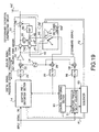
- FIGs.1A and 1B are block diagrams illustrating an entire configuration of a multicarrier transmission apparatus according to one embodiment of the present invention.
- the multicarrier transmission apparatus is a W-CDMA radio transmission apparatus (radio base station apparatus) that uses an adaptive peak limiter and multicarrier signal generating circuit each according to the present invention further in a combination with a hybrid distortion compensating circuit that performs distortion compensation with high precision.
- baseband signal processing section 600 is indicated by alternate long and short dashed lines.
- Adaptive peak limiter 400 and multicarrier signal generating circuit 500 with peak suppressing function are both indicated by dotted bold lines.
- hybrid distortion compensating circuit 700 has a configuration with a combination of adaptive pre-distortion section 14 and feedforward distortion compensating section 30. As other structural elements, the circuit 700 has D/A converter 20, A/D converter 28, switching circuit SW and high-frequency amplifier 32.
- transmission data d1 to d3 is multiplexed on frequency channel CH1
- transmission data d4 to d6, d7 to d9 and d10 to d12 is respectively multiplexed on frequency channels CH2 to CH4.
- Multiplexing sections 200a to 200d of user signal are provided respectively for frequency channels CH1 to CH4, and each has a plurality of spreading sections 2 and multiplexing circuit 4 that multiplexes spread user signals.
- Adaptive peak limiter 400 has hard limiters 300 provided for each frequency channel and limit value output circuit 350.
- Limit value output circuit 350 has address transforming circuit 352 and limit value table (ROM) 354.
- Address transforming circuit 352 transforms on/off information (F1 to F4) indicative of whether or not a respective frequency channel is used and another on/off information (DP1 to DP4) indicative of whether or not HSDPA is applied to chip data on the respective frequency channel notified on a chip basis from an upper layer (for example, a baseband processing board of a base station control section, not shown) to addresses for use in referring to ROM, and accesses to limit value table (ROM) 354 to cause adaptive limit value LIM to be output.
- F1 to F4 on/off information indicative of whether or not a respective frequency channel is used
- DP1 to DP4 another on/off information indicative of whether or not HSDPA is applied to chip data on the respective frequency channel notified on a chip basis from an upper layer (for example, a baseband processing board of a base station control section, not shown) to addresses for use in referring to ROM, and accesses to limit value table (ROM) 354 to cause adaptive limit value LIM to be output.
- Adaptive peak limiter 400 will be described specifically later with reference to FIGs.13 to 17 .
- Multicarrier signal generating circuit 500 with peak suppressing function performs n-time interpolation (n is an integer of two or more) and orthogonal modulation (by multiplying by respective one of orthogonal carriers el to e4 to obtain single-carrier signals) on four frequency channels, CH1 to CH4, and combines the single-carrier signals to generate a multicarrier transmission signal, while generating the same multicarrier signals as the above multicarrier signal in a route different from a regular signal processing route, calculating a correction value to correct an instantaneous peak based on the multicarrier signal, sending back the correction value to the regular signal processing route, and subjecting peak suppressing processing on a baseband signal to a baseband signal of each of the frequency channels.
- a baseband signal of each of frequency channels CH1 to CH4 is composed of two signals, I (in-phase) signal and Q (quadrature) signal, but for convenience in drawing, is indicated by a single signal line.
- frequency channel CH1 Since a configuration of circuitry for performing n-time interpolation and orthogonal modulation is the same as in each frequency channel, the description is given on frequency channel CH1.
- the circuitry for performing n-time interpolation and orthogonal modulation has a route for synthesizing a multicarrier signal to be a base to calculate a peak correction value, calculates the correction value based on the signal to provide to the regular signal processing route (indicated by bold lines in the figure), in addition to the regular signal processing route.
- the regular signal processing route (indicated by bold lines in the figure) has first delay circuit 508, multiplier 512 to multiply by a correction value, n-time interpolation circuit 514, low-pass filter (LPF) 516 to limit a band of a signal, multiplier 518 for orthogonal modulation, and combiner 590 that combines single-carrier signals passed through multiplier 518.
- First delay circuit 508 delays a signal by a time required for calculating the correction value and a time corresponding to a group delayof LPF 504.
- N-time interpolation circuit 514 performs interpolation for the need of increasing a clock frequency so as to perform signal processing for a predetermined wide frequency band.
- the orthogonal modulation is achieved by multiplying each of I and Q signals of each channel by the carrier el (to e4).
- a signal to transmit with the carrier frequency f1 is multiplied by a carrier of f1-fc, while multiplying a signal to transmit with the carrier frequency f2 by a carrier of f2-fc, to perform orthogonal modulation.
- the multiplication by the carrier el (to e4) is performed in the same way as in the signal processing route for calculating the correction value. Accordingly, in the circuit in FIGs.1A and 1B , a signal is multiplied by the carrier el (to e4) in the signal processing route for calculating the correction value, is delayed by a time required for calculating the correction value and a time corresponding to a group delay of low-pass filter (LPF) 516, and is subjected to orthogonal modulation in the regular signal processing route.
- LPF low-pass filter
- a signal route for synthesizing a multicarrier signal as a base for calculating the correction value is provided separately from the regular signal processing route.
- the signal processing route has n-time interpolation circuit 502, low-pass filter (LPF) 504, multiplier 506 and combiner 550.
- LPF low-pass filter
- a configuration of such a signal route and conditions such as signal processing timing in the route are completely the same as in the regular signal processing route.
- Correction value calculating section 570 that calculates a peak correction value based on the synthesized multicarrier signal has peak detecting section 572, relative comparison/determination section 574 and correction value calculating section 576.
- a peak suppressing control parameter is provided to relative comparison/determination section 574 from the outside, and it is thereby possible to adjust finely the peak suppressing capability depending on the relative level of importance between the signal quality and peak suppression.
- a peak limit value is provided to correction value calculating section 576 from the outside.
- a correction value output from correction value calculating section 576 is multiplied by a baseband signal in multiplier 512 in the regular signal processing route to correct the amplitude.
- the frequency band of a spectrum emission mask specified in 3GPP TS 25.104 is an extremely wide band that covers about 1 GHz between the upper and lower sides with a band of a transmission signal as a center. Since it is completely impossible for a general pre-distortion circuit to remove distortion components of the high orders occurring in such a wide band, using hybrid distortion compensating circuit 700 enables responses to such strict specifications.
- the multicarrier signal generating circuit with peak suppressing function, adaptive peak limiter and hybrid distortion compensating circuit will be described specifically below sequentially.
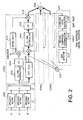
- FIG.2 is a block diagram illustrating a configuration of the multicarrier signal generating circuit with peak suppressing function.
- the multicarrier signal generating circuit has the same configuration as circuit 500 as shown in FIG. 1B .
- reference numerals 530a to 530d are circuits each for performing orthogonal modulation on a baseband signal subjected to amplitude correction to be a single-carrier signal.
- Correction value calculating circuit 570 calculates a correction value based on a multicarrier signal synthesized through completely the same processing as in the regular signal processing route.
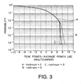
- FIG.3 is a graph of CCDF (Complementary Cumulative Distribution Function) indicative of the relationship between a ratio (horizontal axis) of peak power to average power of a multicarrier transmission signal generated in the multicarrier signal generating circuit with peak suppressing function in FIG.2 and probability (vertical axis).
- CCDF Complementary Cumulative Distribution Function
- characteristic line A is of peak suppressing control parameter (hold-num) of two.
- characteristic line B is of peak suppressing control parameter (hold-num) of zero
- characteristic line C is of peak suppressing control parameter (hold-num) of three.
- FIG.4 is a graph showing characteristics of each single-carrier signal prior to multicarrier synthesis in the multicarrier signal generating circuit with peak suppressing function in FIG.2 .
- FIG.7B is a graph showing characteristics of a signal subjected to peak suppression in the conventional circuit for suppressing a peak of a singe-carrier signal as shown in FIG.7A .
- FIG.4 it is understood that the circuit in FIG.2 does not perform extremely strict carrier suppression on a single-carrier signal.
- the multicarrier signal undergoes the peak limit to a high extent, and in any circumstances, the instantaneous peak of a multicarrier is assured to be kept within a predetermined range, while in terms of single-carrier signal, excessive peak limit is not performed, and accordingly, quality of the transmission signal is affected a little.
- a multicarrier signal is actually synthesized, an instantaneous peak of the signal is detected, and a correction value is calculated to suppress the instantaneous peak, whereby it is possible to suppress the instantaneous peak assuredly. Since thus peak limit with extremely high reliability is performed for multicarrier signal, it is possible to meet predetermined specifications even when strict conditions are imposed as in applying the HSDPA scheme.
- the present invention it is possible to finely adjust peak suppressing characteristics by setting the carrier suppressing control parameter (hold-num).
- FIG.6A illustrates a conventional peak limit circuit that performs limit processing on single-carrier signal S1
- FIG.6B shows characteristics of single-carrier signal S1.
- FIG.7A illustrates the same conventional peak limit circuit as in FIG.6A
- FIG.7B shows characteristics of the signal which has undergone peak suppression and is passed through low-pass filter (LPF) 203.
- LPF low-pass filter
- FIG.8A illustrates a conventional circuit that synthesizes a multicarrier signal using conventional peak limit circuits each shown in FIG. 6A arranged in parallel
- FIG.8B is a view showing characteristics of multicarrier signal S3 output from the circuit in FIG. 8A .
- peak detecting section 572 detects peak values of (M (n) to M(n+2)) of amplitude of baseband signals every 16 chips (herein, for convenience, baseband signals of 16 chips are assumed to be A(n) to A(n+2)).
- Relative comparison/determination section 574 and correction value calculating section 576 operate based on the flowchart shown in FIG.10 .
- step 802 When the determination result in step 802 is "yes”, in other words, the currently detected peak value is smaller than the temporal peak value and the number of times the value continuously decreases is 1, the peak suppressing control parameter (hold-iter) is incremented and updated (step 806), while, when the result is "no", that is, the currently detected peak value is larger than the temporal peak value, or decreases continuously two times, the currently detected peak value is set as a present value, and the peak suppressing control parameter (hold-iter) is initialized and returned to zero.
- correction value calculating section 576 compares the limit value (limit-value) with the temporal peak value (step 808), and when the temporal peak value is larger, calculates a correction value for peak suppression using the temporal peak value (step 810), while, when the temporal peak value is smaller, making a correction value "1" because the peak suppression is not required (step 812).
- the correction value is multiplied by the baseband signal (step 814), and the processing flow proceeds to a next step (step 816).
- FIG.11 illustrates a specific example of calculating a correction value.
- the peak value increases during a period of from time t(n-1) to t(n+1), then decreases continuously, and decreases below the limit value (limit-value) at time t(n+5).
- processing as shown in the figure is executed at each time. It is noted that at time t(t+2) and t (n+3), even the peak value decreases, the correction value based on a large peak value immediately before the peak value starts decreasing, that is, correction value (n+1) is used, and thus adaptive control is performed with importance placed on peak suppression.
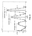
- FIG.12 shows changes in the degree of amplitude suppression of baseband signal when the set value (hold-num) of peak suppressing control parameter is "0" or "2".
- the set value (hold-num) of peak suppressing control parameter of "2" has a larger effect of peak suppression.
- the adaptive peak limiter will be described below with reference to FIGs.13 to 17 .
- FIG.13 is a block diagram illustrating a configuration of the adaptive peak limiter.
- limit value output section 350 refers to the limit value table (lookup table) 354 to cause the limit value LIM to be output.
- the hard limiter 300 has amplitude calculating section 310 that calculates amplitude Xn of each of input I and Q signals, comparing section 320 that compares the calculated amplitude with the limit value LIM, correction value calculating section 330 that calculates a correction value from the input I and Q signals, amplitude Xn and limit value LIM, and switch circuits SWT1 and SWT2.
- switches SWT1 and SWT2 are each switched, and when amplitude of an input signal exceeds the limit value LIM, the switches are switched to respective "a" terminals, while being switched to respective "b” terminals when amplitude of an input signal is less than the limit value LIM.
- switches SWT1 and SWT2 are switched to respective "b" terminals, the input signal is not corrected and output.
- FIG.14A is a view showing characteristics of an output signal of the hard limiter when the limit value is P0, P1 or P2, and FIG.14B is a view showing the relative relationship between the limit value and quality of a transmission signal.
- FIG.15 is a timing diagram illustrating states of baseband signals of four frequency channels CH1 to CH4 (each channel has two signals sequences, I and Q, and thus there are eight inputs) associated with sates of the on/off information (F1 to F4) indicative of whether or not a respective frequency channel is used and another on/off information (DP1 to DP4) indicative of whether or not HSDPA is applied to chip data on the respective frequency channel notified on a chip basis from baseband control board 910 in base station (BTS) control section 900.
- BTS base station
- FIG.15 does not show data of frequency channels CH2 and CH3.
- shaded chips are chips to which HSDPA is applied.
- the HSDPA application on/off information (DP1 to DP4) is high level on chips to which HSDPA is applied, and similarly, frequency on/off information (F1 to F4) is high level when a frequency channel is used.
- the HSDPA application on/off information (DP1 to DP4) and frequency on/off information (F1 to F4) is collectively transformed into address information of eight bits.
- “on” of each piece of information corresponds to "1”
- “off” corresponds to "0”.
- ROM address is associated with ROM data (data of limit value), andROMdata (data of limit value) is written in ROM to generate a lookup table.
- situations 1 to 7 are assumed.
- the limit value is set such that a greater limit value is applied to a frequency channel that uses HSDPA than a frequency channel that does not use HSDPA to prevent signal quality from deteriorating, and that in a case where an unused frequency channel is present, as the number of unused frequency channels is increased, the limit value for use in a used frequency channel is increased, to prevent signal quality from deteriorating.
- L2 is greater than L1.
- L3 is calculated by obtaining a fraction of a denominator that is the number of frequency channels with frequency on/off bit on and a numerator of 4, raising the fraction to the power of 1/2, and further multiplying the resultant by L1.
- L4 is calculated by obtaining a fraction of a denominator that is the number of frequency channels with frequency on/off bit on and a numerator of 4, raising the fraction to the power of 1/2, and further multiplying the resultant by L2.
- FIGs.17A and 17B are views each showing an example of effects in the case of applying the adaptive peak limiter.
- FIG.17A is a view showing results of measurements (simulation) of error vector magnitude that is an index to evaluate the signal quality on samples (plotted by white circles) to which HSDPA is not applied and samples (plotted by lozenges with black-shaded half) to which DSDPA is applied.
- standard A is a requirement (criterion by which to evaluate samples plotted by white circles) in 3GPP R99
- standard B is a requirement (criterion by which to evaluate samples plotted by lozenges with black-shaded half) in 3GPP R5.
- FIG.17B shows samples measured on peak code domain error, where standard C is a requirement in 3GPP R99, and standard D is a requirement in 3GPP R5.
- FIGs.18A and 18B are graphs each showing an example of a result of measuring the degree of peak suppression of a multicarrier transmission signal output from the baseband signal processing LSI as illustrated in FIG.1 , using test model 1 or test model 3 of 3GPP.
- the present invention it is possible to suppress instantaneous peaks of the entire multicarrier transmission signal to be within a desired range in any cases, while finely adjusting the amplitude of the transmission signal depending on situation of each frequency channel, and to achieve both peak suppression and assurance of signal quality.
- the hybrid distortion compensating circuit (including a high-frequency amplifier) shown in FIG.19 (and in FIG.1B ) will be described specifically.
- CDMA multicarrier communications require higher linearity in a high-frequency power amplifier than in other mobile communications. Therefore, power efficiency deteriorates remarkably unless the linearity of a power amplifier is compensated using distortion compensating techniques such as adaptive pre-distortion.
- An input signal of a power amplifier has, for example, a bandwidth of 15 MHz to 20 MHz. Accordingly, the band of a distortion ranges from about 100 MHz to 200 MHz.
- the adaptive pre-distortion processing since it is necessary for an output signal of the power amplifier to be returned to the digital signal processing system, it is similarly required to perform A/D conversion with a sampling frequency of from about 100 MHz to 200 MHz the same as the band of the distortion component.
- D/A converters and A/D converters require the resolution of from 12 bits to 16 bits.
- the hybrid distortion compensating circuit in FIG.19 limits a band of a signal (input baseband signal) to which the adaptive pre-distortion processing is applied to frequencies enabling the resolution of 12 bits to 16 bits in the D/A converter and A/D converter.
- the feedforward distortion compensating circuit with characteristics accurately adjusted effectively removes distortion (distortion of high order) occurring in a band of higher frequencies by digital signal processing.
- the hybrid distortion compensatingcircuit has, asprimary structural elements, adaptive pre-distortion section (digital signal processing section) 14, high-frequency power amplifier 32, feedforward distortion compensating circuit (high-frequency power analog circuit) 30 with two input terminals TA1 and TA2, high-frequency switching circuit (hereinafter, simply referred to as a switching circuit) SW to fetch selectively either of two input signals, output signal and feedforward loop signal of feedforward' distortion compensating circuit 30, control/monitoring section (belonging to the digital signal processing system), amplitude/phase/delay adjustor 51 that adjusts the amplitude (gain), phase and delay of a standard signal (that is an input signal (IN) of the distortion compensating circuit) provided to input terminal TA2 of feedforward distortion compensating circuit 30, and sequencer 80 that controls switching of switching circuit SW and provides information (P1 and P2) required for causing sections to operate sequentially to the sections.
- a switching circuit to fetch selectively either of two input signals, output signal and feedforward loop signal of feedforward' distortion compensating circuit 30,
- a signal path on which signals are provided and received between the digital signal processing system and analog signal processing system is provided with D/A converters 20 and 56, A/D converter 28 and frequency converting circuit.
- the frequency converting circuit has RF carrier oscillator 24, and mixers 22, 26 and 58 as structural elements.
- feedforward distortion compensating circuit 30 has input terminal TA1 to input a signal including a distortion component (linear distortion component remaining without being removed by pre-distortion distortion compensation) to a main path, and input terminal TA2 to input a standard signal that does not include distortion to the feedforward loop.
- the main path is a line connecting input terminal TA1 and combiner 38.
- the feedforward loop has attenuator 42 that adjusts signal amplitude, combiner 46 to separate a distortion component from a signal of the main path, error amplifier 48 that amplifies the amplitude of a signal of a distortion component, shifter 50 to invert a phase of an output signal of error amplifier 46, and combiner 38 to return an output signal of shifter 50 to the main path.
- the hybrid distortion compensating circuit has a hybrid structure with a combination of adaptive pre-distortion section 14 that performs adaptive pre-distortion processing on baseband digital signals and feedforward distortion compensating circuit 30.
- feedforward distortion compensation executes distortion compensation in the order in which signals are input and output, while adaptive pre-distortion distortion compensation is feedback type of distortion compensation, thus signal routes are different therebetween, and therefore, in order to combine both the schemes, it is required to divide both schemes into respective unit elements to facilitate combining both schemes, and configure again a hybrid structure.
- feedforward distortion compensating circuit 30 is provided with two input terminals TA1 and TA2, and thus provided with a new configuration to receive as its inputs independently of each other an output signal (including a remaining distortion component that cannot be removed by pre-distortion distortion compensation) of high-frequency power amplifier 32, and a standard signal that does not include distortion, thereby enabling a combination of different types of distortion compensating circuits.
- the distortion compensating processing in the hybrid distortion compensation method is principally divided into two kinds of processing.
- the adaptive pre-distortion distortion compensation in full-digital control removes with high stability a distortion component of low order of the high-frequency power amplifier that is a distortion component with a high level within sampling frequency band of D/A converters 20 and 56 and A/D converter 28.
- the distortion cancellation with high precision in feedforward distortion compensating circuit 30 is achieved on the assumption that two signals respectively input to two input terminals TA1 and TA2 are in completely agreement with each other in input level (amplitude), phase and delay.
- the distortion compensating circuit (hybrid distortion compensating circuit) in FIG.19 is provided with an adjustment mechanism that performs adjustments so as to bring each of amplitude and others of two signals input to feedforward distortion compensating circuit 30 into completely coincident with respective one another, and in this respect, the distortion compensating circuit of the present invention has an extremely important feature.
- control/monitoring section 60 measures precisely differences (at least a difference in either of characteristics) in amplitude (gain), initial phase and transmission delay between two input signals of feedforward distortion compensating circuit 30.
- the adjustor 50 for amplitude and others adjusts at least one of the amplitude, phase and delay of a standard signal (input signal (IN) of the distortion compensating circuit) so as to cancel the measured difference.
- a standard signal input signal (IN) of the distortion compensating circuit
- a distortion component with a high level is not input to error amplifier 48 existing in the feedforward loop. It is thereby possible to set the error amplifier for a low power amplification rate, thus contributing to reduced power consumption.
- switching circuit SW After finishing the pre-distortion processing and characteristic adjustments of two signals of feedforward distortion compensating circuit 30, switching circuit SW outputs an output signal (signal A4 in FIG.19 ) of feedforward distortion compensating circuit 30 to return to the digital signal processing system.
- Control/monitoring section 60 monitors the characteristics of feedback signals, and when desired precision cannot be assured in distortion compensation, executes again sequentially the pre-distortion processing and characteristic adjustments of two signals of feedforward distortion compensating circuit 30.
- the order of signal processing is controlled by sequencer 80.
- the switching circuit (SW) is switched to "d" terminal side, and adaptive pre-distortion processing is carried out (state 1, step 100).
- the switching circuit (SW) is next switched to "a" terminal side.
- the switching circuit (SW) is next switched to "b" terminal side, thus shifting to state 3 to check a result of adjustment in state 2.
- a power level (leak level of the standard signal) of components of the standard signal is measured except a distortion signal in the feedforward loop (step 104). It is determined whether or not the leak-level exceeds a threshold, that is, whether the leak amount is allowable (OK) or not, and at the time of NG, the processing flow returns to step 102, while proceeding to state 4 at the time of OK (step 106).
- the switching circuit (SW) is switched to "c" terminal side. Then, the frequency spectrum of a final output signal of the distortion compensating circuit is measured, and compared with a predetermined standard mask pattern (spectrum emission mask pattern) to determine a state of suppression in distortion on the frequency axis (step 108).
- a predetermined standard mask pattern spectrum emission mask pattern
- step 110 when the frequency spectrum is suppressed to be within an allowable range (step 110), the processing flow returns to step 108 to continue monitoring, while returning to step 100 when the spectrum is not suppressed (step 110) to execute the above-mentioned processing sequentially.
- FIGs.21A to 21D respectively show frequency spectra of the input signal (the number of carrier is "3"), pre-distortion signal, standard signal in the feedforward distortion compensation and output signal in the circuit in FIG.19 .
- the hybrid distortion compensating circuit in FIG.19 has adaptive pre-distortion section 14 that provides an input digital signal with distortion with inverse characteristics to non-linear characteristics of the power amplifier, and feedforward distortion compensating circuit 30 that compensates for a distortion component, which cannot be compensated in adaptive pre-distortion section 14, by feedforward loop, where feedforward distortion compensating circuit 30 has two signal input terminals TA1 and TA2 enabling two signals to be input separately, a signal subjected to the adaptive pre-distortion processing in pre-distortion section 14 is input to one bf the signal input terminals, TA1, while a standard signal is input to the other one of the signal input terminals, TA2, and the standard signal corresponds to an input digital signal prior to the pre-distortion processing in pre-distortion section 14, and thus connects both circuits in a manner capable of drawing maximum characteristics of each circuit.
- the distortion compensating circuit in FIG.19 is a new distortion compensating circuit in full-digital control having a circuit structure connecting a digital signal processing circuit and high-frequency power analog circuit via a signal path containing D/A converters and A/D converter.
- the distortion compensating circuit preferably performs processing of following items 1 to 5 and obtains effectiveness as described below.
- the distortion compensation with high accuracy is carried out in the hybrid distortion compensating circuit, it is possible to assure the quality with a desired level in transmission signal.
- the present invention is applicable to other communication systems.
- the peak limiter of the present invention is applicable to other CDMA communication systems that support high speed packet transmission.
Landscapes
- Engineering & Computer Science (AREA)
- Computer Networks & Wireless Communication (AREA)
- Signal Processing (AREA)
- Transmitters (AREA)
- Digital Transmission Methods That Use Modulated Carrier Waves (AREA)
- Mobile Radio Communication Systems (AREA)
Applications Claiming Priority (2)
| Application Number | Priority Date | Filing Date | Title |
|---|---|---|---|
| JP2002224221A JP3796204B2 (ja) | 2002-07-31 | 2002-07-31 | マルチキャリア送信信号のピーク抑圧方法およびピーク抑圧機能をもつマルチキャリア送信信号生成回路 |
| EP20030016801 EP1387541B1 (de) | 2002-07-31 | 2003-07-23 | Verringerung des Verhältnisses von Spitzen- zu Durchschnittsleistung |
Related Parent Applications (1)
| Application Number | Title | Priority Date | Filing Date |
|---|---|---|---|
| EP03016801.7 Division | 2003-07-23 |
Publications (2)
| Publication Number | Publication Date |
|---|---|
| EP2219334A2 true EP2219334A2 (de) | 2010-08-18 |
| EP2219334A3 EP2219334A3 (de) | 2013-01-23 |
Family
ID=30112976
Family Applications (2)
| Application Number | Title | Priority Date | Filing Date |
|---|---|---|---|
| EP20030016801 Expired - Lifetime EP1387541B1 (de) | 2002-07-31 | 2003-07-23 | Verringerung des Verhältnisses von Spitzen- zu Durchschnittsleistung |
| EP20100164098 Withdrawn EP2219334A3 (de) | 2002-07-31 | 2003-07-23 | Adaptiver Spitzenwertbegrenzer in einem Mehrträgersystem |
Family Applications Before (1)
| Application Number | Title | Priority Date | Filing Date |
|---|---|---|---|
| EP20030016801 Expired - Lifetime EP1387541B1 (de) | 2002-07-31 | 2003-07-23 | Verringerung des Verhältnisses von Spitzen- zu Durchschnittsleistung |
Country Status (5)
| Country | Link |
|---|---|
| US (2) | US6982965B2 (de) |
| EP (2) | EP1387541B1 (de) |
| JP (1) | JP3796204B2 (de) |
| CN (2) | CN101056299B (de) |
| DE (1) | DE60332798D1 (de) |
Families Citing this family (35)
| Publication number | Priority date | Publication date | Assignee | Title |
|---|---|---|---|---|
| JP4287225B2 (ja) * | 2003-09-18 | 2009-07-01 | 株式会社日立国際電気 | 送信機 |
| GB2406300A (en) * | 2003-09-20 | 2005-03-30 | Rolls Royce Plc | A method of laser machining components having a protective surface coating |
| JP2005101975A (ja) * | 2003-09-25 | 2005-04-14 | Matsushita Electric Ind Co Ltd | 無線通信装置及びピーク抑圧方法 |
| JP2005106684A (ja) * | 2003-09-30 | 2005-04-21 | Konica Minolta Medical & Graphic Inc | 放射線画像変換パネル及びその製造方法 |
| US7342976B2 (en) * | 2004-01-27 | 2008-03-11 | Crestcom, Inc. | Predistortion circuit and method for compensating A/D and other distortion in a digital RF communications transmitter |
| JP2005252509A (ja) * | 2004-03-03 | 2005-09-15 | Nec Corp | マルチキャリア伝送用非線形歪補償回路 |
| JP4359191B2 (ja) * | 2004-06-01 | 2009-11-04 | 株式会社日立国際電気 | 信号生成装置 |
| DE102004038089B4 (de) * | 2004-08-05 | 2016-02-04 | Rohde & Schwarz Gmbh & Co. Kg | Reglergestütztes Verfahren und reglergestützte Vorrichtung zur Bestimmung der Kennlinie eines Kompensationsgliedes in einem Pegelkreis |
| JP2006174364A (ja) * | 2004-12-20 | 2006-06-29 | Fujitsu Ltd | マルチキャリア信号送信装置、マルチキャリア信号受信装置、マルチキャリア信号送信方法、マルチキャリア信号受信方法、及び通信システム |
| GB0500415D0 (en) * | 2005-01-10 | 2005-02-16 | Nokia Corp | Transmitting information using multiple carriers |
| GB0500416D0 (en) * | 2005-01-10 | 2005-02-16 | Nokia Corp | Transmitting information using multiple carriers |
| CN101133674B (zh) * | 2005-03-02 | 2011-08-03 | 日本电气株式会社 | 下行链路分组通信的传输控制方法和无线基站 |
| KR101256155B1 (ko) * | 2005-08-19 | 2013-04-19 | 지티이 코포레이션 | 시분할-동기식 코드 분할 다중 접속 시스템의 다중 캐리어고속 하향 패킷 접속 구현 방법 |
| US20070071120A1 (en) * | 2005-09-26 | 2007-03-29 | Shilpa Talwar | Peak to average power reduction using channel state information |
| EP1940058B1 (de) * | 2005-09-27 | 2013-11-13 | Fujitsu Ltd. | Funkübertragungseinrichtung mit spitzenunterdrückungsfunktion |
| KR100707268B1 (ko) * | 2005-10-08 | 2007-04-16 | 삼성전자주식회사 | 영상보간장치 및 영상보간방법 |
| KR101150611B1 (ko) * | 2005-10-21 | 2012-06-08 | 삼성전자주식회사 | 이동통신 시스템에서 복합 자동 재전송 방식을 이용한 패킷데이터 송/수신 장치 및 방법 |
| JP2007194825A (ja) * | 2006-01-18 | 2007-08-02 | Fujitsu Ltd | マルチキャリア信号送信装置 |
| EP1821474B1 (de) | 2006-02-17 | 2012-05-30 | Fujitsu Limited | Einrichtung zum Entfernen von Spitzenspannungsignalen |
| JP4789749B2 (ja) * | 2006-08-17 | 2011-10-12 | 富士通株式会社 | ピーク抑圧装置 |
| JP4847838B2 (ja) * | 2006-10-13 | 2011-12-28 | 株式会社日立国際電気 | 送信機 |
| US8306162B2 (en) * | 2007-11-28 | 2012-11-06 | Motorola Solutions, Inc. | Method and apparatus for complementary cumulative distribution driven level convergence for spectrum sensing |
| JP4941261B2 (ja) | 2007-12-04 | 2012-05-30 | 富士通株式会社 | 歪補償増幅装置および歪補償方法 |
| JP5176692B2 (ja) | 2008-05-28 | 2013-04-03 | 日本電気株式会社 | 歪補償回路及び歪補償方法 |
| JP5125797B2 (ja) * | 2008-06-19 | 2013-01-23 | 富士通株式会社 | 振幅抑圧装置および信号送信装置 |
| JP5233784B2 (ja) * | 2009-03-25 | 2013-07-10 | 日本電気株式会社 | マルチキャリア送信信号のピークファクタ低減装置及び方法 |
| JP2011176790A (ja) * | 2010-01-26 | 2011-09-08 | Kyocera Corp | 通信装置および通信方法 |
| JP5406132B2 (ja) * | 2010-07-08 | 2014-02-05 | 株式会社日立製作所 | ピークファクタ低減装置および無線送信機 |
| EP2761739B1 (de) * | 2011-09-30 | 2019-08-07 | Aviat Networks, Inc. | Systeme und verfahren für adaptive stromverstärkerlinearisierung |
| US8995521B2 (en) | 2012-10-30 | 2015-03-31 | Lsi Corporation | Method and apparatus for high density pulse density modulation |
| US9086556B2 (en) * | 2013-02-12 | 2015-07-21 | Nexans | Fiber optic cable with improved flexibility, low temperature and compression resistance |
| JP6175852B2 (ja) * | 2013-03-28 | 2017-08-09 | 富士通株式会社 | 電力増幅装置 |
| KR102200813B1 (ko) * | 2014-11-19 | 2021-01-11 | 삼성전자 주식회사 | 이동 통신 시스템에서 신호 수신 방법 및 장치 |
| US9590567B2 (en) * | 2015-07-02 | 2017-03-07 | Xilinx, Inc. | Moving mean and magnitude dual path digital predistortion |
| US11838121B2 (en) * | 2021-07-01 | 2023-12-05 | Qualcomm Incorporated | Downlink transmission requirement based on downlink compensation capability of a user equipment |
Citations (2)
| Publication number | Priority date | Publication date | Assignee | Title |
|---|---|---|---|---|
| JP2002044054A (ja) | 2000-07-25 | 2002-02-08 | Hitachi Kokusai Electric Inc | リミッタ回路付きキャリア合成送信回路 |
| JP2002164799A (ja) | 2000-11-24 | 2002-06-07 | Matsushita Electric Ind Co Ltd | 送信電力制御方法及びその装置並びに通信装置 |
Family Cites Families (38)
| Publication number | Priority date | Publication date | Assignee | Title |
|---|---|---|---|---|
| US12292A (en) * | 1855-01-23 | Henry biakely | ||
| US86507A (en) * | 1869-02-02 | Improvement in whip-sockets | ||
| US61068A (en) * | 1867-01-08 | Improved apparatus for forming boilers | ||
| US101935A (en) * | 1870-04-12 | Improvement in treating fatty matters for the manufacture of candles | ||
| US12403A (en) * | 1855-02-20 | Frederick denzler | ||
| US118729A (en) * | 1871-09-05 | Improvement in carriage-shackles | ||
| US63685A (en) * | 1867-04-09 | Andrew r | ||
| US6157A (en) * | 1849-03-10 | Delivery amd take-tip motion of looms | ||
| US101936A (en) * | 1870-04-12 | Improvement in churns | ||
| US5357541A (en) | 1989-03-23 | 1994-10-18 | Echelon Corporation | Transceiver providing selectable frequencies and spreading sequences |
| US5125100A (en) | 1990-07-02 | 1992-06-23 | Katznelson Ron D | Optimal signal synthesis for distortion cancelling multicarrier systems |
| US5093840A (en) | 1990-11-16 | 1992-03-03 | Scs Mobilecom, Inc. | Adaptive power control for a spread spectrum transmitter |
| US5107225A (en) | 1990-11-30 | 1992-04-21 | Qualcomm Incorporated | High dynamic range closed loop automatic gain control circuit |
| US6334219B1 (en) * | 1994-09-26 | 2001-12-25 | Adc Telecommunications Inc. | Channel selection for a hybrid fiber coax network |
| CN1075301C (zh) | 1994-12-05 | 2001-11-21 | Ntt移动通信网株式会社 | 信号多路复用器及多路复用方法 |
| JPH08274734A (ja) | 1994-12-05 | 1996-10-18 | N T T Ido Tsushinmo Kk | 信号多重化装置及び方法 |
| GB2296165B (en) * | 1994-12-15 | 1999-12-29 | Int Mobile Satellite Org | Multiplex communication |
| EP0735731B1 (de) * | 1995-03-31 | 2004-05-12 | Victor Company Of Japan, Limited | Mehrträgenmodulator- und -demodulator mit Einrichtungen zur Verringerung der Spitzenleistung |
| ZA965340B (en) | 1995-06-30 | 1997-01-27 | Interdigital Tech Corp | Code division multiple access (cdma) communication system |
| JP2718398B2 (ja) | 1995-06-30 | 1998-02-25 | 日本電気株式会社 | Cdma基地局送信装置 |
| GB2309363B (en) | 1996-01-17 | 2000-07-12 | Motorola Ltd | Multicarrier communication system and method for peak power control |
| JP3462388B2 (ja) * | 1998-04-28 | 2003-11-05 | 松下電器産業株式会社 | 無線通信装置 |
| US6590906B1 (en) * | 1998-08-24 | 2003-07-08 | Matsushita Electric Industrial Co., Ltd. | Multi-carrier transmitter circuit and communication equipment |
| US6188732B1 (en) | 1998-10-19 | 2001-02-13 | Samsung Electronics Co., Ltd. | Digital feedforward amplifier for use in an RF transmitter and method of operation |
| GB9823145D0 (en) * | 1998-10-23 | 1998-12-16 | Philips Electronics Nv | Radio communication system |
| US6236864B1 (en) | 1998-11-27 | 2001-05-22 | Nortel Networks Limited | CDMA transmit peak power reduction |
| US6931053B2 (en) * | 1998-11-27 | 2005-08-16 | Nortel Networks Limited | Peak power and envelope magnitude regulators and CDMA transmitters featuring such regulators |
| US6430213B1 (en) | 1999-05-26 | 2002-08-06 | The Aerospace Corporation | Coherent adaptive subcarrier modulation method |
| US6654427B1 (en) * | 1999-07-28 | 2003-11-25 | Lucent Technologies Inc. | Signal notching system for limiting signal peaks |
| WO2001065748A1 (fr) | 2000-02-29 | 2001-09-07 | Fujitsu Limited | Procede de codage pour transmission a porteuses multiples et codeur utilisant ce procede |
| JP4313925B2 (ja) | 2000-03-17 | 2009-08-12 | 富士通株式会社 | マルチキャリア直接拡散送受信システム,マルチキャリア直接拡散送受信機,マルチキャリア直接拡散送信機及びマルチキャリア直接拡散受信機 |
| US6449302B2 (en) | 2000-04-19 | 2002-09-10 | Powerwave Technologies, Inc. | System and method for peak power reduction in spread spectrum communications systems |
| US7061990B2 (en) | 2000-07-21 | 2006-06-13 | Pmc-Sierra Inc. | Systems and methods for the dynamic range compression of multi-bearer single-carrier and multi-carrier waveforms |
| IT1318964B1 (it) | 2000-10-04 | 2003-09-19 | Cit Alcatel | Metodo per ridurre il rapporto tra potenza di picco e potenza media diun segnale multiportante generato da traformata di fourier in sistemi |
| US7170952B2 (en) | 2001-07-02 | 2007-01-30 | Powerwave Technologies, Inc. | System and method for post filtering peak power reduction in communications systems |
| US6931239B2 (en) * | 2001-07-30 | 2005-08-16 | Hitachi Kokusai Electric Inc. | Peak limiter and multi-carrier amplification apparatus |
| US7095798B2 (en) * | 2001-08-02 | 2006-08-22 | Powerwave Technologies, Inc. | System and method for post filtering peak power reduction in multi-carrier communications systems |
| US20030086507A1 (en) | 2001-11-07 | 2003-05-08 | Jaehyeong Kim | Peak limiting architecture and method |
-
2002
- 2002-07-31 JP JP2002224221A patent/JP3796204B2/ja not_active Expired - Lifetime
-
2003
- 2003-07-22 US US10/623,811 patent/US6982965B2/en not_active Expired - Lifetime
- 2003-07-23 EP EP20030016801 patent/EP1387541B1/de not_active Expired - Lifetime
- 2003-07-23 EP EP20100164098 patent/EP2219334A3/de not_active Withdrawn
- 2003-07-23 DE DE60332798T patent/DE60332798D1/de not_active Expired - Lifetime
- 2003-07-31 CN CN2007101028729A patent/CN101056299B/zh not_active Expired - Fee Related
- 2003-07-31 CN CNB031327893A patent/CN100345401C/zh not_active Expired - Fee Related
-
2005
- 2005-06-30 US US11/169,705 patent/US7460500B2/en not_active Expired - Fee Related
Patent Citations (2)
| Publication number | Priority date | Publication date | Assignee | Title |
|---|---|---|---|---|
| JP2002044054A (ja) | 2000-07-25 | 2002-02-08 | Hitachi Kokusai Electric Inc | リミッタ回路付きキャリア合成送信回路 |
| JP2002164799A (ja) | 2000-11-24 | 2002-06-07 | Matsushita Electric Ind Co Ltd | 送信電力制御方法及びその装置並びに通信装置 |
Also Published As
| Publication number | Publication date |
|---|---|
| US6982965B2 (en) | 2006-01-03 |
| JP3796204B2 (ja) | 2006-07-12 |
| EP1387541B1 (de) | 2010-06-02 |
| JP2004064711A (ja) | 2004-02-26 |
| US7460500B2 (en) | 2008-12-02 |
| CN101056299B (zh) | 2012-05-09 |
| CN1496037A (zh) | 2004-05-12 |
| CN100345401C (zh) | 2007-10-24 |
| CN101056299A (zh) | 2007-10-17 |
| EP1387541A3 (de) | 2007-02-14 |
| US20040136395A1 (en) | 2004-07-15 |
| US20050243909A1 (en) | 2005-11-03 |
| EP2219334A3 (de) | 2013-01-23 |
| DE60332798D1 (de) | 2010-07-15 |
| EP1387541A2 (de) | 2004-02-04 |
Similar Documents
| Publication | Publication Date | Title |
|---|---|---|
| EP1387541B1 (de) | Verringerung des Verhältnisses von Spitzen- zu Durchschnittsleistung | |
| US8982995B1 (en) | Communication device and method of multipath compensation for digital predistortion linearization | |
| KR101947066B1 (ko) | 전치 왜곡 선형화 통신 시스템 및 송신기의 전치 왜곡 선형화 방법 | |
| CN1042585C (zh) | 自动增益控制装置、通信系统和自动增益控制方法 | |
| US7873116B2 (en) | Transmitter | |
| US20080247487A1 (en) | Dynamic crest factor reduction system | |
| US7489907B2 (en) | Transmitter for suppressing a variation in input level of a multicarrier signal | |
| CN1754312A (zh) | 用于调整功率放大器性能的方法和设备 | |
| WO2003013081A1 (en) | System and method for post filtering peak power reduction in multi-carrier communications systems | |
| US7340224B2 (en) | Devices for reducing the dynamic range of signals in transmitters of communication systems | |
| US7170952B2 (en) | System and method for post filtering peak power reduction in communications systems | |
| CN101150357A (zh) | 削除峰值功率的方法 | |
| JP3679014B2 (ja) | 無線通信装置 | |
| JPWO2005025079A1 (ja) | マルチキャリア信号処理装置 | |
| JP4019090B2 (ja) | 適応ピークリミッタ、ベースバンド信号処理用lsiおよび無線送信装置 | |
| McFarland | WLAN system trends and the implications for WLAN RFICs | |
| US7577183B2 (en) | Transmission apparatus and peak reduction method | |
| CN100555891C (zh) | 发送机 | |
| EP1318612A2 (de) | Nichtlineare Kompensationsschaltung, Basisstationsvorrichtung, und Verfahren zur Sendeleistungsbegrenzung | |
| JP2008048195A (ja) | ピーク抑圧装置 | |
| Brannon et al. | Multicarrier WCDMA Feasibility | |
| Brannon et al. | Multicarrier CDMA2000 Feasibility | |
| Weller | Mobile broadband system evolution and RF technology requirements for user equipment | |
| Brannon et al. | Multicarrier TD-SCMA Feasibility | |
| Chong et al. | The implementation of a base station transceiver for WLL system based on wideband CDMA |
Legal Events
| Date | Code | Title | Description |
|---|---|---|---|
| PUAI | Public reference made under article 153(3) epc to a published international application that has entered the european phase |
Free format text: ORIGINAL CODE: 0009012 |
|
| AC | Divisional application: reference to earlier application |
Ref document number: 1387541 Country of ref document: EP Kind code of ref document: P |
|
| AK | Designated contracting states |
Kind code of ref document: A2 Designated state(s): DE FR GB |
|
| PUAL | Search report despatched |
Free format text: ORIGINAL CODE: 0009013 |
|
| AK | Designated contracting states |
Kind code of ref document: A3 Designated state(s): DE FR GB |
|
| RIC1 | Information provided on ipc code assigned before grant |
Ipc: H04L 27/26 20060101AFI20121217BHEP |
|
| STAA | Information on the status of an ep patent application or granted ep patent |
Free format text: STATUS: THE APPLICATION IS DEEMED TO BE WITHDRAWN |
|
| 18D | Application deemed to be withdrawn |
Effective date: 20130724 |