EP2220767B1 - Verfahren und schaltung zur detektion einer annäherung an eine elektrodeneinrichtung - Google Patents
Verfahren und schaltung zur detektion einer annäherung an eine elektrodeneinrichtung Download PDFInfo
- Publication number
- EP2220767B1 EP2220767B1 EP08849634.4A EP08849634A EP2220767B1 EP 2220767 B1 EP2220767 B1 EP 2220767B1 EP 08849634 A EP08849634 A EP 08849634A EP 2220767 B1 EP2220767 B1 EP 2220767B1
- Authority
- EP
- European Patent Office
- Prior art keywords
- circuit
- electrode device
- signal
- current
- compensation
- Prior art date
- Legal status (The legal status is an assumption and is not a legal conclusion. Google has not performed a legal analysis and makes no representation as to the accuracy of the status listed.)
- Active
Links
Images


Classifications
-
- H—ELECTRICITY
- H03—ELECTRONIC CIRCUITRY
- H03K—PULSE TECHNIQUE
- H03K17/00—Electronic switching or gating, i.e. not by contact-making and –breaking
- H03K17/94—Electronic switching or gating, i.e. not by contact-making and –breaking characterised by the way in which the control signals are generated
- H03K17/945—Proximity switches
- H03K17/955—Proximity switches using a capacitive detector
-
- G—PHYSICS
- G08—SIGNALLING
- G08B—SIGNALLING SYSTEMS, e.g. PERSONAL CALLING SYSTEMS; ORDER TELEGRAPHS; ALARM SYSTEMS
- G08B13/00—Burglar, theft or intruder alarms
- G08B13/02—Mechanical actuation
- G08B13/08—Mechanical actuation by opening, e.g. of door, of window, of drawer, of shutter, of curtain, of blind
-
- H—ELECTRICITY
- H03—ELECTRONIC CIRCUITRY
- H03K—PULSE TECHNIQUE
- H03K2217/00—Indexing scheme related to electronic switching or gating, i.e. not by contact-making or -breaking covered by H03K17/00
- H03K2217/94—Indexing scheme related to electronic switching or gating, i.e. not by contact-making or -breaking covered by H03K17/00 characterised by the way in which the control signal is generated
- H03K2217/96—Touch switches
- H03K2217/9607—Capacitive touch switches
- H03K2217/960755—Constructional details of capacitive touch and proximity switches
- H03K2217/960775—Emitter-receiver or "fringe" type detection, i.e. one or more field emitting electrodes and corresponding one or more receiving electrodes
Definitions
- the invention is directed to a method and a circuit for detecting the approach of an object, in particular a person to an electrode device based on field-electrical interaction effects according to the preamble of patent claim 1.
- US 3,826,979 A is known as a rain detector stray field sensor device known.
- This includes three electrodes. The first of these electrodes acts as a field emission electrode and is connected to an AC generator. The second electrode forms an absorption electrode which forms the main counter potential to the field emission electrode. The third electrode forms the actual sensor electrode. This sensor electrode is then pronounced from the side field emitted by the field emission electrode when raindrops hit a windshield equipped with the sensor device. In this circuit, the difference between the voltage of the AC generator and the voltage at the sensor electrode is detected and converted by an operational amplifier to an output signal.
- the invention has for its object to provide solutions by which the approach of an object to an electrode device can be accomplished in a relative to other sources of interference relatively insensitive manner.
- the approach according to the invention makes it possible in an advantageous manner to prevent overloading of the circuit connected to the receiving electrode device at a high sensor sensitivity.
- the inventive concept is based on a method in which between a transmitting electrode (Tx) and a receiving electrode (Rx) an alternating electric field in the frequency range of preferably 80 to 150 kHz is generated. If the conductive object, eg a body part, enters this field between the electrodes, partial absorption of the field occurs via this body and thus a weakening of a received signal, which is obtained via an amplifier connected to the receiving electrode. The resulting absolute signal change on Receiver output is directly proportional to the applied to the transmitting electrode Tx amplitude of the generator generated by a generator.
- FIG. 2 the curve of a characteristic is shown showing the relationship between an input current and the output voltage.
- the input current is proportional to the generator voltage.
- the concept according to the invention makes it possible to keep the signal change in the linear range even at a signal current or a generator voltage far above the limiting range, as a result of which a significantly higher sensor sensitivity is achieved.
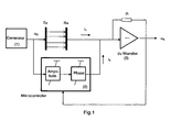
- Fig.1 a scheme is shown which illustrates the essential features of the inventive concept and also the functions of the method.
- ⁇ 0.1 results in a 9-times higher sensitivity of the sensor.
- An expedient practical implementation of the method is to realize the compensation channel largely by means of a microcontroller with integrated analog / digital and digital / analog converters, since hereby the tasks of the amplitude and phase adaptation to the measurement signal can be solved most flexibly via the software.
- adjustments to time-variant systems can thereby be carried out relatively easily, as occur, for example, in the case of movements of the transmitting and receiving electrodes relative to one another.
- the zero balance can also be automated.
- the method according to the invention also offers the advantage of working with significantly longer sensor electrodes and, if necessary, dispensing with electrode segmentation, which means a considerable simplification and cost savings in the production process of such sensor systems.
- FIG. 3 is an application example for the realization of a security example used as a burglar alarm illustrated.
- the transmitting and / or receiving electrodes which are preferably incorporated in the stationary window stock, may consist of a line segment or be segmented.
- the electrodes may be arranged in a loop and be subjected to a measuring current, which is used to detect line breaks (defect, sabotage, ).
- the electronics can optionally be mains powered and / or battery operated (e.g., power failure) and / or powered by batteries.
- the energy supply for charging the batteries and / or the operation of the electronics can optionally be done via a field coupling mechanism (E-field, H-field).
- a metal core typically present for static reasons can be used as a ground reference for the electronics.
- the ground reference can be made over metal foils which are suitably integrated in the frame.
- the earth potential / protective conductor potential can serve as a ground reference for the electronics.
- the electrodes and the electronics are preferably housed only in the frame (no moving line to the wing).
- the alarm message can be made acoustically and / or by radio and / or via a message line.
- the generator AC voltage is applied to the transmitting electrode 1.
- a capacitive current (90 ° leading) couples to the receiving electrode n.
- the capacitive current is converted into a 90 ° leading and inverted voltage.
- This voltage is added to a voltage which is also preceded by Cv by 90 ° and multiplied by a factor v.
Landscapes
- Physics & Mathematics (AREA)
- General Physics & Mathematics (AREA)
- Geophysics And Detection Of Objects (AREA)
- Investigating Or Analyzing Materials By The Use Of Electric Means (AREA)
Description
- Die Erfindung richtet sich auf ein Verfahren und eine Schaltung zur Erfassung der Annäherung eines Objektes, insbesondere einer Person an eine Elektrodeneinrichtung auf Grundlage feldelektrischer Wechselwirkungseffekte gemäß dem Oberbegriff von Patentanspruch 1.
- Aus
US 6,366,099 B1 ist eine Schaltungseinrichtung bekannt durch welche die Kapazitätsdifferenz von zwei Kondensatorsystemen erfasst wird gemäß dem Oberbegriff der Ansprüche 1 und 5. Hierbei werden die beiden Kondensatorsysteme durch einen Rechteckgenerator und jeweils eine Vorschaltdiode gegenpolig geladen. Die Ladungsdifferenz der Kondensatorsysteme wird über eine Widerstandsmessbrücke gemessen. Der Spannungspegel der Messbrücke wird über einen Operationsverstärker geführt. An den Eingang des Operationsverstärkers und damit auch an den Mittelpunkt der Messbrücke wird über parallel angeordnete R/C Glieder das Ausgangssignal des Operationsverstärkers zurückgeführt. - Aus
US 3,826,979 A ist ein als Regen-Detektor vorgesehene Streufeldsensoreinrichtung bekannt. Diese umfasst drei Elektroden. Die erste dieser Elektroden fungiert als Feldemissionselektrode und ist an einen Wechselspannungsgenerator angebunden. Die zweite Elektrode bildet eine Absorptionselektrode welche das Hauptgegenpotential zur Feldemissionselektrode bildet. Die dritte Elektrode bildet die eigentliche Sensorelektrode. Diese Sensorelektrode wird dann ausgeprägt von dem seitens der Feldemissionselektrode emittierten Feld erfasst, wenn Regentropfen auf eine mit der Sensoreinrichtung ausgestattete Windschutzscheibe treffen. Bei dieser Schaltung wird die Differenz zwischen der Spannung des Wechselspannungsgenerators und der Spannung an der Sensorelektrode erfasst und durch einen Operationsverstärker zu einem Ausgangssignal konvertiert. - Aus
US 4,016,490 ist eine weitere Sensoreinrichtung bekannt, die in ihrem Aufbau der Schaltung nachUS 3,826,979 A ähnlich ist, wobei die dort vorgesehene Gruppe aus drei Elektroden der Erfassung einer Fingerkuppe dient. - Der Erfindung liegt die Aufgabe zugrunde, Lösungen zu schaffen durch welche die Annäherung eines Objektes an eine Elektrodeneinrichtung in einer gegenüber anderweitigen Störeinflüssen relativ unempfindlichen Weise bewerkstelligt werden kann.
- Diese Aufgabe wird gemäß einem ersten Aspekt der vorliegenden Erfindung durch eine Schaltung mit den in Patentanspruch 1 angegebenen Merkmalen gelöst.
- Durch den erfindungsgemäßen Ansatz wird es auf vorteilhafte Weise möglich, bei einer hohen Sensorempfindlichkeit einer Übersteuerung der an die Empfangselektrodeneinrichtung angebundenen Schaltung vorzubeugen.
- Vorteilhafte Ausgestaltungen dieser Schaltung sind Gegenstand der Unteransprüche.
- Weitere Einzelheiten und Merkmale der Erfindung ergeben sich aus der nachfolgenden Beschreibung in Verbindung mit der Zeichnung. Es zeigt:
- Fig. 1
- eine Schemadarstellung zur Veranschaulichung des Grundaufbaus einer erfindungsgemäßen Sensorschaltung;
- Fig. 2
- eine Grafik zur Veranschaulichung der durch den Teilstrom i2 in den Proportionalbereich verlagerten Auswertungsspannung;
- Fig. 3
- eine Schemadarstellung zur Veranschaulichung eines Anwendungsbeispiels der erfindungsgemäßen Schaltung bei einer Fenstersicherung;
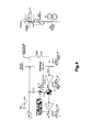
- Fig.4
- eine Schemadarstellung zur weiteren Veranschaulichung der erfindungsgemäßen Generierung eines Ausgangssignales bei einer Näherungssensoreinrichtung, insbesondere einer Fenstersicherung.
- Das erfindungsgemäße Konzept basiert auf einem Verfahren bei welchem zwischen einer Sendeelektrode (Tx) und einer Empfangselektrode (Rx) eine elektrisches Wechselfeld im Frequenzbereich von vorzugsweise 80 bis 150 kHz erzeugt wird. Taucht der leitende Gegenstand, z.B. ein Körperteil in dieses Feld zwischen den Elektroden ein, so kommt es zu einer teilweisen Absorption des Feldes über diesen Körper und damit zu einer Abschwächung eines Empfangssignales, das über einen an der Empfangselektrode angeschlossenen Verstärker gewonnen wird. Die hierbei entstehende absolute Signaländerung am Empfängerausgang ist direkt proportional zu der an der Sendeelektrode Tx anliegenden Amplitude des von einem Generator erzeugten Trägers.
- Um eine möglichst große Signaländerung und damit hohe Sensorempfindlichkeit bei Annäherung zu erreichen, wird die Generatorspannung möglichst groß eingestellt. Eine Begrenzung hierfür war bisher durch eine prinzipiell eingeschränkte Aussteuerbarkeit einer auf der Empfängerseite angeschlossenen Verstärkerstufe gegeben.
- In
Figur 2 ist der Verlauf einer Kennlinie dargestellt die den Zusammenhang zwischen einem Eingangsstrom und der Ausgangsspannung zeigt. Hierbei ist der Eingangsstrom proportional zur Generatorspannung . - Im Bereich relativ kleiner Eingangsströme ergibt sich ein linearer Zusammenhang, der bei Erreichen einer Maximalspannung eine Begrenzung erfährt. Nur im lineraren Bereich lässt sich eine Änderung des Eingangsstromes detektieren.
- Durch das erfindungsgemäße Konzept wird es möglich selbst bei einem Signalstrom bzw. einer Generatorspannung weit oberhalb des Begrenzungsbereiches die Signaländerung im linearen Bereich zu halten, wodurch eine wesentlich höhere Sensorempfindlichkeit erreicht wird.
- In
Fig.1 ist ein Schema dargestellt, das die wesentlichen Merkmale des erfindungsgemäßen Konzeptes und auch die Funktionen des Verfahrens veranschaulicht. - Ein Generator (1) erzeugt ein Trägersignal uG im Frequenzbereich 80 kHz bis 150 kHz . Dieses Signal liegt einerseits an der Sendeelektrode Tx und zum anderen am Eingang einer Kompensationsstufe (2) an, mit der die Amplitude und Phasenlage eines Kompensationssignales eingestellt werden kann, das als Teilstrom i2 mit dem von der Empfangselektrode Rx gelieferten Signalstrom i1 den Eingangsstrom i=i1+i2 für einen folgenden StromSpannungswandler (3) bildet, an dessen Ausgang dann eine Spannung entsteht

- Es ergeben sich weiter folgende Zusammenhänge zwischen den eingeführten Größen, bei denen lediglich die Betragswerte (Amplituden) betrachten werden. Es wird ferner vorausgesetzt, dass zwischen i1 und i2 außer einer Phasenverschiebung von 180° keinerlei sonstigen Phasenabweichungen zusätzlich vorhanden sind, was durch einen geeigneten Abgleich erreicht werden kann. Mit einem Absorptionskoeffizienten α, der die relative Signaländerung durch die Feldabsorption gegenüber dem Grundzustand beschreibt, erhält man dann


worin k1 und k2 Proportionalitätsfaktoren für die Amplituden sind. Damit wird GI.1 zu
- Eine maximale Kompensation ergibt sich dann für k1 = k2, womit sich dann für Gl.4 ergibt

- Es sei uG1 die für Erreichen einer maximalen Ausgangsspannung umax (sh.
Fig.2 ) erforderliche Sendspannung im unkompensierten Fall ( k2 = 0). Hierfür folgt aus Gl.4
- Für den kompensierten Fall entsprechend Gl.5 folgt dann

- Das Verhältnis der Sendespannungen in beiden Fällen repräsentiert die Erhöhung der Empfindlichkeit , da der zulässige Signalstrom i1 und damit auch dessen Änderungen proportional zu uG ist, wie bereits erläutert wurde. Dies beträgt mit den Gln. (6) und (7)

- Für z.B. α = 0,1 ergibt sich eine 9-fach höhere Empfindlickeit des Sensors.
- Eine zweckmäßige praktische Umsetzung des Verfahrens besteht darin, den Kompensationskanal weitgehend mittels eines Mikrocontrollers mit integrierten Analog/ Digital- und Digital/Analog Convertern zu realisieren, da hiermit die Aufgaben der Amplituden- und Phasenanpassung an das Messsignal am flexibelsten über die Software gelöst werden können. Insbesondere können hiermit relativ leicht Anpassungen an zeitvariante Systeme durchgeführt werden, wie sie z.B. bei Bewegungen der Sende - und Empfangselektroden zueinander auftreten. Hier ist es erforderlich, das Kompensationssignal im gleichen Maße zu verändern wie sich das Sensorsignal ändert. Durch Rückführung des Ausgangssignales des i/u-Wandlers zum Mikrocontroller (s.
Fig.1 ) kann so der Nullabgleich auch automatisiert werden. - Neben der beschriebenen Erhöhung der Sensorempfindlickeit bietet das erfindungsgemäße Verfahren auch den Vorteil, mit deutlich längeren Sensorelektroden zu arbeiten und ggf. auf eine Elektrodensegmentierung zu verzichten, was eine wesentliche Vereinfachung und Kosteneinsparung beim Produktionsprozess solcher Sensorsysteme bedeutet.
- In
Figur 3 ist ein Anwendungsbeispiel zur Realisierung einer beispielsweise als Einbruchssicherung verwendeten Fenstersicherung dargestellt. Die vorzugsweise in den stationären Fensterstock eingebundenen Sende und/oder Empfangselektroden können aus einem Leitungsstück bestehen oder segmentiert sein. - Es ist möglich, die Signale durch Abfrage mehrerer Elektroden (1.. n) zu generieren und die Relation der Signale untereinander neben der Alarmerkennung auch dazu zu verwenden, Umwelteinflüsse und Driften zu kompensieren.
- Die Elektroden können schleifenförmig angeordnet sein und mit einem Messstrom beaufschlagt werden, der zur Erkennung von Leitungsbrüchen (Defekt, Sabotage,...) dient.
- Die Elektronik kann wahlweise netzbetrieben und/oder batteriebetrieben (z.B. Netzausfall) und/oder mit Akkumulatoren betrieben werden.
- Die Energiezuführung zur Ladung der Akkumulatoren und/oder dem Betrieb der Elektronik kann wahlweise über einen Feldkoppelmechanismus (E-Feld, H-Feld) erfolgen.
- Ein im Rahmen typischerweise aus statischen Gründen vorhandener Metallkern kann als Massebezug für die Elektronik verwendet werden. Optional kann der Massebezug über Metallfolien hergestellt werden, die in geeigneter Weise im Rahmen integriert werden. Als Massebezug für die Elektronik kann das Erdpotential/Schutzleiterpotential dienen.
- Die Elektroden und die Elektronik ist bevorzugt nur im Rahmen untergebracht (keine bewegte Leitung zum Flügel). Die Alarmmeldung kann akustisch und/oder über Funk und/oder über eine Meldeleitung erfolgen.
- Wie aus der Schaltungsskizze nach
Figur 4 ersichtlich, liegt die Generatorwechselspannung an der Sende-Elektrode 1 an. Ein kapazitiver Strom (90° voreilend) koppelt auf die Empfangselektrode n. Über einen ((-I/U)-Wandler) wird der kapazitive Strom in eine um 90° voreilende und invertierte Spannung umgesetzt. Diese Spannung wird zu einer durch Cv ebenfalls um 90° voreilende und mit einem Faktor v multiplizierte Spannung addiert. Durch Regelung von v kann im Abgleichzustand (ΔC=O) die Ausgangsspannung Uout auf ein Minimum (ideal=0) reduziert werden. - Abgeglichener Zustand:
- Bei Kapazitätsänderung AC wird die Amplitude des kapazitiven Stroms verändert (is). Nach dem Addierglied (+) bleibt von der Ausgangsspannung des (-I/U)-Wandlers nur eine der Kapazitätsänderung AC proportionale Spannungsamplitude übrig. Diese kann durch den nachfolgenden Verstärker Vi - ohne diesen zu übersteuern - verstärkt werden.
Claims (6)
- Schaltung zur Generierung eines hinsichtlich der Annäherung eines Objekts an einen Observationsbereich indikativen Signales, mit- einer Sendeelektrodeneinrichtung (Tx),- einer Generatorschaltung (1) zur Beaufschlagung der Sendeelektrodeneinrichtung (Tx) mit einer Wechselspannung;- einer Empfangselektrodeneinrichtung (Rx) die sich in, oder entlang des Observationsbereiches erstreckt,- einer Ausgangsschaltung (3), zur Generierung eines mit dem an der Empfangselektrodeneinrichtung (Rx) anliegenden Feld korrelierenden Ausgangssignales (UA), und
einer Kompensationsschaltung (2), zur Addition eines Kompensationsstromes (i2) zu einem von der Empfangselektrodeneinrichtung (Rx) fließenden Signalstrom (i1), wobei der Kompensationsstrom (i2) derart eingespeist wird, dass dessen Phasenverschiebung gegenüber dem Signalstrom (i1) im Bereich von 180° liegt,
dadurch gekennzeichnet,- dass die Amplitude des Kompensationsstroms (i2) nach Maßgabe des Ausgangssignales (UA) abgestimmt wird. - Schaltung nach Anspruch 1, dadurch gekennzeichnet, dass die Kompensationsschaltung (2) über die Generatorspannung (UG) getriggert wird.
- Schaltung nach wenigstens einem der Ansprüche 1 oder 2, dadurch gekennzeichnet, dass die Ausgangssschaltung (3) als I/U Wandler ausgeführt ist.
- Schaltung nach wenigstens einem der Ansprüche 1 bis 3, dadurch gekennzeichnet, dass die Kompensationsschaltung (2) als Microcontroller ausgeführt ist.
- Verfahren zur Generierung eines hinsichtlich der Annäherung eines Objekts an einen Observationsbereich indikativen Signales, bei welchem- eine Sendeelektrodeneinrichtung mittels einer Generatorschaltung mit einer Wechselspannung beaufschlagt wird,- von einer Empfangselektrodeneinrichtung die sich in, oder entlang des Observationsbereiches erstreckt, ein Signalstrom abgegriffen, und- mittels einer Ausgangsschaltung, ein mit dem an der Empfangselektrodeneinrichtung anliegenden Feld korrelierendes Ausgangssignal erzeugt wird,- wobei mittels einer Kompensationsschaltung ein Kompensationsstrom (i2) zu einem von der Empfangselektrodeneinrichtung fließenden Signalstrom addiert wird, wobei der Kompensationsstrom (i2) derart eingespeist wird, dass dessen Phasenverschiebung gegenüber dem Signalstrom (i1) im Bereich von 180° liegt- dadurch gekennzeichnet, dass die Amplitude des Kompensationsstroms nach Maßgabe des Ausgangssignales abgestimmt wird,
- Verfahren nach Anspruch 5, dadurch gekennzeichnet, dass das Ausgangssignal anhand eines mit der Empfangselektrodeneinrichtung gekoppelten Wandlers generiert wird.
Applications Claiming Priority (2)
| Application Number | Priority Date | Filing Date | Title |
|---|---|---|---|
| DE102007043629 | 2007-09-13 | ||
| PCT/EP2008/007662 WO2009062562A1 (de) | 2007-09-13 | 2008-09-15 | Verfahren und schaltung zur detektion einer annäherung and eine elektrodeneinrichtung |
Publications (2)
| Publication Number | Publication Date |
|---|---|
| EP2220767A1 EP2220767A1 (de) | 2010-08-25 |
| EP2220767B1 true EP2220767B1 (de) | 2013-09-04 |
Family
ID=40433836
Family Applications (1)
| Application Number | Title | Priority Date | Filing Date |
|---|---|---|---|
| EP08849634.4A Active EP2220767B1 (de) | 2007-09-13 | 2008-09-15 | Verfahren und schaltung zur detektion einer annäherung an eine elektrodeneinrichtung |
Country Status (4)
| Country | Link |
|---|---|
| US (1) | US8148999B2 (de) |
| EP (1) | EP2220767B1 (de) |
| DE (1) | DE102008047434B4 (de) |
| WO (1) | WO2009062562A1 (de) |
Families Citing this family (6)
| Publication number | Priority date | Publication date | Assignee | Title |
|---|---|---|---|---|
| DE102009057933B3 (de) * | 2009-12-11 | 2011-02-24 | Ident Technology Ag | Sensoreinrichtung sowie Verfahren zur Annäherungs- und Berührungsdetektion |
| DE102011004622B4 (de) * | 2011-02-23 | 2013-04-18 | Ident Technology Ag | Kapazitive Sensoreinrichtung und Funkgerät mit kapazitiver Sensoreinrichtung sowie Verfahren zum Einstellen einer Sendeleistung eines Funkgerätes |
| CN103630748B (zh) * | 2013-11-11 | 2016-03-30 | 西安交通大学 | 一种用于微型电网谐波阻抗测量的装置及方法 |
| CN103630749B (zh) * | 2013-11-11 | 2016-01-20 | 西安交通大学 | 一种用于电网谐波阻抗测量的谐波注入装置 |
| DE102014216246A1 (de) | 2014-08-15 | 2016-02-18 | Mayser Gmbh & Co. Kg | Schaltung und Verfahren zum Auswerten von Messsignalen sowie Sensorsystem zum kapazitiven Erfassen von Hindernissen |
| FR3068814B1 (fr) * | 2017-07-05 | 2020-10-09 | Damien Koblensky | Procede et dispositif de detection d'intrusions |
Family Cites Families (11)
| Publication number | Priority date | Publication date | Assignee | Title |
|---|---|---|---|---|
| USRE25100E (en) | 1954-04-13 | 1961-12-19 | chapin | |
| DE2239359A1 (de) | 1972-08-10 | 1974-02-21 | Bosch Gmbh Robert | Schaltanordnung mit einem kapazitiven detektor |
| DE2460057B2 (de) * | 1974-12-19 | 1977-02-10 | Robert Bosch Gmbh, 7000 Stuttgart | Schaltanordnung mit einem streufeldkondensator |
| US4071820A (en) | 1976-04-05 | 1978-01-31 | Alton Corporation | Measurement system |
| US5670886A (en) | 1991-05-22 | 1997-09-23 | Wolf Controls Corporation | Method and apparatus for sensing proximity or position of an object using near-field effects |
| DE19549314A1 (de) * | 1995-12-29 | 1997-07-03 | Richard Prof Dr Schimko | Elektronisches Überwachungssystem |
| US6366099B1 (en) | 1999-12-21 | 2002-04-02 | Conrad Technologies, Inc. | Differential capacitance sampler |
| DE19963773C2 (de) * | 1999-12-30 | 2003-07-24 | Secon Gmbh | Metalldetektor und Verfahren zum Betreiben eines Metalldetektors |
| DE102004047190A1 (de) * | 2004-09-29 | 2006-04-06 | Robert Bosch Gmbh | Detektor zur Ortung metallischer Objekte |
| DE102007026307A1 (de) * | 2006-06-06 | 2008-02-07 | Ident Technology Ag | Anordnung zur Generierung eines für die Präsenz eines Objektes innerhalb eines Observationsbereiches indikativen Signals |
| DE102007001688A1 (de) * | 2007-01-11 | 2008-10-30 | Ident Technology Ag | Anordnung zur Detektion von Körperteilen mittels Absorption eines elektrischen Nahfeldes |
-
2008
- 2008-09-15 WO PCT/EP2008/007662 patent/WO2009062562A1/de not_active Ceased
- 2008-09-15 DE DE102008047434.7A patent/DE102008047434B4/de active Active
- 2008-09-15 EP EP08849634.4A patent/EP2220767B1/de active Active
- 2008-09-15 US US12/446,657 patent/US8148999B2/en active Active
Also Published As
| Publication number | Publication date |
|---|---|
| DE102008047434A1 (de) | 2009-05-20 |
| DE102008047434B4 (de) | 2017-03-16 |
| US20110062963A1 (en) | 2011-03-17 |
| EP2220767A1 (de) | 2010-08-25 |
| WO2009062562A1 (de) | 2009-05-22 |
| US8148999B2 (en) | 2012-04-03 |
Similar Documents
| Publication | Publication Date | Title |
|---|---|---|
| EP2220767B1 (de) | Verfahren und schaltung zur detektion einer annäherung an eine elektrodeneinrichtung | |
| DE10131243C1 (de) | Kapazitiver Näherungsschalter | |
| DE102011008277B4 (de) | Sensoreinheit zum berührungslosen Betätigen einer Fahrzeugtür | |
| EP1943734B1 (de) | Schaltung zur erfassung der präsenz, position und/oder annäherung eines objektes an wenigstens eine elektrodeneinrichtung | |
| DE19701899C2 (de) | Schaltungsanordnung und Verfahren zur Erfassung der Kapazität bzw. einer Kapazitätsänderung eines kapazitiven Schaltungs- oder Bauelementes | |
| DE112014001890B4 (de) | Kapazitive Erfassungsvorrichtung | |
| WO2007012502A9 (de) | Verfahren und vorrichtung zur entfernungsmessung mittels kapazitiven oder induktiven sensoren | |
| EP2389564A1 (de) | Verfahren zum induktiven erzeugen eines elektrischen messsignals sowie zugehörige sensorvorrichtung | |
| EP2494382A1 (de) | Vorrichtung und verfahren zur fehlerfreien kapazitiven messwerterfassung | |
| EP2555019B1 (de) | Induktiver Näherungssensor | |
| EP2651036A1 (de) | Induktiver Näherungssensor | |
| EP0359797A1 (de) | Einklemmschutz | |
| DE102007026307A1 (de) | Anordnung zur Generierung eines für die Präsenz eines Objektes innerhalb eines Observationsbereiches indikativen Signals | |
| DE102012019329A1 (de) | Verfahren und Sensoreinheit zur Ortung und/oder Erkennung metallischer oder Metall enthaltender Objekte und Materalien | |
| DE102007001712B4 (de) | Anordnung zur Generierung eines für die Präsenz eines Objektes innerhalb eines Observationsbereiches indikativen Signals | |
| EP2159600A1 (de) | Elektro-optischer Detektor zur Erkennung des Vorhandenseins und/oder der Annäherung eines Objekts | |
| DE102013202573B3 (de) | Induktiver Näherungsschalter | |
| DE102019133928A1 (de) | Anordnung für ein Fahrzeug | |
| EP2642663B1 (de) | Sensor und Verfahren zum Nachweisen eines Objekts | |
| EP3824323B1 (de) | Detektor zum detektieren von elektrisch leitfähigem material | |
| EP1797394B1 (de) | Verfahren und anordnung zum bestimmen des abstandes zwischen einer profilierten oberfläche von einer sich relativ dazu bewegenden funktionsfläche mittels zweier messspulen | |
| WO2014079409A2 (de) | Drehmomentmesseinrichtung und verfahren zum messen eines drehmoments | |
| EP3667918B1 (de) | Anordnung für ein fahrzeug | |
| EP3563144B1 (de) | Verfahren zum betreiben eines kapazitiven regensensors eines kraftfahrzeugs | |
| EP4191116A1 (de) | Sicherheitseinrichtung |
Legal Events
| Date | Code | Title | Description |
|---|---|---|---|
| PUAI | Public reference made under article 153(3) epc to a published international application that has entered the european phase |
Free format text: ORIGINAL CODE: 0009012 |
|
| 17P | Request for examination filed |
Effective date: 20100614 |
|
| AK | Designated contracting states |
Kind code of ref document: A1 Designated state(s): AT BE BG CH CY CZ DE DK EE ES FI FR GB GR HR HU IE IS IT LI LT LU LV MC MT NL NO PL PT RO SE SI SK TR |
|
| AX | Request for extension of the european patent |
Extension state: AL BA MK RS |
|
| 17Q | First examination report despatched |
Effective date: 20101020 |
|
| DAX | Request for extension of the european patent (deleted) | ||
| RAP1 | Party data changed (applicant data changed or rights of an application transferred) |
Owner name: IDENT TECHNOLOGY AG |
|
| GRAP | Despatch of communication of intention to grant a patent |
Free format text: ORIGINAL CODE: EPIDOSNIGR1 |
|
| R17P | Request for examination filed (corrected) |
Effective date: 20100413 |
|
| RIC1 | Information provided on ipc code assigned before grant |
Ipc: G08B 13/08 20060101ALN20130205BHEP Ipc: H03K 17/955 20060101AFI20130205BHEP |
|
| GRAS | Grant fee paid |
Free format text: ORIGINAL CODE: EPIDOSNIGR3 |
|
| GRAA | (expected) grant |
Free format text: ORIGINAL CODE: 0009210 |
|
| RAP1 | Party data changed (applicant data changed or rights of an application transferred) |
Owner name: MICROCHIP TECHNOLOGY GERMANY II GMBH & CO. KG |
|
| AK | Designated contracting states |
Kind code of ref document: B1 Designated state(s): AT BE BG CH CY CZ DE DK EE ES FI FR GB GR HR HU IE IS IT LI LT LU LV MC MT NL NO PL PT RO SE SI SK TR |
|
| REG | Reference to a national code |
Ref country code: GB Ref legal event code: FG4D Free format text: NOT ENGLISH |
|
| REG | Reference to a national code |
Ref country code: CH Ref legal event code: EP |
|
| REG | Reference to a national code |
Ref country code: AT Ref legal event code: REF Ref document number: 630974 Country of ref document: AT Kind code of ref document: T Effective date: 20130915 |
|
| REG | Reference to a national code |
Ref country code: IE Ref legal event code: FG4D Free format text: LANGUAGE OF EP DOCUMENT: GERMAN |
|
| REG | Reference to a national code |
Ref country code: DE Ref legal event code: R096 Ref document number: 502008010615 Country of ref document: DE Effective date: 20131031 |
|
| REG | Reference to a national code |
Ref country code: NL Ref legal event code: T3 |
|
| PG25 | Lapsed in a contracting state [announced via postgrant information from national office to epo] |
Ref country code: LT Free format text: LAPSE BECAUSE OF FAILURE TO SUBMIT A TRANSLATION OF THE DESCRIPTION OR TO PAY THE FEE WITHIN THE PRESCRIBED TIME-LIMIT Effective date: 20130904 Ref country code: NO Free format text: LAPSE BECAUSE OF FAILURE TO SUBMIT A TRANSLATION OF THE DESCRIPTION OR TO PAY THE FEE WITHIN THE PRESCRIBED TIME-LIMIT Effective date: 20131204 Ref country code: SE Free format text: LAPSE BECAUSE OF FAILURE TO SUBMIT A TRANSLATION OF THE DESCRIPTION OR TO PAY THE FEE WITHIN THE PRESCRIBED TIME-LIMIT Effective date: 20130904 Ref country code: CY Free format text: LAPSE BECAUSE OF FAILURE TO SUBMIT A TRANSLATION OF THE DESCRIPTION OR TO PAY THE FEE WITHIN THE PRESCRIBED TIME-LIMIT Effective date: 20130904 Ref country code: HR Free format text: LAPSE BECAUSE OF FAILURE TO SUBMIT A TRANSLATION OF THE DESCRIPTION OR TO PAY THE FEE WITHIN THE PRESCRIBED TIME-LIMIT Effective date: 20130904 |
|
| REG | Reference to a national code |
Ref country code: LT Ref legal event code: MG4D |
|
| PG25 | Lapsed in a contracting state [announced via postgrant information from national office to epo] |
Ref country code: SI Free format text: LAPSE BECAUSE OF FAILURE TO SUBMIT A TRANSLATION OF THE DESCRIPTION OR TO PAY THE FEE WITHIN THE PRESCRIBED TIME-LIMIT Effective date: 20130904 Ref country code: PL Free format text: LAPSE BECAUSE OF FAILURE TO SUBMIT A TRANSLATION OF THE DESCRIPTION OR TO PAY THE FEE WITHIN THE PRESCRIBED TIME-LIMIT Effective date: 20130904 Ref country code: LV Free format text: LAPSE BECAUSE OF FAILURE TO SUBMIT A TRANSLATION OF THE DESCRIPTION OR TO PAY THE FEE WITHIN THE PRESCRIBED TIME-LIMIT Effective date: 20130904 Ref country code: GR Free format text: LAPSE BECAUSE OF FAILURE TO SUBMIT A TRANSLATION OF THE DESCRIPTION OR TO PAY THE FEE WITHIN THE PRESCRIBED TIME-LIMIT Effective date: 20131205 Ref country code: FI Free format text: LAPSE BECAUSE OF FAILURE TO SUBMIT A TRANSLATION OF THE DESCRIPTION OR TO PAY THE FEE WITHIN THE PRESCRIBED TIME-LIMIT Effective date: 20130904 Ref country code: ES Free format text: LAPSE BECAUSE OF FAILURE TO SUBMIT A TRANSLATION OF THE DESCRIPTION OR TO PAY THE FEE WITHIN THE PRESCRIBED TIME-LIMIT Effective date: 20130904 |
|
| BERE | Be: lapsed |
Owner name: MICROCHIP TECHNOLOGY GERMANY II G.M.B.H. & CO. KG Effective date: 20130930 |
|
| PG25 | Lapsed in a contracting state [announced via postgrant information from national office to epo] |
Ref country code: RO Free format text: LAPSE BECAUSE OF FAILURE TO SUBMIT A TRANSLATION OF THE DESCRIPTION OR TO PAY THE FEE WITHIN THE PRESCRIBED TIME-LIMIT Effective date: 20130904 Ref country code: EE Free format text: LAPSE BECAUSE OF FAILURE TO SUBMIT A TRANSLATION OF THE DESCRIPTION OR TO PAY THE FEE WITHIN THE PRESCRIBED TIME-LIMIT Effective date: 20130904 Ref country code: CZ Free format text: LAPSE BECAUSE OF FAILURE TO SUBMIT A TRANSLATION OF THE DESCRIPTION OR TO PAY THE FEE WITHIN THE PRESCRIBED TIME-LIMIT Effective date: 20130904 Ref country code: IS Free format text: LAPSE BECAUSE OF FAILURE TO SUBMIT A TRANSLATION OF THE DESCRIPTION OR TO PAY THE FEE WITHIN THE PRESCRIBED TIME-LIMIT Effective date: 20140104 Ref country code: SK Free format text: LAPSE BECAUSE OF FAILURE TO SUBMIT A TRANSLATION OF THE DESCRIPTION OR TO PAY THE FEE WITHIN THE PRESCRIBED TIME-LIMIT Effective date: 20130904 |
|
| REG | Reference to a national code |
Ref country code: CH Ref legal event code: PL |
|
| REG | Reference to a national code |
Ref country code: DE Ref legal event code: R097 Ref document number: 502008010615 Country of ref document: DE |
|
| PG25 | Lapsed in a contracting state [announced via postgrant information from national office to epo] |
Ref country code: PT Free format text: LAPSE BECAUSE OF FAILURE TO SUBMIT A TRANSLATION OF THE DESCRIPTION OR TO PAY THE FEE WITHIN THE PRESCRIBED TIME-LIMIT Effective date: 20140106 Ref country code: MC Free format text: LAPSE BECAUSE OF FAILURE TO SUBMIT A TRANSLATION OF THE DESCRIPTION OR TO PAY THE FEE WITHIN THE PRESCRIBED TIME-LIMIT Effective date: 20130904 |
|
| REG | Reference to a national code |
Ref country code: IE Ref legal event code: MM4A |
|
| PLBE | No opposition filed within time limit |
Free format text: ORIGINAL CODE: 0009261 |
|
| STAA | Information on the status of an ep patent application or granted ep patent |
Free format text: STATUS: NO OPPOSITION FILED WITHIN TIME LIMIT |
|
| PG25 | Lapsed in a contracting state [announced via postgrant information from national office to epo] |
Ref country code: LI Free format text: LAPSE BECAUSE OF NON-PAYMENT OF DUE FEES Effective date: 20130930 Ref country code: IE Free format text: LAPSE BECAUSE OF NON-PAYMENT OF DUE FEES Effective date: 20130915 Ref country code: BE Free format text: LAPSE BECAUSE OF NON-PAYMENT OF DUE FEES Effective date: 20130930 Ref country code: CH Free format text: LAPSE BECAUSE OF NON-PAYMENT OF DUE FEES Effective date: 20130930 |
|
| 26N | No opposition filed |
Effective date: 20140605 |
|
| PG25 | Lapsed in a contracting state [announced via postgrant information from national office to epo] |
Ref country code: IT Free format text: LAPSE BECAUSE OF FAILURE TO SUBMIT A TRANSLATION OF THE DESCRIPTION OR TO PAY THE FEE WITHIN THE PRESCRIBED TIME-LIMIT Effective date: 20130904 |
|
| REG | Reference to a national code |
Ref country code: DE Ref legal event code: R097 Ref document number: 502008010615 Country of ref document: DE Effective date: 20140605 |
|
| PG25 | Lapsed in a contracting state [announced via postgrant information from national office to epo] |
Ref country code: DK Free format text: LAPSE BECAUSE OF FAILURE TO SUBMIT A TRANSLATION OF THE DESCRIPTION OR TO PAY THE FEE WITHIN THE PRESCRIBED TIME-LIMIT Effective date: 20130904 |
|
| REG | Reference to a national code |
Ref country code: AT Ref legal event code: MM01 Ref document number: 630974 Country of ref document: AT Kind code of ref document: T Effective date: 20130915 |
|
| PG25 | Lapsed in a contracting state [announced via postgrant information from national office to epo] |
Ref country code: AT Free format text: LAPSE BECAUSE OF NON-PAYMENT OF DUE FEES Effective date: 20130915 |
|
| PG25 | Lapsed in a contracting state [announced via postgrant information from national office to epo] |
Ref country code: MT Free format text: LAPSE BECAUSE OF FAILURE TO SUBMIT A TRANSLATION OF THE DESCRIPTION OR TO PAY THE FEE WITHIN THE PRESCRIBED TIME-LIMIT Effective date: 20130904 Ref country code: TR Free format text: LAPSE BECAUSE OF FAILURE TO SUBMIT A TRANSLATION OF THE DESCRIPTION OR TO PAY THE FEE WITHIN THE PRESCRIBED TIME-LIMIT Effective date: 20130904 |
|
| PG25 | Lapsed in a contracting state [announced via postgrant information from national office to epo] |
Ref country code: BG Free format text: LAPSE BECAUSE OF FAILURE TO SUBMIT A TRANSLATION OF THE DESCRIPTION OR TO PAY THE FEE WITHIN THE PRESCRIBED TIME-LIMIT Effective date: 20130904 Ref country code: HU Free format text: LAPSE BECAUSE OF FAILURE TO SUBMIT A TRANSLATION OF THE DESCRIPTION OR TO PAY THE FEE WITHIN THE PRESCRIBED TIME-LIMIT; INVALID AB INITIO Effective date: 20080915 Ref country code: LU Free format text: LAPSE BECAUSE OF NON-PAYMENT OF DUE FEES Effective date: 20130915 |
|
| REG | Reference to a national code |
Ref country code: FR Ref legal event code: PLFP Year of fee payment: 9 |
|
| REG | Reference to a national code |
Ref country code: FR Ref legal event code: PLFP Year of fee payment: 10 |
|
| REG | Reference to a national code |
Ref country code: GB Ref legal event code: 732E Free format text: REGISTERED BETWEEN 20171123 AND 20171129 |
|
| REG | Reference to a national code |
Ref country code: DE Ref legal event code: R082 Ref document number: 502008010615 Country of ref document: DE Representative=s name: WESTPHAL, MUSSGNUG & PARTNER PATENTANWAELTE MI, DE Ref country code: DE Ref legal event code: R081 Ref document number: 502008010615 Country of ref document: DE Owner name: MICROCHIP TECHNOLOGY GERMANY GMBH, DE Free format text: FORMER OWNER: MICROCHIP TECHNOLOGY GERMANY II GMBH & CO. KG, 82205 GILCHING, DE |
|
| REG | Reference to a national code |
Ref country code: FR Ref legal event code: TP Owner name: MICROCHIP TECHNOLOGY GERMANY GMBH, DE Effective date: 20180622 |
|
| REG | Reference to a national code |
Ref country code: FR Ref legal event code: PLFP Year of fee payment: 11 |
|
| REG | Reference to a national code |
Ref country code: NL Ref legal event code: PD Owner name: MICROCHIP TECHNOLOGY GERMANY GMBH; DE Free format text: DETAILS ASSIGNMENT: CHANGE OF OWNER(S), ASSIGNMENT; FORMER OWNER NAME: MICROCHIP TECHNOLOGY GERMANY II GMBH & CO. KG Effective date: 20190816 |
|
| P01 | Opt-out of the competence of the unified patent court (upc) registered |
Effective date: 20230528 |
|
| PGFP | Annual fee paid to national office [announced via postgrant information from national office to epo] |
Ref country code: NL Payment date: 20250820 Year of fee payment: 18 |
|
| PGFP | Annual fee paid to national office [announced via postgrant information from national office to epo] |
Ref country code: DE Payment date: 20250820 Year of fee payment: 18 |
|
| PGFP | Annual fee paid to national office [announced via postgrant information from national office to epo] |
Ref country code: GB Payment date: 20250822 Year of fee payment: 18 |
|
| PGFP | Annual fee paid to national office [announced via postgrant information from national office to epo] |
Ref country code: FR Payment date: 20250820 Year of fee payment: 18 |