EP2221173A1 - Film composite électroluminescent doté d'un laminé à film protecteur - Google Patents
Film composite électroluminescent doté d'un laminé à film protecteur Download PDFInfo
- Publication number
- EP2221173A1 EP2221173A1 EP08020616A EP08020616A EP2221173A1 EP 2221173 A1 EP2221173 A1 EP 2221173A1 EP 08020616 A EP08020616 A EP 08020616A EP 08020616 A EP08020616 A EP 08020616A EP 2221173 A1 EP2221173 A1 EP 2221173A1
- Authority
- EP
- European Patent Office
- Prior art keywords
- layers
- protective film
- layer
- film laminate
- electroluminescent
- Prior art date
- Legal status (The legal status is an assumption and is not a legal conclusion. Google has not performed a legal analysis and makes no representation as to the accuracy of the status listed.)
- Ceased
Links
Images
Classifications
-
- B—PERFORMING OPERATIONS; TRANSPORTING
- B32—LAYERED PRODUCTS
- B32B—LAYERED PRODUCTS, i.e. PRODUCTS BUILT-UP OF STRATA OF FLAT OR NON-FLAT, e.g. CELLULAR OR HONEYCOMB, FORM
- B32B27/00—Layered products comprising a layer of synthetic resin
- B32B27/06—Layered products comprising a layer of synthetic resin as the main or only constituent of a layer, which is next to another layer of the same or of a different material
-
- B—PERFORMING OPERATIONS; TRANSPORTING
- B32—LAYERED PRODUCTS
- B32B—LAYERED PRODUCTS, i.e. PRODUCTS BUILT-UP OF STRATA OF FLAT OR NON-FLAT, e.g. CELLULAR OR HONEYCOMB, FORM
- B32B7/00—Layered products characterised by the relation between layers; Layered products characterised by the relative orientation of features between layers, or by the relative values of a measurable parameter between layers, i.e. products comprising layers having different physical, chemical or physicochemical properties; Layered products characterised by the interconnection of layers
- B32B7/04—Interconnection of layers
- B32B7/06—Interconnection of layers permitting easy separation
-
- B—PERFORMING OPERATIONS; TRANSPORTING
- B32—LAYERED PRODUCTS
- B32B—LAYERED PRODUCTS, i.e. PRODUCTS BUILT-UP OF STRATA OF FLAT OR NON-FLAT, e.g. CELLULAR OR HONEYCOMB, FORM
- B32B7/00—Layered products characterised by the relation between layers; Layered products characterised by the relative orientation of features between layers, or by the relative values of a measurable parameter between layers, i.e. products comprising layers having different physical, chemical or physicochemical properties; Layered products characterised by the interconnection of layers
- B32B7/04—Interconnection of layers
- B32B7/12—Interconnection of layers using interposed adhesives or interposed materials with bonding properties
Definitions
- the present invention relates to an electroluminescent composite film with a protective film laminate, a process for its preparation, and their use as lighting on a motor vehicle.
- the illumination is preferably achieved by electroluminescent films, which are fastened with a single-sided adhesive tape on the racing vehicle, for example on the door (s) and / or the hood.
- the adhesive tape is preferably guided completely around the edge of the electroluminescent film, which adheres one part of the tape to the film and another part to the surface on which the film is to be fastened.
- electroluminescent films offer the advantage that they are self-luminous and can thus illuminate characters including graphics and lettering without the need for prior illumination by an external light source.
- An object of the present invention was therefore to provide an electroluminescent film composite (EL film composite) which can be cleaned quickly and effectively, that is, which can be quickly and effectively rid of dirt.
- EL film composite electroluminescent film composite
- the protective film laminate (a) comprises at least one (1) layer.
- the protective film laminate (a) comprises at least 2 layers, more preferably the protective film laminate (a) comprises at least 5 layers, most preferably the protective film laminate (a) comprises at least 10 layers, especially at least 25 layers.
- a maximum number of layers of the protective film laminate (a) is in the range between 40 and 50 layers. Depending on the application, however, a number of 1, 2, 3, 4, 5, 6, 7, 8, 9, 10, 11 or 12 layers may be useful. A low number of layers is particularly advantageous if the EL element foreseeable only a few times, for example, one, two or three or four times, must be cleaned or should.
- the protective film laminate (a) preferably covers the EL element (c) over the entire surface, whereby the entire surface of the EL element can be protected, and protrudes flat over this at its edges.
- the adhesive layer (b) on the underside of the protective film laminate (a) fixes it to the EL element. Through the parts of the protective laminate (a), which protrude over the EL element surface, the entire EL film composite is attached by means of the adhesive layer (b) on a substrate.
- the EL film composite can be applied to any surface.
- the substrate is a surface of metal, plastic, glass, wood and / or concrete, which in turn may be coated, for example with a paint, a paint, a plastic film, paper or cardboard;
- a paint, a paint, a plastic film, paper or cardboard are also possible. Examples of such a surface are doors, windows, bonnets of motor vehicles,
- Advertising columns Billboards, shop windows, walls of public transport stops, etc.
- the film composite as a whole can be produced for example by methods known to those skilled in the art, such as hot or cold laminating, placing the protective film laminate (a) including adhesive layer (b) on the EL element (c) or vice versa with the aid of pick & place machines or laminating ,
- Electroluminescence refers to the direct luminescence excitation of luminescent pigments (also called luminous substances or luminophors) through an alternating electric field.
- Information carrier advertising or transparency can serve for decorative purposes, known in the art.
- US2007 / 223211A1 For example, it is known to backlit the interior sides of a menu with at least one EL element to allow restaurant guests to read the menu even in subdued light. US2007 / 223211A1 also discloses the electronics, switchgear and power supply associated with the EL application. Among other things, the electronics make it possible to produce color changes of the EL element.
- WO2006100164A1 discloses the construction of an EL element with a substrate corresponding to substrate (ca) of polycarbonate and a certain water vapor permeability of the protective layer, corresponding to (cc), in FIG WO2006100164A1 Called protective laminate.
- Such EL elements can be almost freely deformable three-dimensional.
- the German patent application DE 10 2006 059 203 A1 discloses such an EL element.
- the element In order for this film element is three-dimensionally deformable, the element must have a specific layer structure. The deformation of the film element can then be carried out by high-pressure isostatic deformation. In the context of the present invention, the use of such three-dimensionally deformable EL elements is particularly preferred.
- the EL element may be configured such that the side of the substrate provided with the EL device is illuminated, or that an at least partially transparent substrate is illuminated by a back-mounted EL device. Furthermore, the illumination can also radiate to both sides, if the substrate is at least partially transparent.
- a protective film laminate (a) suitable for the present invention is made US 5,592,698 A . US 6,388,813 B1 . US2002 / 0109922A1 . US 6,536,045 B1 and US2003 / 0066118A1 known.
- the EL element provided according to the invention may have further layers.
- the substrate itself is electrically conductive, it may or may not be provided with an additional insulating layer to which the EL device is then applied.
- the EL element may have one or more reflective layers.
- the reflection layer preferably comprises glass beads, in particular hollow glass beads.
- the diameter of the glass beads can be changed within wide limits. Thus, they can have a size d 50 of generally 5 ⁇ m to 3 mm, preferably 10 to 200 ⁇ m, particularly preferably 20 to 100 ⁇ m.
- the hollow glass beads are preferably embedded in a binder.
- one or more at least partially transparent graphically designed layers can be arranged on the substrate and / or the substrate and the EL arrangement.
- the EL element provided according to the invention with inverse layer structure can have further layers.
- the substrate itself is electrically conductive, it may or may not be provided with an additional insulating layer to which the EL device is then applied.
- the EL element may have one or more reflective layers.
- one or more at least partially transparent graphically designed layers can be arranged on the EL arrangement, its base and / or on the protective film laminate (a).
- the one or more insulation layer (s) (cbb) and / or (cbd) both in the conventional structure and in the inverse structure can or can be omitted in particular if the component (cbc) has a layer thickness which short-circuits the two Electrode components (cba) and (cbe) prevented.
- the electrodes (cba) and (cbe) have electrical connections, which are preferably guided to a side edge of the film element according to the invention and contacted there by contacting aids with a current source.
- Suitable contacting aids are, for example, crimping, clamping, electrically conductive adhesive, rivets, screws and other means known to those skilled in the art.
- the control of the EL element can be carried out in a conventional manner known to the expert.
- the activation of the resulting EL element is effected by a capacitive energy transfer.
- the EL element according to the invention is operated by means of alternating current.
- the alternating current is preferably generated by means of an EL-DC / AC inverter.
- the inverter is conventionally mounted together with control electronics on a printed circuit board.
- the power supply can be done for example by battery (s), rechargeable accumulator (s) or by supply by an external power source.
- a power supply may be provided by the battery (s) and / or rechargeable battery (s).
- the EL element used according to the invention has a first at least partially transparent electrode, front electrode (cba), and a second back electrode (cbe).
- the expression "at least partially transparent” means an electrode which is constructed from a material which has a transmission of visible light of generally more than 60%, preferably more than 70%, particularly preferably more than 80%, especially more than 90%.
- the back electrode (cbe) of the EL arrangement which may be provided for example on the surface of the substrate, does not necessarily have to be transparent or opaque.
- Suitable electrical conductive materials for the electrodes are known per se to those skilled in the art. Basically, when producing thick-film EL elements with AC excitation (thick-film AC-EL elements), there are several types of electrodes. On the one hand, these are sputtered or vapor deposited indium-tin-oxide electrodes (indium-tin-oxides, ITO) in vacuum on plastic films. They are very thin (some 100 ⁇ ) and offer the advantage of high transparency with a relatively low surface resistance (about 60 to 600 ⁇ ).
- ITO indium-tin-oxides
- printing pastes with ITO or ATO (antimony tin oxides, antimony tin oxide) or intrinsically conductive transparent polymer pastes can be used, from which surface electrodes are produced by screen printing. At a thickness of about 5 to 20 microns such electrodes offer only lower transparency at high surface resistance (up to 50 k ⁇ ). They can be applied in virtually any structure, even on structured surfaces. Furthermore, they offer a relatively good laminatability.
- Non-ITO screen printing layers (the term "non-ITO” encompasses all screen printing layers which are not based on indium-tin-oxide (ITO)), ie intrinsically conductive polymer layers with usually nanoscale electrically conductive pigments, for example the ATO screen-printing pastes polymer polyethylene-dioxythiophene with the designations 7162E or 7164 from DuPont, intrinsically conductive polymer systems such as Orgacon ® system from Agfa, the Clevios ® poly (3,4-ethylenedioxythiophene) system from HC Starck GmbH, which (as an organic metal PEDTconductive ) system of Ormecon, conductive coating or ink systems of Panipol OY and optionally with highly flexible binders, for example based on PU (polyurethanes), PMMA (polymethyl methacrylate), PVA (polyvinyl alcohol), modified polyaniline, can be used.
- PU polyurethanes
- PMMA poly
- electrically conductive polymer films are polyanilines, polythiophenes, polyacetylenes, polypyrroles ( Handbook of Conducting Polymers, 1986 ) with and without metal oxide filling.
- a printing paste for producing the at least partially transparent electrode preference is given to 10 to 90% by weight, preferably 20 to 80% by weight, particularly preferably 30 to 65% by weight, based in each case on the total weight of Clevios P, Clevios P AG, Clevios P HCV4, Clevios P HS, Clevios PH 500, Clevios PH 510 or any mixtures thereof.
- solvents dimethylsulfoxide (DMSO), N, N-dimethylformamide, N, N-dimethylacetamide, ethylene glycol, glycerol, sorbitol, methanol, ethanol, isopropanol, N-propanol, acetone, methyl ethyl ketone, dimethylaminoethanol, water or mixtures of two or three or more of said solvents can be used.
- the amount of solvent can vary widely in the printing paste. Thus, in one formulation of a paste 55 to 60 wt .-% solvent may be included, while in another formulation, about 35 to 45 wt .-% of a solvent mixture of two or more solvents are used.
- Neo Rez R986, Dynol 604 and / or mixtures of two or more of these substances may be included.
- the amount thereof is 0.1 to 5.0 wt .-%, preferably 0.3 to 2.5 wt .-%, based on the total weight of the printing paste.
- binders which may be present in the formulation are UD-85, Bayhydrol PR340 / 1, Bayhydrol PR135 or any mixtures thereof, preferably in amounts of from about 0.5 to 10% by weight, preferably from 3 to 5% by weight.
- the polyurethane dispersions used, which form the binder for the conductive layer after the layer has been dried, are preferably aqueous polyurethane dispersions.
- Particularly preferred formulations of printing pastes according to the invention for producing the at least partially transparent electrode (cba) comprise:
- the ready-to-use formulations mentioned below can also be used according to the invention as ready-made, commercially available printing pastes: the Orgacon EL-P1000, EL-P3000, EL-P5000 or EL-P6000 series from Agfa, preferably the EL-P3000 and EL-P6000 series (especially for deformable applications).
- tin oxide (NESA) pastes are also conceivable as corresponding electrode material.
- the electrically conductive materials described above may also be applied to a substrate.
- a carrier material for example, offer transparent glasses and thermoplastic films. Corresponding carrier materials are described in more detail below. Within the scope of the present invention, one or two carrier substrates may be used
- Electrode materials can be applied, for example, by means of screen printing, knife coating, spraying, spraying, brushing onto corresponding carrier materials (substrates), preferably subsequently drying at low temperatures of, for example, 80 to 120 ° C.
- the application of the electrically conductive coating takes place by means of vacuum or pyrolytically.
- the electrically conductive coating is particularly preferably a thin and largely transparent layer which is produced by means of vacuum or pyrolytically produced metallic or metal oxide and which preferably has a sheet resistance of 5 m ⁇ to 3000 ⁇ / square, particularly preferably a sheet resistance of 0.1 to 1000 ⁇ / sq. very particularly preferably has 5 to 30 ⁇ / square, and in another preferred embodiment has a daylight transmittance of at least greater than 60% (> 60 to 100%) and in particular greater than 76% (> 76 to 100%).
- electrically conductive glass can also be used as the electrode.
- a particular preferred type of electrically conductive and highly transparent glass, in particular float glass, are pyrolytically produced layers which have a high surface hardness and whose surface electrical resistivity can be adjusted in a very wide range, generally from a few milliohms to 3000 ⁇ / square.
- Such pyrolytically coated glasses can be well deformed and have a good scratch resistance, in particular scratches do not lead to an electrical interruption of the electrically conductive surface layer, but only to a mostly slight increase in surface resistance.
- pyrolytically produced conductive surface layers are so strongly diffused into the surface by the temperature treatment and anchored in the surface, that in a subsequent application of material an extremely high adhesion to the glass substrate is given, which is also very advantageous for the present invention.
- coatings have a good homogeneity, ie a low scattering of the surface resistance value over large surfaces. This feature also provides an advantage to the present invention.
- Electrically conductive and highly transparent thin layers can be produced on a glass substrate, which is preferably used according to the invention, much more efficiently and cost-effectively than on polymeric substrates such as PET or PMMA or PC.
- the electrical surface resistance is on glass coatings on average by a factor of 10 cheaper than on a polymeric film with comparable transparency, for example, 3 to 10 ohms / square in glass layers compared with 30 to 100 ⁇ / square on PET films.
- the back electrode (cbe) is - as in the case of the at least partially transparent electrode (cba) - a planar electrode, which, however, need not be transparent or at least partially transparent. This is generally applied to the insulating layer, if present. If no insulation layer is present, the back electrode is applied to the layer containing at least one excitable by an electric field luminous substance. In an alternative embodiment, the back electrode is applied to the at least partially transparent substrate (ca).
- the back electrode is generally constructed of inorganic or organic based electrically conductive materials such as metals such as silver, preferably using those materials that are not damaged when using the high pressure isostatic forming process to produce the three-dimensionally deformed EL element.
- Suitable electrodes are also in particular polymeric electrically conductive coatings. In this case, the coatings already mentioned above with regard to the at least partially transparent electrode can be used. In addition, it is possible to use those polymeric, electrically conductive coatings which are known to the person skilled in the art and which are not at least partially transparent.
- Suitable materials of the back electrode are thus preferably selected from the group consisting of metals such as silver, carbon, ITO screen printing layers, ATO screen printing layers, non-ITO screen printing layers, ie intrinsically conductive polymeric systems with usually nanoscale electrically conductive pigments, for example ATO dyes.
- the formulation of the print paste for the back electrode may correspond to that of the partially transparent electrode.
- a printing paste for the production of the back electrode 30 to 90% by weight, preferably 40 to 80% by weight, particularly preferably 50 to 70% by weight, based in each case on the total weight of the printing paste, of the conductive polymer Clevios P, Clevios PH, Clevios P AG, Clevios P HCV4, Clevios P HS, Clevios PH, Clevios PH 500, Clevios PH 510 or any mixtures thereof.
- solvents dimethyl sulfoxide (DMSO), N, N-dimethylformamide, N, N-dimethylacetamide, ethylene glycol, glycerol, sorbitol, methanol, ethanol, Isopropanol, N-propanol, Acton, methyl ethyl ketone, dimethylaminoethanol, water or mixtures of two or three or more of these solvents may be used.
- the amount of solvent used can vary widely. Thus, in a formulation according to the invention, one paste may contain from 55 to 60% by weight of solvent, while in another formulation according to the invention about 40% by weight of a solvent mixture of three solvents may be used.
- Neo Rez R986, Dynol 604 or mixtures of two or more of these substances may preferably be contained in an amount of 0.7 to 1.2 wt .-%.
- binders for example, 0.5 to 1.5 wt .-% UD-85, Bayhydrol PR340 / 1, Bayhydrol PR135 or any mixtures thereof may be included.
- the back electrode may be filled with graphite. This can be achieved by adding graphite to the formulations described above.
- the ready-to-use formulations mentioned below can also be used according to the invention as ready-made, commercially available printing pastes: the Orgacon EL-P1000, EL-P3000, EL-P5000 or EL-P6000 series from Agfa, prefers the EL-P3000 and EL-P6000 series (for deformable applications). Again, graphite can be added.
- the printing pastes of the Orgacon EL-P4000 series can be used. Both can be mixed together in any ratio.
- Orgacon EL-P4010 and EL-4020 already contain graphite.
- graphite pastes can also be used as back electrode, for example graphite pastes from Acheson, in particular Electrodag 965 SS or Electrodag 6017 SS.
- a particularly preferred formulation according to the invention of a printing paste for producing the back electrode BE comprises:
- bus bars (listed above under component (cbf)) can be used, in particular in the case of semiconducting LEP or OLED systems in which relatively large currents flow.
- Very good electrically conductive tracks are produced in the manner of a cross. In this way, for example, a large area is divided into four small areas.
- the voltage drop in the central region of a luminous surface is substantially reduced and reduces the uniformity of the luminance or the drop in brightness in the middle of a luminous field.
- the electrical connections can be made, for example, using electrically conductive and stovable pastes with tin, zinc, silver, palladium, aluminum and other suitable conductive metals or combinations and mixtures or alloys thereof.
- the electrically conductive contact strips are generally applied to the electrically conductive and at least partially transparent thin coatings by means of screen printing, brush application, inkjet, doctor blade, roller, by spraying or by Dispensierlves or comparable application methods known in the art and then generally in an oven thermally treated, so that usually attached laterally along a Sub substrate edge strips can be contacted by soldering, terminals or plug electrically conductive.
- conductive adhesive pastes based on silver, palladium, copper or gold filled polymer adhesive are preferably used. It is also possible to apply self-adhesive electrically conductive strips, for example, of tinned copper foil with an adhesive that is electrically conductive in the z-direction by pressing.
- the adhesive layer is generally uniformly pressed with a surface pressure of some N / cm 2 , and depending on the design, values of 0.013 ohm / cm 2 are obtained (eg Conductive Copper Foil Tape VE 1691 from D & M International, A-8451 Heimschuh). or 0.005 ohms (eg Type 1183 from 3M Electrical Products Division, Austin, Texas USA, according to MIL-STD-200 Method 307 maintained at 5 psi / 3.4 N / cm 2 measured over 1 sq.in. 0.001 ohms (eg Type 1345 from 3M) or 0.003 ohms (eg Type 3202 from Holland Shielding Systems BV).
- N / cm 2 eg Conductive Copper Foil Tape VE 1691 from D & M International, A-8451 Heimschuh.
- 0.005 ohms eg Type 1183 from 3M Electrical Products Division, Austin, Texas USA, according to MIL-STD-200 Method 30
- the inventive El element optionally has one or more dielectric layer (s) as component (s) (cbb) and / or (cbd), which in the case of component (cbb) between the front electrode (cba) and the EL layer component (cbc) is provided and in the case of component (cbd) between the back electrode component (cbe) and the electroluminescent layer component (cbc) is provided.
- Corresponding dielectric layers are known to the person skilled in the art. Corresponding layers often have high dielectric powders, such as barium titanate, which are preferably dispersed in fluorine-containing plastics or in cyan-based resins. Examples of particularly suitable particles are barium titanate particles in the range of preferably 1.0 to 2.0 ⁇ m. These can give a relative dielectric constant of up to 100 at a high degree of filling.
- the dielectric layer has a thickness of generally 1 to 50 ⁇ m, preferably 2 to 40 ⁇ m, more preferably 5 to 25 ⁇ m, especially 8 to 15 ⁇ m.
- the EL element can also additionally have a further dielectric layer, which are arranged one above the other and together improve the insulation effect or which is interrupted by a floating electrode layer.
- the use of a second dielectric layer may depend on the quality and pinhole freedom of the first dielectric layer.
- inorganic insulating materials are used, which are known to those skilled in the literature, for example: BaTiO 3 , SrTiO 3 , KNbO 3 , PbTiO 3 , LaTaO 3 , LiNbO 3 , GeTe, Mg 2 TiO 4 , Bi 2 (TiO 3 ) 3 , NiTiO 3 , CaTiO 3 , ZnTiO 3 , Zn 2 TiO 4 , BaSnO 3 , Bi (SnO 3 ) 3 , CaSnO 3 , PbSnO 3 , MgSnO 3 , SrSnO 3 , ZnSnO 3 , BaZrO 3 , CaZrO 3 , PbZrO 3 , MgZrO 3 , SrZrO 3 , ZnZrO 3 or mixtures of two or more of these fillers.
- Preferred fillers according to the invention are BaTiO 3 or PbZrO 3 or mixtures thereof, preferably in quantities of from 5 to 80% by weight, preferably from 10 to 75% by weight, particularly preferably from 40 to 70% by weight, based in each case on the total weight of the paste, in the paste for the preparation of the insulating layer.
- Binders for this layer may be one-component or preferably two-component polyurethane systems, preferably Bayer MaterialScience AG, again particularly preferably Desmodur and Desmophen or the coating raw materials of the Lupranate, Lupranol, Pluracol or Lupraphen series from BASF AG; Degussa AG (Evonik), preferably Vestanat, again particularly preferred Vestanat T and B; or the Dow Chemical Company, again preferably Vorastar; be used.
- highly flexible binders for example those based on PMMA, PVA, in particular Mowiol and Poval from Kuraray Europe GmbH or Kuraray Specialties Europe GmbH or Polyviol from Wacker AG, or PVB, in particular Mowital from Kuraray Europe GmbH or Kuraray Specialties Europe GmbH (B 20 H, B 30 T, B 30 H, B 30 HH, B 45 H, B 60 T, B 60 H, B 60 HH, B 75 H) or Pioloform, in particular Pioloform BR18, BM18 or BT18, of Wacker AG, are used.
- solvents for example, ethyl acetate, butyl acetate, 1-Methoxypropylacetat-2, toluene, xylene, Solvesso 100, Shellsol A or mixtures of two or more of these solvents can be used.
- PVB polyvinyl acetate
- solvents for example, ethyl acetate, butyl acetate, 1-Methoxypropylacetat-2, toluene, xylene, Solvesso 100, Shellsol A or mixtures of two or more of these solvents can be used.
- PVB binder
- Dowanol methoxypropyl acetate, methyl acetate, ethyl acetate, butyl acetate, butoxyl, glycolic acid
- additives such as leveling agents and rheology additives can be added to improve the properties. Examples of flow control agents are Additol XL480 in butoxyl in a mixing ratio of 40:60 to 60:40.
- BYK 410, BYK 411, BYK 430, BYK 431 or any mixtures thereof may be present, for example.
- compositions of a printing paste for producing the insulating layer as component (f) and / or (g) comprise:
- the EL element (c) according to the invention comprises an EL layer as component (cbc).
- the at least one electroluminescent (EL) layer (cbc) is generally arranged between the first at least partially transparent electrode (cba) and a dielectric layer (cbd).
- the EL layer can be arranged directly after the dielectric layer or, if appropriate, one or more further layers can be arranged between the dielectric layer and the EL layer.
- the EL layer is preferably arranged immediately after the dielectric layer.
- the at least one EL layer (cbc) may be arranged on the entire inner surface of the first at least partially transparent electrode (cba) or on one or more partial surfaces of the first at least partially transparent electrode.
- the partial surfaces generally have a spacing of 0.5 to 10.0 mm, preferably 1 to 5 mm from each other.
- the EL layer (cbc) is generally composed of a binder matrix having dispersed therein homogeneously EL pigments.
- the binder matrix is generally selected such that a good adhesion bond is provided on the electrode layer (or the dielectric layer possibly applied thereon.)
- PVB or PU-based systems are used further additives are present in the binder matrix, such as color-converting organic and / or inorganic systems, color additives for a day and night light effect and / or reflective and / or light-absorbing effect pigments such as aluminum flakes or glass flakes or mica platelets.
- the EL pigments used in the EL layer (cbc) generally have a thickness of 1 to 50 ⁇ m, preferably 5 to 25 ⁇ m.
- the at least one EL layer (cbc) is an AC thick film powder EL (AC-P-EL) light structure.
- AC-P-EL AC thick film powder EL
- Thick film AC-EL systems have been well-known since Destriau 1947 and are usually applied by screen printing on ITO-PET films. Since zinc sulfide electroluminophores have a very high degradation during operation and especially at higher temperatures and a steam environment, microencapsulated EL luminophores (pigments) are generally used today for long-lived thick-film AC-EL elements. However, it is also possible to use in the EL element according to the invention ⁇ non-microencapsulated pigments, as further described below.
- EL elements are understood to mean thick-film EL systems which are operated by means of alternating voltage at normative 100 V and 400 Hertz and thus emit a so-called cold light of a few cd / m 2 up to a few 100 cd / m 2 animals.
- EL screen pastes are generally used.
- Such EL screen-printing pastes are generally based on inorganic substances. Suitable substances are, for example, high-purity ZnS, CdS, Zn x Cd 1-x S compounds of groups II and IV of the Periodic Table of the Elements, with ZnS being particularly preferably used.
- the above-mentioned substances can be doped or activated and optionally further be coactivated.
- For doping for example copper and / or manganese are used. Coactivation takes place, for example, with chlorine, bromine, iodine and aluminum.
- the content of alkali and rare earth metals is generally very low in the abovementioned substances, if they are present at all.
- Very particular preference is given to using ZnS, which is preferably doped or activated with copper and / or manganese and is preferably co-activated with chlorine, bromine, iodine and / or aluminum.
- Common EL emission colors are yellow, green, green-blue, blue-green and white, whereby the emission color white or red can be obtained by mixtures of suitable EL luminophores or by color conversion.
- the color conversion can generally take place in the form of a converting layer and / or the addition of corresponding dyes and pigments in the polymeric binder of the screen printing inks or the polymeric matrix in which the EL pigments are incorporated.
- the screen printing matrix used for producing the EL layer (cbc) are provided with translucent, color-filtering or color-converting dyes and / or pigments. In this way, an emission color white or a day-night lighting effect can be generated.
- pigments are used in the EL layer which have an emission in the blue wavelength range from 420 to 480 nm and are provided with a color-converting microencapsulation. In this way, the color white can be emitted.
- AC-P-EL pigments which have an emission in the blue wavelength range of 420 to 480 nm.
- the AC-P-EL screen printing matrix preferably has wavelength-controlling inorganic fine particles based on europium (II) activated alkaline earth metal orthosilicate phosphors such as (Ba, Sr, Ca) 2 SiO 4 : Eu 2+ or YAG phosphors such as Y 3 Al 5 O 12 : Ce 3+ or Tb 3 Al 5 O 12 : Ce 3+ or Sr 2 GaS 4 : Eu 2+ or SrS: Eu 2+ or (Y, Lu, Gd, Tb) 3 (Al, Sc, Ga ) 5 O 12 : Ce 3+ or (Zn, Ca, Sr) (S, Se): Eu 2+ .
- a white emission can be achieved.
- the aforementioned EL luminophores can be microencapsulated. Due to the inorganic microencapsulation technology good half-lives can be achieved. As an example, the EL screen printing system Luxprint ® for EL of the company EI du Pont de Nemours and Companies mentioned. Organic microencapsulation technologies and film-wrap laminates based on the various thermoplastic films are also generally suitable, but have proven to be expensive and not significantly extended in life.
- Suitable zinc sulfide microencapsulated EL phosphors are sold by Osram Sylvania, Inc. Towanda under the trade name GlacierGLO TM Standard, High Brite and Long Life and the Durel Division of Rogers Corporation, under the trade names 1PHS001 ® High-Efficiency Green Encapsulated EL Phosphor , 1PHS002 ® high-Efficiency Blue-Green EL Encapsulated phosphorus, 1PHS003® Long-Life Blue Encapsulated EL phosphor, 1PHS004 ® Long-Life Orange Encapsulated EL phosphor offered.
- the average particle diameters of the microencapsulated pigments suitable in the EL layer are generally 15 to 60 ⁇ m, preferably 20 to 35 ⁇ m.
- Non-microencapsulated fine-grained EL pigments preferably with a long service life, can also be used in the EL layer (cbc).
- Suitable non-microencapsulated fine-grained zinc sulfide EL luminophores are, for example, in US 6,248,261 and in WO 01/34723 disclosed. These preferably have a cubic crystal structure.
- the non-microencapsulated pigments preferably have average particle diameters of from 1 to 30 .mu.m, particularly preferably from 3 to 25 .mu.m, very particularly preferably from 5 to 20 .mu.m.
- Specially non-microencapsulated EL pigments can be used with smaller pigment dimensions down to less than 10 ⁇ m. As a result, the transparency of the glass element can be increased.
- suitable screen printing inks can be incorporated with unencapsulated pigments, preferably taking into account the specific hygroscopic properties of the pigments, preferably the ZnS pigments.
- This binders are generally used, on the one hand have a good adhesion to so-called ITO layers (indium-tin oxide) or intrinsically conductive polymeric transparent layers, and also have good insulating effect, enhance the dielectric and thus improve the dielectric strength at high electric field strengths cause and additionally in the cured state have a good water vapor barrier and additionally protect the phosphorus pigments and extend lifetime extend.
- pigments which are not microencapsulated are used in the AC-P-EL luminescent layer.
- the half-lives of the suitable pigments in the EL layer (cbc), ie the time in which the initial brightness of the EL element according to the invention has fallen to half, are generally at 100 or 80 volts and 400 hertz 400 to a maximum of 5000 hours but usually not more than 1000 to 3500 hours.
- the brightness values (EL emission) are generally 1 to 200 cd / m 2 , preferably 3 to 100 cd / m 2 , and are particularly preferably in the range from 1 to 40 cd / m 2 for large luminous areas.
- the pigments present in the EL layer (cbc) have such a small average particle diameter, or such a low degree of filling in the EL layer (cbc), or the individual EL layers (cbc) geometrically made so small, or the distance of the individual EL layers (cbc) is chosen so large, so that the EL element (c) is designed as non-electrically activated lighting structure as at least partially transparent or a review is guaranteed.
- Suitable pigment particle diameters, fill levels, dimensions of the luminous elements and distances of the luminous elements are mentioned above.
- the layer contains the abovementioned optionally doped ZnS crystals, preferably microencapsulated as described above, preferably in an amount of from 40 to 90% by weight, preferably from 50 to 80% by weight, particularly preferably from 55 to 70% by weight. , in each case based on the weight of the paste.
- binders one- and preferably two-component polyurethanes can be used.
- highly flexible materials from Bayer MaterialScience AG are preferred, for example the lacquer raw materials of the desmophen and desmodur series, preferably desmophen and desmodur, or the lacquer raw materials of the Lupranate, Lupranol, Pluracol or Lupraphen series from BASF AG.
- solvents ethoxypropyl acetate, ethyl acetate, butyl acetate, methoxypropyl acetate, acetone, methyl ethyl ketone, methyl isobutyl ketone, cyclohexanone, toluene, xylene, solvent naphtha 100 or any mixtures of two or more of these solvents in amounts of preferably 1 to 50 wt .-%, preferably 2 to 30 Wt .-%, particularly preferably 5 to 15 wt .-%, each based on the total paste mass used.
- polymer binders such as PVB may further include solvents such as methanol, ethanol, propanol, isopropanol, diacetone alcohol, benzyl alcohol, 1-methoxy-2-propanol, butyl glycol, methoxybutanol, dowanol, methoxypropyl acetate, methyl acetate, ethyl acetate, butyl acetate, butoxyl, glycolic acid n-buty
- b more preferably 3 to 10 wt .-% are added.
- 0.1 to 2 wt .-% additives to improve the flow behavior and the course may be included.
- flow control agents are Additol XL480 in butoxyl in a mixing ratio of 40:60 to 60:40. 0.01 to 10 wt .-%, preferably 0.05 to 5 wt .-%, particularly preferably 0.1 to 2 wt .-%, each based on the total paste mass, rheology additives which contain the settling behavior can be included as further additives of pigments and fillers in the paste, for example BYK 410, BYK 411, BYK 430, BYK 431 or any mixtures thereof.
- Formulations of printing pastes which are particularly preferred according to the invention for producing the EL layer as component (cbc) include:
- the electroluminescent element may comprise a protective layer, component (cc), in order to avoid destruction of the electroluminescent element or the optionally present graphical representations.
- Suitable materials of the protective layer (cc) are known to the person skilled in the art.
- Suitable protective layers (cc) are, for example, high-temperature-resistant protective lacquers, such as conformal lacquers containing polycarbonates and binders.
- An example of such a protective lacquer is Noriphan HTR ® by Proell, Weissenburg.
- the protective layer (cc) may also be formulated on the basis of flexible polymers such as polyurethanes, PMMA, PVA, PVB. Polyurethanes from Bayer MaterialScience AG can be used for this purpose.
- This formulation can also be provided with fillers. Suitable for this purpose are all fillers known to the person skilled in the art, for example based on inorganic metal oxides such as TiO 2 , ZnO, lithopone, etc. with a degree of filling of 10 to 80% by weight of the printing paste, preferably from 20 to 70%, particularly preferably from 40 to 60%.
- the formulations may contain leveling agents as well as rheology additives. As a solvent, for example.
- compositions of the protective layer (cc) according to the invention as lacquer include, for example:
- the protective layer (cc) may also be formed as a protective film (cc). Suitable films for this are known in the art.
- the electroluminescent element (c) may have on one or both sides of the respective electrodes substrates (ca), such as glasses, plastic films or the like.
- At least the substrate (ca), which is in contact with the transparent electrode (cba), is designed on the inside graphically translucent and opaque covering.
- An opaque covering design is understood to be a large-area electroluminescent region which is opacified by a high-resolution graphic design and / or is designed to be translucent, for example in the sense of red-green-blue translucent, for signal purposes.
- the substrate which is in contact with the transparent electrode (cba) is a film which is cold-stretchable under glass transition temperature Tg. This gives rise to the possibility of deforming the resulting EL element (c) three-dimensionally.
- the substrate (ca) which is in contact with the back electrode (cbe) is a film which is also cold-stretchable under the glass transition temperature Tg. This gives rise to the possibility of deforming the resulting EL element (c) three-dimensionally.
- the EL element (c) is thus three-dimensionally deformable, wherein the radii of curvature may be less than 2 mm, preferably less than 1 mm.
- the deformation angle can be greater than 60 °, preferably greater than 75 °, particularly preferably greater than 90, in particular greater than 105 °.
- the EL element (c) is three-dimensionally deformable and, in particular, cold stretchable under glass transition temperature Tg and thus obtains a precisely shaped three-dimensional shape.
- the three-dimensionally deformed EL element (c) can be formed in an injection molding tool on at least one side with a thermoplastic material.
- the layers of the protective film laminate (a) consist of a material selected from the group consisting of polyester, polyvinyl chloride, polyurethane, polycarbonate, polymethyl methacrylate or a polyolefin, preferably polyethylene or polypropylene.
- the layers of the protective film laminate (a) consist of a polyethylene terephthalate (PET), in particular of a biaxially oriented polyethylene terephthalate (BOPET), as it is available, for example, under the trade name Mylar from DuPont.
- PET polyethylene terephthalate
- BOPET biaxially oriented polyethylene terephthalate
- the layers of the protective film laminate (a) each consist of the same material.
- a clear adhesive layer is arranged between the layers of the protective film laminate (a).
- the adhesive layer preferably comprises a material selected from the group consisting of pressure-sensitive adhesive polymers based on acrylic acid and / or methacrylic acid and their esters, polyacrylates, isobutylene, polyvinyl acetate, ethylene-vinyl acetate, natural and / or synthetic rubbers, for example acrylonitrile Butadiene rubber, butyl rubber or neoprene rubber, styrene-diene copolymers such as styrene-butadiene block copolymers and hot melt adhesives, or which is prepared based on pressure-sensitive adhesive silicone polymers or polysiloxanes.
- the adhesive consists of clear water-based pressure-sensitive polymers based on acrylic acid and / or methacrylic acid. Clear here means that the adhesive layer has a transmission of visible light of generally more than 90%, preferably more than 95%, particularly preferably more than 99%, especially more than 99.5%.
- the adhesive layer is applied over the entire surface or not over the entire surface in relation to the substrate.
- the adhesive layer (b) with which the protective film laminate (a) is applied both on the EL element and on the substrate.
- the adhesive layer (b) has the same composition and type as the adhesive layers between the films of the protective film laminate (a).
- a different composition and type of adhesive layer (b) can also be selected. It is also possible that the adhesive layer (b) in the areas in which it rests on the EL film, a different composition and type, as in the areas where it rests on the ground.
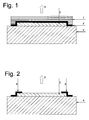
- the layers of the protective film laminate (a) preferably have a strip on at least one side of the layers. Again preferably, this strip is not bonded to an adhesive layer on the underlying layer of the protective film laminate (a).
- the strip allows easy and safe removal of a layer of the protective film laminate (a) by tearing.
- the adhesion of the lowermost layer of the protective film laminate (a) with that of the EL element (c) is stronger than the adhesion between the individual layers of the protective film laminate (a), respectively.
- the adhesion of the lowermost layer of the protective film laminate (a) with that of the EL element (c) may also be equal to the adhesion between the individual layers of the protective film laminate (a).
- the layers (ca), (cb) and (cc) are designed only in part with respect to the protective film laminate (a).
- Both the layers of the protective film laminate (a) and the adhesive layers including the adhesive layer (b) preferably have a refractive index at a temperature of 20 ° C in the range of 1.40 to 1.52, the difference in refractive indices between the layers of the Protective film laminate (a) and the adhesive layers including the adhesive layer (b) is not more than 0.2. In this way it is achieved that the intensity of the radiation of the EL element is not reduced.
- the layers of the protective film laminate (a) preferably have a thickness in the range from 0.01 to 0.3 mm, preferably in the range from 0.012 to 0.2 mm, particularly preferably in the range from 0.02 to 0.1 mm.
- Another object of the present invention is the use of an EL film composite as lighting on a motor vehicle.
- the position of the at least one EL film composite on the motor vehicle can be chosen arbitrarily.
- a motor vehicle is understood to mean that a motor vehicle is provided with the at least one EL film composite, so that the EL film composite attracts the observer and is recognized by the observer, that is to say to him in the eye, in particular when the EL foil composite lights up.
- the size of the at least one EL film composite on the motor vehicle can be chosen arbitrarily. Both parameters, that is, position and size, however, are preferably chosen so that the aforementioned object of the present invention is achieved, that is, the EL film composite is sufficiently large and positioned at that position of the motor vehicle, so that the motor vehicle Observer is noticeable and easily recognized by this.
- the individual EL film composites may have an identical or different design, that is, in particular size, shape and color.
- the individual EL foil composites can be attached to any position on the motor vehicle. In particular, it is possible for individual EL film composites to overlap.
- the at least one EL film composite can be attached in an appealing and / or striking external appearance in order to give the motor vehicle as a whole a pleasant and or eye-catching appearance.
- the EL film composite according to the invention is advantageously used everywhere where EL elements can and should be used, and where rapid cleaning of the EL element is desired.
- Another object of the present invention is therefore the use of an EL film composite as lighting on house walls, advertising columns, billboards, shop windows, walls of public transport stops, especially for advertising purposes, as Decoration lighting, as emergency lighting in the road, in the aerospace and military.
- the EL film composite has more than one EL element (c), which can emit light of the same or different color, and which can be electronically controlled separately, so that an animated luminous image can be achieved.
Landscapes
- Electroluminescent Light Sources (AREA)
Priority Applications (2)
| Application Number | Priority Date | Filing Date | Title |
|---|---|---|---|
| EP08020616A EP2221173A1 (fr) | 2008-11-27 | 2008-11-27 | Film composite électroluminescent doté d'un laminé à film protecteur |
| DE200920016123 DE202009016123U1 (de) | 2008-11-27 | 2009-11-26 | Elektrolumineszierender Folienverbund mit einem Schutzfolienlaminat |
Applications Claiming Priority (1)
| Application Number | Priority Date | Filing Date | Title |
|---|---|---|---|
| EP08020616A EP2221173A1 (fr) | 2008-11-27 | 2008-11-27 | Film composite électroluminescent doté d'un laminé à film protecteur |
Publications (1)
| Publication Number | Publication Date |
|---|---|
| EP2221173A1 true EP2221173A1 (fr) | 2010-08-25 |
Family
ID=40436265
Family Applications (1)
| Application Number | Title | Priority Date | Filing Date |
|---|---|---|---|
| EP08020616A Ceased EP2221173A1 (fr) | 2008-11-27 | 2008-11-27 | Film composite électroluminescent doté d'un laminé à film protecteur |
Country Status (2)
| Country | Link |
|---|---|
| EP (1) | EP2221173A1 (fr) |
| DE (1) | DE202009016123U1 (fr) |
Families Citing this family (2)
| Publication number | Priority date | Publication date | Assignee | Title |
|---|---|---|---|---|
| US10054298B2 (en) | 2013-12-16 | 2018-08-21 | Emdedesign Gmbh | Lamp or display comprising at least one light panel on a carrier plate |
| DE102016010345A1 (de) * | 2016-08-26 | 2018-03-01 | Robert Schmidt | selbstleuchtende geographische Gebrauchskarte |
Citations (9)
| Publication number | Priority date | Publication date | Assignee | Title |
|---|---|---|---|---|
| US4687968A (en) * | 1985-08-12 | 1987-08-18 | Rogers Corporation | Encapsulated electroluminescent lamp |
| US5592698A (en) | 1995-06-30 | 1997-01-14 | Woods; Marlen M. | Tear-off lens for transparent eye and face shield |
| WO2001034723A1 (fr) | 1999-11-10 | 2001-05-17 | Bundesdruckerei Gmbh | Phosphores electroluminescents a base de sulfure de zinc et leur procede de production |
| US6248261B1 (en) | 1998-08-26 | 2001-06-19 | Kabushiki Kaisha Toshiba | Electroluminescent phosphor and electroluminescent element using the same |
| US6388813B1 (en) | 1999-11-24 | 2002-05-14 | Bart Wilson | Optical stack of laminated removable lenses for face shields windows and displays |
| US20020109922A1 (en) | 1999-11-24 | 2002-08-15 | Bart Wilson | Optical stack of laminated removable lenses for face shields, windows, and displays |
| WO2006100164A1 (fr) | 2005-03-24 | 2006-09-28 | Schreiner Group Gmbh & Co. Kg | Element electroluminescent |
| US20070223211A1 (en) | 2006-03-23 | 2007-09-27 | John Jeffrey | Illumination device for a menu and method therefor |
| DE102006059203A1 (de) | 2006-12-13 | 2008-06-19 | Lyttron Technology Gmbh | Biegbares 3D-EL-HDFV Element und Herstellungsverfahren und Anwendung |
-
2008
- 2008-11-27 EP EP08020616A patent/EP2221173A1/fr not_active Ceased
-
2009
- 2009-11-26 DE DE200920016123 patent/DE202009016123U1/de not_active Expired - Lifetime
Patent Citations (11)
| Publication number | Priority date | Publication date | Assignee | Title |
|---|---|---|---|---|
| US4687968A (en) * | 1985-08-12 | 1987-08-18 | Rogers Corporation | Encapsulated electroluminescent lamp |
| US5592698A (en) | 1995-06-30 | 1997-01-14 | Woods; Marlen M. | Tear-off lens for transparent eye and face shield |
| US6248261B1 (en) | 1998-08-26 | 2001-06-19 | Kabushiki Kaisha Toshiba | Electroluminescent phosphor and electroluminescent element using the same |
| WO2001034723A1 (fr) | 1999-11-10 | 2001-05-17 | Bundesdruckerei Gmbh | Phosphores electroluminescents a base de sulfure de zinc et leur procede de production |
| US6388813B1 (en) | 1999-11-24 | 2002-05-14 | Bart Wilson | Optical stack of laminated removable lenses for face shields windows and displays |
| US20020109922A1 (en) | 1999-11-24 | 2002-08-15 | Bart Wilson | Optical stack of laminated removable lenses for face shields, windows, and displays |
| US6536045B1 (en) | 1999-11-24 | 2003-03-25 | Racing Optics | Tear-off optical stack having peripheral seal mount |
| US20030066118A1 (en) | 1999-11-24 | 2003-04-10 | Seth Wilson | Tear-off optical stack having peripheral seal mount |
| WO2006100164A1 (fr) | 2005-03-24 | 2006-09-28 | Schreiner Group Gmbh & Co. Kg | Element electroluminescent |
| US20070223211A1 (en) | 2006-03-23 | 2007-09-27 | John Jeffrey | Illumination device for a menu and method therefor |
| DE102006059203A1 (de) | 2006-12-13 | 2008-06-19 | Lyttron Technology Gmbh | Biegbares 3D-EL-HDFV Element und Herstellungsverfahren und Anwendung |
Also Published As
| Publication number | Publication date |
|---|---|
| DE202009016123U1 (de) | 2010-02-25 |
Similar Documents
| Publication | Publication Date | Title |
|---|---|---|
| US9035547B2 (en) | Marking having electroluminescent lighting effect, method for the production thereof | |
| WO2009000917A1 (fr) | Élément électroluminescent inorganique c.a. à couche épaisse présentant au moins deux alimentations, procédé de production et utilisation | |
| EP2191695A1 (fr) | Dispositif électroluminescent sur des matériaux textiles | |
| EP2103186A1 (fr) | Élément contenant un film métallique semi-transparent, procédé pour sa fabrication et utilisation de l'élément | |
| EP2158078A1 (fr) | Élément en verre composite, de préférence élément en verre composite de sécurité présentant une structure électroluminescente intégrée | |
| DE69710353T2 (de) | Elektrolumineszenter retroreflektierender gegenstand | |
| WO2008003621A1 (fr) | Élément el-hdvf 3d, procédé de fabrication et utilisation | |
| EP2215892A1 (fr) | Système d'électroluminescence ac à couche épaisse anorganique composé d'au moins une couche et comportant des couches conductrices de contours différents et en grande partie transparentes, procédé de fabrication et utilisation d'un tel système | |
| WO2008142012A1 (fr) | Vêtement de protection comprenant un laminé électroluminescent, son procédé de réalisation et son utilisation | |
| EP2334151A1 (fr) | Procédé de fabrication d'un élément électroluminescent par application de pulvérisation sur des objets formés d'une manière quelconque | |
| DE102009017669A1 (de) | Druckerzeugnis, umfassend mindestens ein Elektrolumineszenz-Element | |
| WO2008142010A2 (fr) | Tableau d'écriture présentant un élément électroluminescent, son procédé de réalisation et son utilisation | |
| EP2221173A1 (fr) | Film composite électroluminescent doté d'un laminé à film protecteur | |
| WO2008142013A1 (fr) | Élément électroluminescent comprenant des particules qui présentent des nanostructures | |
| WO2008071412A1 (fr) | Élément el tridimensionnel à déformation à haute pression flexible, son procédé de fabrication et son utilisation | |
| EP1863674B1 (fr) | Plaque pour realiser un panneau electroluminescent | |
| WO2012004295A1 (fr) | Document de sécurité et/ou de valeur contenant un ensemble électroluminescent | |
| HK1144519A (en) | Inorganic thick film ac electroluminescence element having at least two inputs, and production method and use | |
| WO2006050954A1 (fr) | Vetement protecteur reflechissant |
Legal Events
| Date | Code | Title | Description |
|---|---|---|---|
| PUAI | Public reference made under article 153(3) epc to a published international application that has entered the european phase |
Free format text: ORIGINAL CODE: 0009012 |
|
| AK | Designated contracting states |
Kind code of ref document: A1 Designated state(s): AT BE BG CH CY CZ DE DK EE ES FI FR GB GR HR HU IE IS IT LI LT LU LV MC MT NL NO PL PT RO SE SI SK TR |
|
| AX | Request for extension of the european patent |
Extension state: AL BA MK RS |
|
| STAA | Information on the status of an ep patent application or granted ep patent |
Free format text: STATUS: THE APPLICATION HAS BEEN REFUSED |
|
| 18R | Application refused |
Effective date: 20101008 |