EP2226699A2 - Appareil et procédé d'alimentation électrique d'un dispositif électronique - Google Patents
Appareil et procédé d'alimentation électrique d'un dispositif électronique Download PDFInfo
- Publication number
- EP2226699A2 EP2226699A2 EP09161396A EP09161396A EP2226699A2 EP 2226699 A2 EP2226699 A2 EP 2226699A2 EP 09161396 A EP09161396 A EP 09161396A EP 09161396 A EP09161396 A EP 09161396A EP 2226699 A2 EP2226699 A2 EP 2226699A2
- Authority
- EP
- European Patent Office
- Prior art keywords
- power
- ldo
- converter
- input
- controller
- Prior art date
- Legal status (The legal status is an assumption and is not a legal conclusion. Google has not performed a legal analysis and makes no representation as to the accuracy of the status listed.)
- Granted
Links
Images


Classifications
-
- H—ELECTRICITY
- H02—GENERATION; CONVERSION OR DISTRIBUTION OF ELECTRIC POWER
- H02M—APPARATUS FOR CONVERSION BETWEEN AC AND AC, BETWEEN AC AND DC, OR BETWEEN DC AND DC, AND FOR USE WITH MAINS OR SIMILAR POWER SUPPLY SYSTEMS; CONVERSION OF DC OR AC INPUT POWER INTO SURGE OUTPUT POWER; CONTROL OR REGULATION THEREOF
- H02M1/00—Details of apparatus for conversion
- H02M1/36—Means for starting or stopping converters
-
- G—PHYSICS
- G05—CONTROLLING; REGULATING
- G05F—SYSTEMS FOR REGULATING ELECTRIC OR MAGNETIC VARIABLES
- G05F1/00—Automatic systems in which deviations of an electric quantity from one or more predetermined values are detected at the output of the system and fed back to a device within the system to restore the detected quantity to its predetermined value or values, i.e. retroactive systems
- G05F1/10—Regulating voltage or current
- G05F1/46—Regulating voltage or current wherein the variable actually regulated by the final control device is DC
-
- H—ELECTRICITY
- H02—GENERATION; CONVERSION OR DISTRIBUTION OF ELECTRIC POWER
- H02M—APPARATUS FOR CONVERSION BETWEEN AC AND AC, BETWEEN AC AND DC, OR BETWEEN DC AND DC, AND FOR USE WITH MAINS OR SIMILAR POWER SUPPLY SYSTEMS; CONVERSION OF DC OR AC INPUT POWER INTO SURGE OUTPUT POWER; CONTROL OR REGULATION THEREOF
- H02M3/00—Conversion of DC power input into DC power output
- H02M3/22—Conversion of DC power input into DC power output with intermediate conversion into AC
- H02M3/24—Conversion of DC power input into DC power output with intermediate conversion into AC by static converters
- H02M3/28—Conversion of DC power input into DC power output with intermediate conversion into AC by static converters using discharge tubes with control electrode or semiconductor devices with control electrode to produce the intermediate AC
Definitions
- This document relates to an apparatus and method of supplying power to an electronic device.
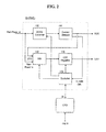
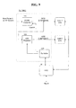
- power supplies for electronic devices such as mobile phones, personal digital assistants (PDAs), and laptop computers include a power management integrated circuit (PMIC) 10 as shown in Fig. 1 .
- PMIC power management integrated circuit
- the PMIC 10 includes a controller 100, a plurality of DC/DC converters 110 1 , 110 2 , and 110 3 , and a plurality of low-dropout (LDO) regulators 120 1 , 120 2 , and 120 3 .
- LDO low-dropout
- the controller 100 enables the plurality of DC/DC converters and LDO regulators to have a predetermined initial (power) value when the electronic device is system-booted.
- main power supplied to the PMIC 10 is converted to different output power components.
- main power of 3.7V/1500mA supplied from a battery is converted to DCO1 (DC output1) power of 2.5V/450mA by the first DC/DC converter 110 1 .
- the main power is also converted to DCO2 power of 3.3V/1000mA by the second DC/DC converter 110 2 , and to DCO3 power of 1.3V/500mA by the third DC/DC converter 110 3 .
- the main power of 3.7V/1500mA is converted to LDO1 power of 1.8V/100mA by the first LDO regulator 120 1 , LDO2 power of 1.5V/200mA by the second LDO regulator 120 2 , and LDO3 power of 1.2V/150mA by the third LDO regulator 120 3 .
- the DC/DC converter is a voltage converting device for making an output voltage higher or lower than an input voltage.
- a converter for converting a low input voltage to a higher output voltage is called “step-up converter” and a converter for converting a high input voltage to a lower output voltage is called “step-down converter”.
- a step-up converter employs a buck DC/DC converter and a step-down converter employs a boost converter.
- DC/DC converters are classified into PWM (Pulse Width Modulation) type DC/DC converters and PFM (Pulse Frequency Modulation) type DC/DC converters based on switching scheme.
- LDO regulators have the advantage of being capable of supplying a stable voltage having reduced ripple components, as is widely known. In the case of a high input voltage, however, significant power loss may occur while the high input voltage is converted to a lower output voltage.
- An aspect of this document provides an apparatus and method of supplying power to an electronic device, which may reduce power loss caused by LDO regulators in a power management integrated circuit (PMIC).
- PMIC power management integrated circuit
- an apparatus for supplying power to an electronic device includes a plurality of DC/DC converters configure to respectively output power; a plurality of low-dropout (LDO) regulators configured to respectively output converted power to power-consuming loads; one or more switching elements that select any one of a plurality of different powers including the output power of the DC/DC converters and input the selected power to the plurality of LDO regulators; and a controller that controls operation of the one or more switching elements based on the converted power and the power-consuming loads.
- LDO low-dropout
- an apparatus for supplying power to an electronic device includes a plurality of DC/DC converters configured to output power; a plurality of LDO regulators configured to output converted power; and a controller configured to control supply of the output power of the at least one of the plurality of DC/DC converters to the at least one of the plurality of LDO regulators as input power, and to variably control the at least one of the plurality of DC/DC converters to variably adjust the input power of the at least one of the plurality of LDO regulators.
- a method for supplying power to an electronic device includes selecting either one of main power supplied from a battery and DC Out (DCO) power supplied from a DC/DC converter to supply the selected power to at least one LDO regulator as input power; and changing the selected power supplied to the at least one LDO regulator to the other based on a state of a power-consuming load that is connected at an output end of the at least one LDO regulator.
- DCO DC Out
- a method for supplying power to an electronic device includes supplying output power of a DC/DC converter to an LDO regulator as input power; and variably controlling the DC/DC converter based on a state of a load connected at an output end of the DC/DC converter and a state of a load connected at an output end of the LDO regulator to change the input power of the LDO regulator.
- Fig. 1 is a view illustrating a construction of a conventional power supply.
- Fig. 2 is a view schematically illustrating a construction of a power supply according to an embodiment.
- Figs. 3 to 8 are views illustrating power supplies according to embodiments in more detail.
- Figs. 9 and 10 are views schematically illustrating power supplies according to other embodiments.
- Fig. 11 is a flowchart illustrating a power supplying method according to an embodiment.
- the power supply employs a power management integrated circuit (PMIC) that includes a plurality of DC/DC converters, a plurality of LDO regulators, and a controller.
- PMIC power management integrated circuit
- the PMIC includes a switching element for selecting any one of a plurality of different powers sources and supplies as low an input voltage as possible to the LDO regulator.
- a switching element 140 may be supplied with main power from a battery and DCO power converted by a DC/DC converter 110, as shown in Fig. 2 .
- a controller 100 controls a switching element 140 to selectively supply the main power or the DCO power to an LDO regulator 120.
- a current detector 130 may be provided at the rear end of the DC/DC converter 110, as shown in Fig. 2 .
- the controller 100 controls the switching element 140 so that a current value detected by the current detector 130 does not exceed a predetermined reference current value.
- the controller 100 controls the switching element 140 to selectively supply the LDO regulator 120 with the main power having relatively high voltage and current values.
- the controller 100 controls the switching element 140 to selectively supply the LDO regulator 120 with the DCO power having relatively low voltage and current values.
- the input voltage of the power supplied to the LDO regulator 120 may become as low as possible, and this may reduce power loss caused by the LDO regulator 120.
- the controller 100 predicts whether the number of loads connected at the rear end of the DC/DC converter 110 and the LDO regulator 120 increases or decreases by interfacing with a CPU 20 that executes various application programs in response to a user's key entries (Key In).
- the controller 100 selects the main power and supplies it to the LDO regulator 120, and when the number of loads is predicted to decrease, the controller 100 selects the DCO power and supplies it to the LDO regulator 120.
- the input voltage supplied to the LDO regulator 120 may be as low as possible, and thus, power loss caused by the LDO regulator 120 may be reduced.
- the controller 100 determines whether the source of supplying the main power is a battery, or an external power source that supplies unlimited power, and if the source is an external power source, the controller 100 allows the external power source to continue to supply power to the LDO regulator 120.
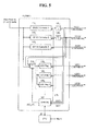
- Fig. 3 is a view illustrating a power supply for an electronic device according to an embodiment in more detail.
- a power management integrated circuit 10 includes a controller 100, a plurality of DC/DC converters 110 1 , 110 2 , and 110 3 , and a plurality of LDO regulators 120 1 , 120 2 , and 120 3 .
- Switching elements 140 1 , 140 2 , and 140 3 are provided at a front (input) ends of the LDO regulators to select different power.
- At least one current detector may be provided at the rear end of at least one of the DC/DC converters.
- a first current detector 130 1 and a second current detector 130 2 may be provided at the rear ends of the first DC/DC converter 110 1 and the second DC/DC converter 110 2 , respectively, and the first to third switching elements 140 1 to 140 3 may be provided at the front ends of the first to third LDO regulators 120 1 to 120 3 , respectively.
- the first to third switching elements 140 1 to 140 3 are supplied with the main power of 3.7V/1500mA, the DCO1 power of 2.5V/450mA, and the DCO2 power of 3.3V/1000mA, respectively.
- the power supplied to the first to third switching elements 140 1 to 140 3 has higher voltage than the output voltages of the first to third LDO regulators 120 1 to 120 3 .
- the DCO3 power of 1.3V/500mA converted by the third DC/DC converter 110 3 is not appropriate as the input power of the first LDO regulator 120 1 that outputs the LDO1 power of 1.8V1100mA, or as the input power of the second LDO regulator 120 2 that outputs the LDO2 power of 1.5V/200mA.
- the DCO3 power is not used as the input power of the first to third switching elements 140 1 to 140 3 .
- the controller 100 verifies the current value detected by the first current detector 130 1 connected to the DCO1 power source and supplies the selected DCO1 power of 2.5V/450mA to the first LDO regulator 120 1 as the input power, as shown in Fig. 4 .
- the controller 100 determines that the number of power-consuming loads connected at the rear end of the first DC/DC converter 1101 and at the rear end of the first LDO regulator 1201 has increased.
- a reference current value e.g. 400mA
- the controller 100 selects the DCO2 power of 3.3V/1000mA among the plurality of power sources input to the first switching element 140 1 and supplies it to the first LDO regulator 120 1 as the input power.
- the controller 100 verifies the current value detected by the second current detector 130 2 connected to the DCO2 power source.
- a reference current value e.g. 900mA
- the controller 100 determines that the number of power-consuming loads connected at the rear end of the second DC/DC converter 110 2 and at the rear end of the first LDO regulator 120 1 has increased.
- the controller 100 When the current value detected by the second current detector 130 2 exceeds the reference current value set to be lower than, for example, the DCO2 power of 3.3V/1000mA by the constant current value, the controller 100 performs a switching control operation of selecting the main power of 3.7V/1500mA among the plurality of power input to the first switching element 140 1 and supplying it to the first LDO regulator 120 1 as the input power.
- the controller 100 verifies the current values detected by the first current detector 130 1 and the second current detector 130 2 , preferentially selects power having as low a voltage as possible, and supplies it to the LDO regulator as the input power. This enables power loss caused by the LDO regulator to be minimized.
- the controller 100 selects the DCO1 power of 2.5V/450mA having the lowest voltage value and supplies it to the first LDO regulator 120 1 as the input power.
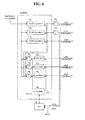
- the switching element may be commonly connected to the front ends of the plurality of LDO regulators.
- the first switching element 140 1 may be commonly connected to the front ends of the LDO regulators 120 1 to 120 3 as shown in Fig. 5 .
- first current detector 130 1 and the second current detector 130 2 may be provided outside the PMIC 10 as shown in Fig. 6 .
- the current values detected by the current detectors may be input to the controller 100 via the CPU 20.
- the switching element may be commonly connected to the front ends of the plurality of LDO regulators as shown in Fig. 7 .
- the CPU 20 executes various application programs in response to a user's key entries. For example, upon receipt of a request to operate a camera module connected to the rear end of the first DC/DC converter 110 1 , the CPU 20 generates a control signal and transmits it to the controller 100 so that the controller 100 may execute a corresponding application program.
- the controller 100 Upon receipt of the control signal, the controller 100 predicts that the number of loads provided at the rear end of the first DC/DC converter 110 1 will increase, and controls the first switching element 140 1 to change the input power supplied to the first LDO regulator 120 1 to power having higher voltage and current values than the present input power in advance.
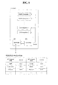
- the PMIC 10 may include a non-volatile memory such as EEPROM which stores and manages control values of power sequences for controlling the order and timing of ON/OFF switching of the plurality of DC/DC converters and the plurality of LDO regulators.
- EEPROM non-volatile memory
- the non-volatile memory stores and manages as a DCO/LDO control database the control values of power sequences for supplying power suitably for processor unit A and processor unit B manufactured by different makers.
- Processor unit A which is a communication processor, may be manufactured by makers such as EMP, Qualcomm, Infineon, etc., and the DCO/LDO control database stores and manages the control values of power sequences suitably for processor unit A of each maker.
- Processor unit B which is a digital signal processor, may be manufactured by makers such as nVidia, QMAP, Marvell, etc., and the DCO/LDO control database stores and manages the control values of power sequences suitably for processor unit B of each maker.
- engineers may design the PMIC more easily by identifying the makers of processor unit A and processor unit B, selecting and designating corresponding DCO/LDO control values from the DCO/LDO control database, and executing power sequences corresponding to the DCO/LDO control values.
- output voltage from the DC/DC converter included in the PMIC may be supplied to the LDO regulator as the input power without separate switching elements.
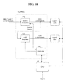
- the controller 100 interfaces with the CPU 20 to determine whether a power-consuming load 1 connected to the DC/DC converter 110 is operating, as shown in Fig. 9 .
- the load 1 is a block that performs a specific function, such as an LCD module, a wired LAN module, a wireless LAN module, a Bluetooth module, a camera module, a projector module, etc.
- the controller 100 variably controls the DC/DC converter 110 so that the output power DCO has voltage and current values lower than 2.5V/450mA, for example, 2.0V/300mA.
- the controller 100 when the controller 100 interfaces with the CPU 20 and determines that the load 1 connected to the DC/DC converter 110 is operating, the controller 100 variably controls the DC/DC converter 110 to return the output power DCO to the original voltage and current values, 2.5V/450mA, so that normal operating power is supplied to the load 1 connected to the DC/DC converter 110.
- a high-power load such as a camera module is connected to the rear end of the DC/DC converter 110
- a low-power load such as a memory module is connected to the rear end of the LDO regulator 120
- the CPU 20 selectively turns the camera module and the memory module on/off in response to the user's key entries.
- Fig. 11 is a flowchart illustrating a power supplying method according to an embodiment. The method will now be described with reference to Fig. 6 .
- step S10 the controller 100 included in the PMIC 10 determines whether the DCO1 power may be selected as the input power of the LDO regulator.
- the controller 100 controls the switching element to selectively supply the DCO1 power to the LDO regulator as the input power (step S12), and then identifies the current value detected by the current detector or interfaces with the CPU to determine whether there is any load using the DCO1 power.
- the controller 100 variably controls the first DC/DC converter that outputs the DCO1 power to turn down the DCO1 power (step S14).
- the turned-down DCO1 power should be adjusted to have a higher voltage than the LDO output voltage.
- step S15 the controller 100 repeatedly performs the above series of steps.
- the controller 100 determines whether the DCO2 power may be selected as the input power of the LDO regulator.
- the controller 100 controls the switching element to selectively supply the DCO2 power to the LDO regulator as the input power (step S17), and identifies the current value detected by the current detector, or interfaces with the CPU to determine whether there is any load using the DCO2 power.
- the controller 100 variably controls the second DC/DC converter that outputs the DCO2 power to turn down the DCO2 power (step S19).
- the turned-down DCO2 power should be adjusted to have a higher voltage than the LDO output voltage.
- step S20 When the number of loads using the DCO2 power increases (step S20), the controller 100 repeatedly performs the above series of steps. If the main power source is not the battery but an external power source supplying unlimited power, the controller 100 continues to supply power to the LDO regulator as the input power by using the external power source (step S21).
Landscapes
- Engineering & Computer Science (AREA)
- Physics & Mathematics (AREA)
- Electromagnetism (AREA)
- General Physics & Mathematics (AREA)
- Radar, Positioning & Navigation (AREA)
- Automation & Control Theory (AREA)
- Power Engineering (AREA)
- Dc-Dc Converters (AREA)
- Charge And Discharge Circuits For Batteries Or The Like (AREA)
- Direct Current Feeding And Distribution (AREA)
Applications Claiming Priority (1)
| Application Number | Priority Date | Filing Date | Title |
|---|---|---|---|
| KR1020090017501A KR101552165B1 (ko) | 2009-03-02 | 2009-03-02 | 전자 기기의 전원 공급 장치 및 방법 |
Publications (3)
| Publication Number | Publication Date |
|---|---|
| EP2226699A2 true EP2226699A2 (fr) | 2010-09-08 |
| EP2226699A3 EP2226699A3 (fr) | 2014-12-03 |
| EP2226699B1 EP2226699B1 (fr) | 2017-12-06 |
Family
ID=42235382
Family Applications (1)
| Application Number | Title | Priority Date | Filing Date |
|---|---|---|---|
| EP09161396.8A Active EP2226699B1 (fr) | 2009-03-02 | 2009-05-28 | Appareil et procédé d'alimentation électrique d'un dispositif électronique |
Country Status (3)
| Country | Link |
|---|---|
| US (1) | US8026636B2 (fr) |
| EP (1) | EP2226699B1 (fr) |
| KR (1) | KR101552165B1 (fr) |
Cited By (6)
| Publication number | Priority date | Publication date | Assignee | Title |
|---|---|---|---|---|
| CN103499990A (zh) * | 2012-10-11 | 2014-01-08 | 成都芯源系统有限公司 | 一种稳压器、数字校正稳压器的系统及方法 |
| US8988054B2 (en) | 2011-12-27 | 2015-03-24 | St-Ericsson Sa | Single feedback loop for parallel architecture buck converter—LDO regulator |
| EP2619843A4 (fr) * | 2010-09-20 | 2017-01-25 | Nokia Technologies Oy | Fourniture d'un courant à un composant |
| WO2020039105A1 (fr) * | 2018-08-23 | 2020-02-27 | Erle Robotics, S.L. | Module de gestion de puissance pour des robots et procédé de gestion de puissance qui fait appel à ce dernier |
| WO2020231014A1 (fr) | 2019-05-16 | 2020-11-19 | Samsung Electronics Co., Ltd. | Dispositif électronique de gestion d'énergie et son procédé de fonctionnement |
| EP3928179A4 (fr) * | 2019-05-16 | 2022-05-18 | Samsung Electronics Co., Ltd. | Dispositif électronique de gestion d'énergie et son procédé de fonctionnement |
Families Citing this family (49)
| Publication number | Priority date | Publication date | Assignee | Title |
|---|---|---|---|---|
| US8324756B2 (en) * | 2008-10-06 | 2012-12-04 | Texas Instruments Incorporated | Automatic on-chip detection of power supply configuration-modes for integrated chips |
| JP5494177B2 (ja) * | 2010-04-21 | 2014-05-14 | 富士通株式会社 | 半導体装置 |
| KR101052284B1 (ko) * | 2010-10-25 | 2011-07-27 | 엘아이지넥스원 주식회사 | 파워 시퀀스/클록 타이밍 제어 장치 |
| US9570908B2 (en) * | 2012-02-09 | 2017-02-14 | Silicon Laboratories Inc. | Power management system |
| KR101923585B1 (ko) * | 2012-07-11 | 2018-11-30 | 삼성전자 주식회사 | 휴대단말기의 전원공급장치 및 방법 |
| US20140265563A1 (en) * | 2013-03-15 | 2014-09-18 | Henry W. Schrader | Hierarchical power conditioning and distribution array |
| US9673699B1 (en) * | 2013-08-08 | 2017-06-06 | Iml International | Floating charge pump voltage converter |
| US20150214770A1 (en) * | 2014-01-29 | 2015-07-30 | Mediatek Inc. | System and method supporting hybrid power/battery scheme |
| US9806707B2 (en) | 2014-02-07 | 2017-10-31 | Qualcomm Incorporated | Power distribution network (PDN) conditioner |
| US10044268B1 (en) * | 2014-06-04 | 2018-08-07 | Empower Semiconductor, Inc. | Devices and techniques for controlling voltage regulation |
| EP2952914A1 (fr) | 2014-06-06 | 2015-12-09 | Dialog Semiconductor GmbH | Circuit de surveillance de courant de sortie |
| US9645598B2 (en) * | 2014-07-14 | 2017-05-09 | Lenovo Enterprise Solutions (Singapore) Pte. Ltd. | Controlling distributed power stages responsive to the activity level of functions in an integrated circuit |
| US9784791B2 (en) | 2014-07-18 | 2017-10-10 | Intel Corporation | Apparatus and method to debug a voltage regulator |
| US9568926B2 (en) * | 2014-09-29 | 2017-02-14 | Nxp B.V. | Power supply interface having multiple voltage sources |
| KR102244992B1 (ko) * | 2014-10-17 | 2021-04-28 | 삼성전자주식회사 | 부하 전류 정보를 제공하는 전력관리 집적회로 및 그것을 포함하는 전자 장치 |
| US9785222B2 (en) | 2014-12-22 | 2017-10-10 | Qualcomm Incorporated | Hybrid parallel regulator and power supply combination for improved efficiency and droop response with direct current driven output stage attached directly to the load |
| US9891646B2 (en) | 2015-01-27 | 2018-02-13 | Qualcomm Incorporated | Capacitively-coupled hybrid parallel power supply |
| KR102345396B1 (ko) | 2015-04-03 | 2021-12-31 | 삼성디스플레이 주식회사 | 전원 관리 드라이버 및 이를 포함하는 표시 장치 |
| US9923457B2 (en) * | 2015-04-23 | 2018-03-20 | Taiwan Semiconductor Manufacturing Company, Ltd. | Regulated power converter and method of operating the same |
| US9983643B2 (en) * | 2015-09-01 | 2018-05-29 | Silicon Laboratories Inc. | Providing multiple power paths in an integrated circuit |
| US9819189B2 (en) | 2015-09-02 | 2017-11-14 | Qualcomm Incorporated | Area and power efficient switchable supply network for powering multiple digital islands |
| CN106959844A (zh) | 2016-01-12 | 2017-07-18 | 西安中兴新软件有限责任公司 | 一种低电开机处理的方法及装置 |
| US9898020B2 (en) | 2016-03-02 | 2018-02-20 | Qualcomm Incorporated | Power supply voltage priority based auto de-rating for power concurrency management |
| KR102695929B1 (ko) | 2016-07-27 | 2024-08-16 | 삼성전자주식회사 | 전력 관리 장치 및 이를 포함하는 전자 장치 |
| KR102695310B1 (ko) * | 2016-08-09 | 2024-08-13 | 삼성전자주식회사 | 전원 관리 집적 회로를 포함하는 전자 장치 |
| JP6774267B2 (ja) * | 2016-08-25 | 2020-10-21 | 矢崎総業株式会社 | 電圧変換装置 |
| US20180061984A1 (en) | 2016-08-29 | 2018-03-01 | Macom Technology Solutions Holdings, Inc. | Self-biasing and self-sequencing of depletion-mode transistors |
| US20180145682A1 (en) * | 2016-11-18 | 2018-05-24 | Macom Technology Solutions Holdings, Inc. | Positive and negative dc-dc converter for biasing rf circuits |
| US10110218B2 (en) | 2016-11-18 | 2018-10-23 | Macom Technology Solutions Holdings, Inc. | Integrated biasing for pin diode drivers |
| US10560062B2 (en) * | 2016-11-18 | 2020-02-11 | Macom Technology Solutions Holdings, Inc. | Programmable biasing for pin diode drivers |
| US20180358886A1 (en) | 2017-06-09 | 2018-12-13 | MACOM Technology Solution Holdings, Inc. | Integrated solution for multi-voltage generation with thermal protection |
| US10579087B2 (en) * | 2018-05-02 | 2020-03-03 | Silicon Laboratories Inc. | System, apparatus and method for flexible control of a voltage regulator of an integrated circuit |
| KR102110656B1 (ko) | 2018-06-21 | 2020-05-14 | 주식회사 유니네트워크 | 마이닝 시스템을 위한 컴퓨터용 전원 공급 장치 및 그의 전원 공급 방법 |
| KR102545301B1 (ko) | 2018-09-10 | 2023-06-16 | 삼성전자주식회사 | 반도체 회로 |
| US11429173B2 (en) * | 2018-12-21 | 2022-08-30 | Intel Corporation | Apparatus and method for proactive power management to avoid unintentional processor shutdown |
| WO2020166877A1 (fr) * | 2019-02-12 | 2020-08-20 | 주식회사 실리콘마이터스 | Appareil de gestion d'énergie utilisable dans une batterie possédant une pluralité de cellules connectées en série |
| KR102699041B1 (ko) | 2019-03-29 | 2024-08-26 | 삼성전자주식회사 | 복수의 ldo 레귤레이터들을 포함하는 레귤레이팅 회로 및 이의 동작 방법 |
| CN111934565B (zh) * | 2019-05-13 | 2021-11-23 | 鸿富锦精密电子(天津)有限公司 | 电源装置 |
| KR102801376B1 (ko) * | 2019-05-16 | 2025-05-02 | 삼성전자주식회사 | 전력 관리를 수행하는 전자 장치 및 그 동작 방법 |
| KR102801403B1 (ko) * | 2019-11-18 | 2025-04-30 | 삼성전자주식회사 | 전력 관리를 수행하는 전자 장치 및 그 동작 방법 |
| US11709512B2 (en) * | 2021-09-14 | 2023-07-25 | Apple Inc. | System-on-chip with power supply mode having reduced number of phases |
| DE112022003384B4 (de) * | 2021-09-14 | 2024-12-12 | Apple Inc. | System-On-Chip mit Leistungsversorgungsmodus mit reduzierter Anzahl von Phasen |
| CN116131615A (zh) * | 2021-11-12 | 2023-05-16 | 瑞昱半导体股份有限公司 | 供电管理装置与供电管理方法 |
| US12093068B2 (en) * | 2022-06-14 | 2024-09-17 | Apple Inc. | Scalable low dropout regulator having multiple pass circuits |
| KR20240003636A (ko) | 2022-07-01 | 2024-01-09 | 에스케이하이닉스 주식회사 | 전압 제공 회로 |
| CN116054307B (zh) * | 2022-07-27 | 2023-10-20 | 荣耀终端有限公司 | 电源控制系统及电子设备 |
| KR102844371B1 (ko) * | 2023-06-07 | 2025-08-08 | 한국알프스 주식회사 | 다중 스위치 신호의 단일 핀 입력에 의한 웨이크업 기능을 갖는 디바이스 |
| US12483111B2 (en) * | 2023-11-09 | 2025-11-25 | Mediatek Inc. | Voltage control method and electronic system |
| US20260064174A1 (en) * | 2024-08-30 | 2026-03-05 | Super Micro Computer, Inc. | Power Supply Units in Server Computers |
Family Cites Families (8)
| Publication number | Priority date | Publication date | Assignee | Title |
|---|---|---|---|---|
| JPH1141825A (ja) * | 1997-07-14 | 1999-02-12 | Victor Co Of Japan Ltd | 電源切替装置 |
| JP2000032753A (ja) | 1998-07-14 | 2000-01-28 | Yamaha Corp | 直流安定化電源装置 |
| US6801027B2 (en) * | 2002-09-26 | 2004-10-05 | Itt Manufacturing Enterprises, Inc. | Power conversion in variable load applications |
| KR100480067B1 (ko) * | 2002-10-15 | 2005-03-31 | 엘지전자 주식회사 | 휴대용 단말기의 전류 절감 장치 |
| US7084612B2 (en) | 2004-04-30 | 2006-08-01 | Micrel, Inc. | High efficiency linear regulator |
| JP2007244046A (ja) | 2006-03-06 | 2007-09-20 | Sharp Corp | 電源回路 |
| KR101134696B1 (ko) * | 2007-01-12 | 2012-04-09 | 엘지전자 주식회사 | 휴대단말기의 전원관리장치 및 그 방법 |
| US20100060078A1 (en) * | 2008-09-08 | 2010-03-11 | Micrel, Incorporated | Dual Input LDO Regulator With Controlled Transition Between Power Supplies |
-
2009
- 2009-03-02 KR KR1020090017501A patent/KR101552165B1/ko active Active
- 2009-05-15 US US12/466,612 patent/US8026636B2/en active Active
- 2009-05-28 EP EP09161396.8A patent/EP2226699B1/fr active Active
Cited By (10)
| Publication number | Priority date | Publication date | Assignee | Title |
|---|---|---|---|---|
| EP2619843A4 (fr) * | 2010-09-20 | 2017-01-25 | Nokia Technologies Oy | Fourniture d'un courant à un composant |
| US8988054B2 (en) | 2011-12-27 | 2015-03-24 | St-Ericsson Sa | Single feedback loop for parallel architecture buck converter—LDO regulator |
| CN103499990A (zh) * | 2012-10-11 | 2014-01-08 | 成都芯源系统有限公司 | 一种稳压器、数字校正稳压器的系统及方法 |
| CN103499990B (zh) * | 2012-10-11 | 2016-01-13 | 成都芯源系统有限公司 | 一种稳压器、数字校正稳压器的系统及方法 |
| WO2020039105A1 (fr) * | 2018-08-23 | 2020-02-27 | Erle Robotics, S.L. | Module de gestion de puissance pour des robots et procédé de gestion de puissance qui fait appel à ce dernier |
| WO2020231014A1 (fr) | 2019-05-16 | 2020-11-19 | Samsung Electronics Co., Ltd. | Dispositif électronique de gestion d'énergie et son procédé de fonctionnement |
| EP3928179A4 (fr) * | 2019-05-16 | 2022-05-18 | Samsung Electronics Co., Ltd. | Dispositif électronique de gestion d'énergie et son procédé de fonctionnement |
| US11379025B2 (en) | 2019-05-16 | 2022-07-05 | Samsung Electronics Co., Ltd. | Electronic device for performing power management and method for operating the same |
| US12204390B2 (en) | 2019-05-16 | 2025-01-21 | Samsung Electronics Co., Ltd. | Electronic device for performing power management and method for operating the same |
| EP4496202A3 (fr) * | 2019-05-16 | 2025-04-02 | Samsung Electronics Co., Ltd. | Dispositif électronique pour effectuer une gestion d'énergie et son procédé de fonctionnement |
Also Published As
| Publication number | Publication date |
|---|---|
| US20100219687A1 (en) | 2010-09-02 |
| EP2226699A3 (fr) | 2014-12-03 |
| KR20100098826A (ko) | 2010-09-10 |
| KR101552165B1 (ko) | 2015-09-18 |
| US8026636B2 (en) | 2011-09-27 |
| EP2226699B1 (fr) | 2017-12-06 |
Similar Documents
| Publication | Publication Date | Title |
|---|---|---|
| EP2226699B1 (fr) | Appareil et procédé d'alimentation électrique d'un dispositif électronique | |
| EP2685635B1 (fr) | Appareil et procédé permettant d'alimenter un terminal mobile utilisant des convertisseurs de type buck-boost | |
| US11061423B2 (en) | Power management device and electronic device including the same | |
| EP3071980B1 (fr) | Circuits de réglage de tension dynamique et procédés associés | |
| JP5167645B2 (ja) | 電子機器および直流電圧変換システム | |
| EP2495633B1 (fr) | Procédé et appareil de régulateur de commutation de courant à faible veille | |
| JP6262478B2 (ja) | 電源回路およびその制御回路、電子機器 | |
| JP4553879B2 (ja) | 電子機器 | |
| US9705393B2 (en) | Voltage regulator | |
| EP2538515A1 (fr) | Régulateur de tension à courant limité à entrées multiples et procédé correspondant | |
| US20130335058A1 (en) | Adjusting Voltage Regulator Operating Parameters | |
| US20150280493A1 (en) | Method for controlling power supply and electronic device | |
| US20130162237A1 (en) | Energy-based Oriented Switching Mode Power Supply | |
| KR102838810B1 (ko) | 전력 회로 및 전력 회로의 동작 방법 | |
| CN103885392A (zh) | 供电系统、电压调节装置及其控制方法 | |
| EP2775601B1 (fr) | Adaption des domaines de mode d'opération des alimentations à découpages par les seuils programmables | |
| KR101663228B1 (ko) | 전원 관리 방법 및 장치 | |
| US20250132560A1 (en) | Battery hot swapping | |
| EP2405318A1 (fr) | Circuit d'alimentation électrique | |
| WO2017157113A1 (fr) | Régulateur continu-continu et son procédé de commande de démarrage en douceur, et dispositif de commande | |
| KR102428555B1 (ko) | 전자 기기의 고속 웨이크-업을 위한 직류-직류 변환 장치 및 그 동작 방법 | |
| CN117413237A (zh) | 用于联动电压调节器的负载均衡架构 | |
| TWI914384B (zh) | 無縫式非線性電壓調節控制至線性控制之設備及方法 | |
| JP2008166076A (ja) | 電子機器システム、および電源制御方法 | |
| CN119543637A (zh) | 电荷泵转换模块、电源管理电路及方法、供电模组 |
Legal Events
| Date | Code | Title | Description |
|---|---|---|---|
| PUAI | Public reference made under article 153(3) epc to a published international application that has entered the european phase |
Free format text: ORIGINAL CODE: 0009012 |
|
| 17P | Request for examination filed |
Effective date: 20090528 |
|
| AK | Designated contracting states |
Kind code of ref document: A2 Designated state(s): AT BE BG CH CY CZ DE DK EE ES FI FR GB GR HR HU IE IS IT LI LT LU LV MC MK MT NL NO PL PT RO SE SI SK TR |
|
| RIC1 | Information provided on ipc code assigned before grant |
Ipc: G05F 1/46 20060101AFI20140630BHEP Ipc: H02M 3/00 20060101ALI20140630BHEP Ipc: H02J 1/00 20060101ALI20140630BHEP |
|
| PUAL | Search report despatched |
Free format text: ORIGINAL CODE: 0009013 |
|
| AK | Designated contracting states |
Kind code of ref document: A3 Designated state(s): AT BE BG CH CY CZ DE DK EE ES FI FR GB GR HR HU IE IS IT LI LT LU LV MC MK MT NL NO PL PT RO SE SI SK TR |
|
| RIC1 | Information provided on ipc code assigned before grant |
Ipc: H02M 3/00 20060101ALI20141028BHEP Ipc: G05F 1/46 20060101AFI20141028BHEP Ipc: H02J 1/00 20060101ALI20141028BHEP |
|
| RBV | Designated contracting states (corrected) |
Designated state(s): AT BE BG CH CY CZ DE DK EE ES FI FR GB GR HR HU IE IS IT LI LT LU LV MC MK MT NL NO PL PT RO SE SI SK TR |
|
| GRAP | Despatch of communication of intention to grant a patent |
Free format text: ORIGINAL CODE: EPIDOSNIGR1 |
|
| STAA | Information on the status of an ep patent application or granted ep patent |
Free format text: STATUS: GRANT OF PATENT IS INTENDED |
|
| INTG | Intention to grant announced |
Effective date: 20170613 |
|
| GRAS | Grant fee paid |
Free format text: ORIGINAL CODE: EPIDOSNIGR3 |
|
| GRAA | (expected) grant |
Free format text: ORIGINAL CODE: 0009210 |
|
| STAA | Information on the status of an ep patent application or granted ep patent |
Free format text: STATUS: THE PATENT HAS BEEN GRANTED |
|
| AK | Designated contracting states |
Kind code of ref document: B1 Designated state(s): AT BE BG CH CY CZ DE DK EE ES FI FR GB GR HR HU IE IS IT LI LT LU LV MC MK MT NL NO PL PT RO SE SI SK TR |
|
| REG | Reference to a national code |
Ref country code: GB Ref legal event code: FG4D |
|
| REG | Reference to a national code |
Ref country code: AT Ref legal event code: REF Ref document number: 952933 Country of ref document: AT Kind code of ref document: T Effective date: 20171215 Ref country code: CH Ref legal event code: EP |
|
| REG | Reference to a national code |
Ref country code: IE Ref legal event code: FG4D |
|
| REG | Reference to a national code |
Ref country code: DE Ref legal event code: R096 Ref document number: 602009049699 Country of ref document: DE |
|
| REG | Reference to a national code |
Ref country code: NL Ref legal event code: MP Effective date: 20171206 |
|
| REG | Reference to a national code |
Ref country code: LT Ref legal event code: MG4D |
|
| PG25 | Lapsed in a contracting state [announced via postgrant information from national office to epo] |
Ref country code: NO Free format text: LAPSE BECAUSE OF FAILURE TO SUBMIT A TRANSLATION OF THE DESCRIPTION OR TO PAY THE FEE WITHIN THE PRESCRIBED TIME-LIMIT Effective date: 20180306 Ref country code: FI Free format text: LAPSE BECAUSE OF FAILURE TO SUBMIT A TRANSLATION OF THE DESCRIPTION OR TO PAY THE FEE WITHIN THE PRESCRIBED TIME-LIMIT Effective date: 20171206 Ref country code: SE Free format text: LAPSE BECAUSE OF FAILURE TO SUBMIT A TRANSLATION OF THE DESCRIPTION OR TO PAY THE FEE WITHIN THE PRESCRIBED TIME-LIMIT Effective date: 20171206 Ref country code: LT Free format text: LAPSE BECAUSE OF FAILURE TO SUBMIT A TRANSLATION OF THE DESCRIPTION OR TO PAY THE FEE WITHIN THE PRESCRIBED TIME-LIMIT Effective date: 20171206 Ref country code: ES Free format text: LAPSE BECAUSE OF FAILURE TO SUBMIT A TRANSLATION OF THE DESCRIPTION OR TO PAY THE FEE WITHIN THE PRESCRIBED TIME-LIMIT Effective date: 20171206 |
|
| REG | Reference to a national code |
Ref country code: AT Ref legal event code: MK05 Ref document number: 952933 Country of ref document: AT Kind code of ref document: T Effective date: 20171206 |
|
| PG25 | Lapsed in a contracting state [announced via postgrant information from national office to epo] |
Ref country code: BG Free format text: LAPSE BECAUSE OF FAILURE TO SUBMIT A TRANSLATION OF THE DESCRIPTION OR TO PAY THE FEE WITHIN THE PRESCRIBED TIME-LIMIT Effective date: 20180306 Ref country code: GR Free format text: LAPSE BECAUSE OF FAILURE TO SUBMIT A TRANSLATION OF THE DESCRIPTION OR TO PAY THE FEE WITHIN THE PRESCRIBED TIME-LIMIT Effective date: 20180307 Ref country code: HR Free format text: LAPSE BECAUSE OF FAILURE TO SUBMIT A TRANSLATION OF THE DESCRIPTION OR TO PAY THE FEE WITHIN THE PRESCRIBED TIME-LIMIT Effective date: 20171206 Ref country code: LV Free format text: LAPSE BECAUSE OF FAILURE TO SUBMIT A TRANSLATION OF THE DESCRIPTION OR TO PAY THE FEE WITHIN THE PRESCRIBED TIME-LIMIT Effective date: 20171206 |
|
| PG25 | Lapsed in a contracting state [announced via postgrant information from national office to epo] |
Ref country code: NL Free format text: LAPSE BECAUSE OF FAILURE TO SUBMIT A TRANSLATION OF THE DESCRIPTION OR TO PAY THE FEE WITHIN THE PRESCRIBED TIME-LIMIT Effective date: 20171206 |
|
| PG25 | Lapsed in a contracting state [announced via postgrant information from national office to epo] |
Ref country code: CZ Free format text: LAPSE BECAUSE OF FAILURE TO SUBMIT A TRANSLATION OF THE DESCRIPTION OR TO PAY THE FEE WITHIN THE PRESCRIBED TIME-LIMIT Effective date: 20171206 Ref country code: SK Free format text: LAPSE BECAUSE OF FAILURE TO SUBMIT A TRANSLATION OF THE DESCRIPTION OR TO PAY THE FEE WITHIN THE PRESCRIBED TIME-LIMIT Effective date: 20171206 Ref country code: EE Free format text: LAPSE BECAUSE OF FAILURE TO SUBMIT A TRANSLATION OF THE DESCRIPTION OR TO PAY THE FEE WITHIN THE PRESCRIBED TIME-LIMIT Effective date: 20171206 |
|
| PG25 | Lapsed in a contracting state [announced via postgrant information from national office to epo] |
Ref country code: RO Free format text: LAPSE BECAUSE OF FAILURE TO SUBMIT A TRANSLATION OF THE DESCRIPTION OR TO PAY THE FEE WITHIN THE PRESCRIBED TIME-LIMIT Effective date: 20171206 Ref country code: PL Free format text: LAPSE BECAUSE OF FAILURE TO SUBMIT A TRANSLATION OF THE DESCRIPTION OR TO PAY THE FEE WITHIN THE PRESCRIBED TIME-LIMIT Effective date: 20171206 Ref country code: IT Free format text: LAPSE BECAUSE OF FAILURE TO SUBMIT A TRANSLATION OF THE DESCRIPTION OR TO PAY THE FEE WITHIN THE PRESCRIBED TIME-LIMIT Effective date: 20171206 Ref country code: AT Free format text: LAPSE BECAUSE OF FAILURE TO SUBMIT A TRANSLATION OF THE DESCRIPTION OR TO PAY THE FEE WITHIN THE PRESCRIBED TIME-LIMIT Effective date: 20171206 |
|
| REG | Reference to a national code |
Ref country code: DE Ref legal event code: R097 Ref document number: 602009049699 Country of ref document: DE |
|
| PLBE | No opposition filed within time limit |
Free format text: ORIGINAL CODE: 0009261 |
|
| STAA | Information on the status of an ep patent application or granted ep patent |
Free format text: STATUS: NO OPPOSITION FILED WITHIN TIME LIMIT |
|
| 26N | No opposition filed |
Effective date: 20180907 |
|
| PG25 | Lapsed in a contracting state [announced via postgrant information from national office to epo] |
Ref country code: SI Free format text: LAPSE BECAUSE OF FAILURE TO SUBMIT A TRANSLATION OF THE DESCRIPTION OR TO PAY THE FEE WITHIN THE PRESCRIBED TIME-LIMIT Effective date: 20171206 Ref country code: DK Free format text: LAPSE BECAUSE OF FAILURE TO SUBMIT A TRANSLATION OF THE DESCRIPTION OR TO PAY THE FEE WITHIN THE PRESCRIBED TIME-LIMIT Effective date: 20171206 |
|
| REG | Reference to a national code |
Ref country code: CH Ref legal event code: PL |
|
| GBPC | Gb: european patent ceased through non-payment of renewal fee |
Effective date: 20180528 |
|
| REG | Reference to a national code |
Ref country code: BE Ref legal event code: MM Effective date: 20180531 |
|
| PG25 | Lapsed in a contracting state [announced via postgrant information from national office to epo] |
Ref country code: MC Free format text: LAPSE BECAUSE OF FAILURE TO SUBMIT A TRANSLATION OF THE DESCRIPTION OR TO PAY THE FEE WITHIN THE PRESCRIBED TIME-LIMIT Effective date: 20171206 |
|
| REG | Reference to a national code |
Ref country code: IE Ref legal event code: MM4A |
|
| PG25 | Lapsed in a contracting state [announced via postgrant information from national office to epo] |
Ref country code: CH Free format text: LAPSE BECAUSE OF NON-PAYMENT OF DUE FEES Effective date: 20180531 Ref country code: LI Free format text: LAPSE BECAUSE OF NON-PAYMENT OF DUE FEES Effective date: 20180531 |
|
| REG | Reference to a national code |
Ref country code: DE Ref legal event code: R081 Ref document number: 602009049699 Country of ref document: DE Owner name: TELEFONAKTIEBOLAGET LM ERICSSON (PUBL), SE Free format text: FORMER OWNER: LG ELECTRONICS INC., SEOUL, KR |
|
| PG25 | Lapsed in a contracting state [announced via postgrant information from national office to epo] |
Ref country code: LU Free format text: LAPSE BECAUSE OF NON-PAYMENT OF DUE FEES Effective date: 20180528 |
|
| PG25 | Lapsed in a contracting state [announced via postgrant information from national office to epo] |
Ref country code: IE Free format text: LAPSE BECAUSE OF NON-PAYMENT OF DUE FEES Effective date: 20180528 Ref country code: GB Free format text: LAPSE BECAUSE OF NON-PAYMENT OF DUE FEES Effective date: 20180528 Ref country code: FR Free format text: LAPSE BECAUSE OF NON-PAYMENT OF DUE FEES Effective date: 20180531 |
|
| PG25 | Lapsed in a contracting state [announced via postgrant information from national office to epo] |
Ref country code: BE Free format text: LAPSE BECAUSE OF NON-PAYMENT OF DUE FEES Effective date: 20180531 |
|
| PG25 | Lapsed in a contracting state [announced via postgrant information from national office to epo] |
Ref country code: MT Free format text: LAPSE BECAUSE OF NON-PAYMENT OF DUE FEES Effective date: 20180528 |
|
| PG25 | Lapsed in a contracting state [announced via postgrant information from national office to epo] |
Ref country code: TR Free format text: LAPSE BECAUSE OF FAILURE TO SUBMIT A TRANSLATION OF THE DESCRIPTION OR TO PAY THE FEE WITHIN THE PRESCRIBED TIME-LIMIT Effective date: 20171206 |
|
| PG25 | Lapsed in a contracting state [announced via postgrant information from national office to epo] |
Ref country code: HU Free format text: LAPSE BECAUSE OF FAILURE TO SUBMIT A TRANSLATION OF THE DESCRIPTION OR TO PAY THE FEE WITHIN THE PRESCRIBED TIME-LIMIT; INVALID AB INITIO Effective date: 20090528 Ref country code: PT Free format text: LAPSE BECAUSE OF FAILURE TO SUBMIT A TRANSLATION OF THE DESCRIPTION OR TO PAY THE FEE WITHIN THE PRESCRIBED TIME-LIMIT Effective date: 20171206 |
|
| PG25 | Lapsed in a contracting state [announced via postgrant information from national office to epo] |
Ref country code: MK Free format text: LAPSE BECAUSE OF NON-PAYMENT OF DUE FEES Effective date: 20171206 Ref country code: CY Free format text: LAPSE BECAUSE OF FAILURE TO SUBMIT A TRANSLATION OF THE DESCRIPTION OR TO PAY THE FEE WITHIN THE PRESCRIBED TIME-LIMIT Effective date: 20171206 |
|
| PG25 | Lapsed in a contracting state [announced via postgrant information from national office to epo] |
Ref country code: IS Free format text: LAPSE BECAUSE OF FAILURE TO SUBMIT A TRANSLATION OF THE DESCRIPTION OR TO PAY THE FEE WITHIN THE PRESCRIBED TIME-LIMIT Effective date: 20180406 |
|
| P01 | Opt-out of the competence of the unified patent court (upc) registered |
Effective date: 20230523 |
|
| PGFP | Annual fee paid to national office [announced via postgrant information from national office to epo] |
Ref country code: DE Payment date: 20250529 Year of fee payment: 17 |