EP2226800B1 - Optisches Speichermedium, optische Lese-/Schreibvorrichtung und optisches Lese-/Schreibverfahren - Google Patents
Optisches Speichermedium, optische Lese-/Schreibvorrichtung und optisches Lese-/Schreibverfahren Download PDFInfo
- Publication number
- EP2226800B1 EP2226800B1 EP10003609A EP10003609A EP2226800B1 EP 2226800 B1 EP2226800 B1 EP 2226800B1 EP 10003609 A EP10003609 A EP 10003609A EP 10003609 A EP10003609 A EP 10003609A EP 2226800 B1 EP2226800 B1 EP 2226800B1
- Authority
- EP
- European Patent Office
- Prior art keywords
- area
- storage layer
- optical
- read
- address
- Prior art date
- Legal status (The legal status is an assumption and is not a legal conclusion. Google has not performed a legal analysis and makes no representation as to the accuracy of the status listed.)
- Expired - Lifetime
Links
- 238000003860 storage Methods 0.000 title claims description 746
- 230000003287 optical effect Effects 0.000 title claims description 634
- 238000000034 method Methods 0.000 title description 44
- 238000013500 data storage Methods 0.000 claims description 256
- 238000012360 testing method Methods 0.000 claims description 15
- 238000005286 illumination Methods 0.000 claims description 12
- 239000010410 layer Substances 0.000 description 772
- 238000002834 transmittance Methods 0.000 description 63
- 238000012545 processing Methods 0.000 description 52
- 239000000758 substrate Substances 0.000 description 26
- 230000009471 action Effects 0.000 description 20
- 238000010586 diagram Methods 0.000 description 17
- 239000002345 surface coating layer Substances 0.000 description 17
- 230000008859 change Effects 0.000 description 15
- 230000001747 exhibiting effect Effects 0.000 description 12
- 230000035945 sensitivity Effects 0.000 description 11
- 239000011347 resin Substances 0.000 description 9
- 229920005989 resin Polymers 0.000 description 9
- 229910052681 coesite Inorganic materials 0.000 description 8
- 229910052906 cristobalite Inorganic materials 0.000 description 8
- 230000001681 protective effect Effects 0.000 description 8
- 239000000377 silicon dioxide Substances 0.000 description 8
- VYPSYNLAJGMNEJ-UHFFFAOYSA-N silicon dioxide Inorganic materials O=[Si]=O VYPSYNLAJGMNEJ-UHFFFAOYSA-N 0.000 description 8
- 229910052682 stishovite Inorganic materials 0.000 description 8
- 229910052905 tridymite Inorganic materials 0.000 description 8
- 230000008569 process Effects 0.000 description 6
- 238000005516 engineering process Methods 0.000 description 5
- 229910000618 GeSbTe Inorganic materials 0.000 description 4
- 238000004519 manufacturing process Methods 0.000 description 4
- 229920000515 polycarbonate Polymers 0.000 description 4
- 239000004417 polycarbonate Substances 0.000 description 4
- 238000004528 spin coating Methods 0.000 description 4
- 238000004544 sputter deposition Methods 0.000 description 4
- 238000012546 transfer Methods 0.000 description 4
- 230000015572 biosynthetic process Effects 0.000 description 3
- 230000006870 function Effects 0.000 description 3
- 239000012782 phase change material Substances 0.000 description 3
- 230000000717 retained effect Effects 0.000 description 3
- 230000001360 synchronised effect Effects 0.000 description 3
- 229910045601 alloy Inorganic materials 0.000 description 2
- 239000000956 alloy Substances 0.000 description 2
- 230000000052 comparative effect Effects 0.000 description 2
- 230000007423 decrease Effects 0.000 description 2
- 238000001514 detection method Methods 0.000 description 2
- 238000001746 injection moulding Methods 0.000 description 2
- 230000009467 reduction Effects 0.000 description 2
- 230000002441 reversible effect Effects 0.000 description 2
- 230000005540 biological transmission Effects 0.000 description 1
- 238000006243 chemical reaction Methods 0.000 description 1
- 238000000151 deposition Methods 0.000 description 1
- 238000011161 development Methods 0.000 description 1
- 238000006073 displacement reaction Methods 0.000 description 1
- 239000000463 material Substances 0.000 description 1
- 230000007246 mechanism Effects 0.000 description 1
- 230000002265 prevention Effects 0.000 description 1
- 230000004044 response Effects 0.000 description 1
- 239000004065 semiconductor Substances 0.000 description 1
- 239000000725 suspension Substances 0.000 description 1
Images


















Classifications
-
- G—PHYSICS
- G11—INFORMATION STORAGE
- G11B—INFORMATION STORAGE BASED ON RELATIVE MOVEMENT BETWEEN RECORD CARRIER AND TRANSDUCER
- G11B7/00—Recording or reproducing by optical means, e.g. recording using a thermal beam of optical radiation by modifying optical properties or the physical structure, reproducing using an optical beam at lower power by sensing optical properties; Record carriers therefor
- G11B7/12—Heads, e.g. forming of the optical beam spot or modulation of the optical beam
- G11B7/125—Optical beam sources therefor, e.g. laser control circuitry specially adapted for optical storage devices; Modulators, e.g. means for controlling the size or intensity of optical spots or optical traces
- G11B7/126—Circuits, methods or arrangements for laser control or stabilisation
-
- G—PHYSICS
- G11—INFORMATION STORAGE
- G11B—INFORMATION STORAGE BASED ON RELATIVE MOVEMENT BETWEEN RECORD CARRIER AND TRANSDUCER
- G11B20/00—Signal processing not specific to the method of recording or reproducing; Circuits therefor
- G11B20/00086—Circuits for prevention of unauthorised reproduction or copying, e.g. piracy
-
- G—PHYSICS
- G11—INFORMATION STORAGE
- G11B—INFORMATION STORAGE BASED ON RELATIVE MOVEMENT BETWEEN RECORD CARRIER AND TRANSDUCER
- G11B20/00—Signal processing not specific to the method of recording or reproducing; Circuits therefor
- G11B20/00086—Circuits for prevention of unauthorised reproduction or copying, e.g. piracy
- G11B20/00188—Circuits for prevention of unauthorised reproduction or copying, e.g. piracy involving measures which result in a restriction to authorised devices recording or reproducing contents to/from a record carrier
- G11B20/00195—Circuits for prevention of unauthorised reproduction or copying, e.g. piracy involving measures which result in a restriction to authorised devices recording or reproducing contents to/from a record carrier using a device identifier associated with the player or recorder, e.g. serial numbers of playback apparatuses or MAC addresses
-
- G—PHYSICS
- G11—INFORMATION STORAGE
- G11B—INFORMATION STORAGE BASED ON RELATIVE MOVEMENT BETWEEN RECORD CARRIER AND TRANSDUCER
- G11B20/00—Signal processing not specific to the method of recording or reproducing; Circuits therefor
- G11B20/00086—Circuits for prevention of unauthorised reproduction or copying, e.g. piracy
- G11B20/0021—Circuits for prevention of unauthorised reproduction or copying, e.g. piracy involving encryption or decryption of contents recorded on or reproduced from a record carrier
-
- G—PHYSICS
- G11—INFORMATION STORAGE
- G11B—INFORMATION STORAGE BASED ON RELATIVE MOVEMENT BETWEEN RECORD CARRIER AND TRANSDUCER
- G11B20/00—Signal processing not specific to the method of recording or reproducing; Circuits therefor
- G11B20/00086—Circuits for prevention of unauthorised reproduction or copying, e.g. piracy
- G11B20/0021—Circuits for prevention of unauthorised reproduction or copying, e.g. piracy involving encryption or decryption of contents recorded on or reproduced from a record carrier
- G11B20/00217—Circuits for prevention of unauthorised reproduction or copying, e.g. piracy involving encryption or decryption of contents recorded on or reproduced from a record carrier the cryptographic key used for encryption and/or decryption of contents recorded on or reproduced from the record carrier being read from a specific source
- G11B20/00253—Circuits for prevention of unauthorised reproduction or copying, e.g. piracy involving encryption or decryption of contents recorded on or reproduced from a record carrier the cryptographic key used for encryption and/or decryption of contents recorded on or reproduced from the record carrier being read from a specific source wherein the key is stored on the record carrier
-
- G—PHYSICS
- G11—INFORMATION STORAGE
- G11B—INFORMATION STORAGE BASED ON RELATIVE MOVEMENT BETWEEN RECORD CARRIER AND TRANSDUCER
- G11B7/00—Recording or reproducing by optical means, e.g. recording using a thermal beam of optical radiation by modifying optical properties or the physical structure, reproducing using an optical beam at lower power by sensing optical properties; Record carriers therefor
- G11B7/004—Recording, reproducing or erasing methods; Read, write or erase circuits therefor
- G11B7/0045—Recording
-
- G—PHYSICS
- G11—INFORMATION STORAGE
- G11B—INFORMATION STORAGE BASED ON RELATIVE MOVEMENT BETWEEN RECORD CARRIER AND TRANSDUCER
- G11B7/00—Recording or reproducing by optical means, e.g. recording using a thermal beam of optical radiation by modifying optical properties or the physical structure, reproducing using an optical beam at lower power by sensing optical properties; Record carriers therefor
- G11B7/004—Recording, reproducing or erasing methods; Read, write or erase circuits therefor
- G11B7/0045—Recording
- G11B7/00454—Recording involving phase-change effects
-
- G—PHYSICS
- G11—INFORMATION STORAGE
- G11B—INFORMATION STORAGE BASED ON RELATIVE MOVEMENT BETWEEN RECORD CARRIER AND TRANSDUCER
- G11B7/00—Recording or reproducing by optical means, e.g. recording using a thermal beam of optical radiation by modifying optical properties or the physical structure, reproducing using an optical beam at lower power by sensing optical properties; Record carriers therefor
- G11B7/007—Arrangement of the information on the record carrier, e.g. form of tracks, actual track shape, e.g. wobbled, or cross-section, e.g. v-shaped; Sequential information structures, e.g. sectoring or header formats within a track
-
- G—PHYSICS
- G11—INFORMATION STORAGE
- G11B—INFORMATION STORAGE BASED ON RELATIVE MOVEMENT BETWEEN RECORD CARRIER AND TRANSDUCER
- G11B7/00—Recording or reproducing by optical means, e.g. recording using a thermal beam of optical radiation by modifying optical properties or the physical structure, reproducing using an optical beam at lower power by sensing optical properties; Record carriers therefor
- G11B7/007—Arrangement of the information on the record carrier, e.g. form of tracks, actual track shape, e.g. wobbled, or cross-section, e.g. v-shaped; Sequential information structures, e.g. sectoring or header formats within a track
- G11B7/00745—Sectoring or header formats within a track
-
- G—PHYSICS
- G11—INFORMATION STORAGE
- G11B—INFORMATION STORAGE BASED ON RELATIVE MOVEMENT BETWEEN RECORD CARRIER AND TRANSDUCER
- G11B7/00—Recording or reproducing by optical means, e.g. recording using a thermal beam of optical radiation by modifying optical properties or the physical structure, reproducing using an optical beam at lower power by sensing optical properties; Record carriers therefor
- G11B7/12—Heads, e.g. forming of the optical beam spot or modulation of the optical beam
- G11B7/125—Optical beam sources therefor, e.g. laser control circuitry specially adapted for optical storage devices; Modulators, e.g. means for controlling the size or intensity of optical spots or optical traces
- G11B7/126—Circuits, methods or arrangements for laser control or stabilisation
- G11B7/1267—Power calibration
-
- G—PHYSICS
- G11—INFORMATION STORAGE
- G11B—INFORMATION STORAGE BASED ON RELATIVE MOVEMENT BETWEEN RECORD CARRIER AND TRANSDUCER
- G11B7/00—Recording or reproducing by optical means, e.g. recording using a thermal beam of optical radiation by modifying optical properties or the physical structure, reproducing using an optical beam at lower power by sensing optical properties; Record carriers therefor
- G11B7/24—Record carriers characterised by shape, structure or physical properties, or by the selection of the material
-
- G—PHYSICS
- G11—INFORMATION STORAGE
- G11B—INFORMATION STORAGE BASED ON RELATIVE MOVEMENT BETWEEN RECORD CARRIER AND TRANSDUCER
- G11B7/00—Recording or reproducing by optical means, e.g. recording using a thermal beam of optical radiation by modifying optical properties or the physical structure, reproducing using an optical beam at lower power by sensing optical properties; Record carriers therefor
- G11B7/24—Record carriers characterised by shape, structure or physical properties, or by the selection of the material
- G11B7/2403—Layers; Shape, structure or physical properties thereof
- G11B7/24035—Recording layers
- G11B7/24038—Multiple laminated recording layers
-
- G—PHYSICS
- G11—INFORMATION STORAGE
- G11B—INFORMATION STORAGE BASED ON RELATIVE MOVEMENT BETWEEN RECORD CARRIER AND TRANSDUCER
- G11B7/00—Recording or reproducing by optical means, e.g. recording using a thermal beam of optical radiation by modifying optical properties or the physical structure, reproducing using an optical beam at lower power by sensing optical properties; Record carriers therefor
- G11B2007/0003—Recording, reproducing or erasing systems characterised by the structure or type of the carrier
- G11B2007/0009—Recording, reproducing or erasing systems characterised by the structure or type of the carrier for carriers having data stored in three dimensions, e.g. volume storage
- G11B2007/0013—Recording, reproducing or erasing systems characterised by the structure or type of the carrier for carriers having data stored in three dimensions, e.g. volume storage for carriers having multiple discrete layers
-
- G—PHYSICS
- G11—INFORMATION STORAGE
- G11B—INFORMATION STORAGE BASED ON RELATIVE MOVEMENT BETWEEN RECORD CARRIER AND TRANSDUCER
- G11B7/00—Recording or reproducing by optical means, e.g. recording using a thermal beam of optical radiation by modifying optical properties or the physical structure, reproducing using an optical beam at lower power by sensing optical properties; Record carriers therefor
- G11B7/007—Arrangement of the information on the record carrier, e.g. form of tracks, actual track shape, e.g. wobbled, or cross-section, e.g. v-shaped; Sequential information structures, e.g. sectoring or header formats within a track
- G11B7/00718—Groove and land recording, i.e. user data recorded both in the grooves and on the lands
-
- G—PHYSICS
- G11—INFORMATION STORAGE
- G11B—INFORMATION STORAGE BASED ON RELATIVE MOVEMENT BETWEEN RECORD CARRIER AND TRANSDUCER
- G11B7/00—Recording or reproducing by optical means, e.g. recording using a thermal beam of optical radiation by modifying optical properties or the physical structure, reproducing using an optical beam at lower power by sensing optical properties; Record carriers therefor
- G11B7/24—Record carriers characterised by shape, structure or physical properties, or by the selection of the material
- G11B7/26—Apparatus or processes specially adapted for the manufacture of record carriers
- G11B7/263—Preparing and using a stamper, e.g. pressing or injection molding substrates
Definitions
- the present invention relates to optical storage media having a plurality of writeable and/or readable data storage layers, optical read/write apparatus using such media, and optical read/write method using such media.
- each data storage layer is made of phase change material.
- Such optical disks are classified into two types: Low-to-high media which has a higher reflectance in recording mark areas than in interval areas interposed between recording mark areas and high-to-low media which conversely has a higher reflectance in interval areas than in recording mark areas. Both types of media enable the readout of data by means of quantities of reflected and transmitted light which vary depending on whether the phase change material is in polycrystal or amorphous phase.
- Similar optical disks using phase change material are disclosed in, for example, Japanese Laid-open Patent Application 2001-52342 ( Tokukai 2001-52342, published on February 23, 2001 ).
- mark rows which include low reflectance amorphous areas are formed along guiding grooves in recorded areas.
- data is written or read on a first data storage layer close to the light-striking side and on a second data storage layer far from the light-striking side using light incident to the same side of the disk, the light beam first travels through the first data storage layer before writing or reading data on the second data storage layer.
- the intensity of light beam reaching the second data storage layer after passing through the first data storage layer must differ depending on whether or not the first data storage layer already holds any records, so as to produce different writing or reading power sensitivities with respect to the second data storage layer.
- the optical disk 601 is provided with a guiding groove (not shown) which is, for example, spiral. Tracking is done along the guiding groove to read/write data in the recordable areas 603 by shining a light beam 621 onto first and second storage layers (double layers) 611, 612 as shown in Figure 69 .
- first and second storage layers (double layers) 611, 612 are there formed pit rows (not shown) which form, for example, a spiral. Tracking is done along the pit rows, and a light beam 621 is shone to reproduce prerecorded information from the pit rows.
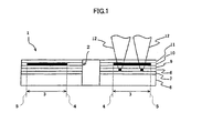
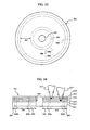
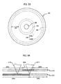
- an optical disk (optical storage medium) 1 of the present embodiment has a center hole 2 at its center and a recordable area 3 relatively close to the circumference in relation to the center hole 2.
- a spiral read/write guiding groove is formed enabling data readout and write.
- Broken lines in the figure indicates an innermost part 4 and an outermost part 5 of the recordable area 3.
- the first storage layer 10 is made up of, for example, a ZnS-SiO 2 interference film 20, a SiN protective film 21, a GeSbTe phase change recording layer 22, a SiN protective film 23, and a ZnS-SiO 2 interference film 24. These layers are sequentially stacked on the guiding-groove-formed intermediate layer 9 by sputtering.
- the optical disk 1 of the present embodiment has the guiding-groove-formed layer 7 with the guiding groove 13, and the guiding-groove-formed layer 7 is formed by 2P method.
- the optical disk 1 may be formed by preparing the disk substrate 6 by injection molding and directly forming the guiding groove 13 on the optical disk substrate 6, in which case the guiding-groove-formed layer 7 is unnecessary.
- optical-disk-read/write apparatus to read/write data on the optical disk 1 has the structure shown in Figure 5 .
- the optical disk 1 is fixed to the spindle 33 of the motor at the center hub and rotated.
- the optical-disk-read/write apparatus 31 includes an optical system unit 34 and a signal processing and controlling unit (controlling means) 35.
- the optical system unit 34 includes an illumination source 41, such as a semiconductor laser, a collimator lens 42, a beam splitter 43, an objective lens 44, a double-axis actuator 45, a collective lens 46 and a light-receiving element 47.
- the objective lens 44 is supported by the double-axis actuator 45 and moved along a focusing direction and a tracking direction.
- the light-receiving element 47 includes a reproduction signal detecting element, a focus error signal detecting element, and a tracking error signal detecting element. The outputs of the detecting elements are fed to the signal processing and controlling unit 35.
- the light beam 12 is concentrated on either the first storage layer 10 or the second storage layer 8 by the mechanism discussed in the foregoing, so that data is read/written from/into either the first storage layer 10 or the second storage layer 8 along the guiding groove 13.
- the light beam 12 emitted by the illumination source 41 is collimated by the collimator lens 42, transmitted through the beam splitter 43, before entering the objective lens 44. Then, the light beam 12 is focused by the objective lens 44 on either the first storage layer 10 or the second storage layer 8 of the optical disk 1. The reflection from the optical disk 1 passes through the objective lens 44, deflected by the beam splitter 43, and focused by the collective lens 46 on the light-receiving element 47.
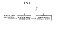
- a recording status managing signal is reproduced from data recorded in a recording status managing area of the optical disk 1, and the signal is all recorded in the write-start address producing circuit 81 in the signal processing and controlling unit 35.
- the recording status managing area is provided at a particular position in the first storage layer 10.
- the recording status managing area may contain the title of the recorded material, as well as an address representing a recording range.
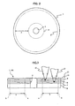
- the optical disk 61 of the present embodiment has extended areas 62 in the innermost part 4a and the outermost part 5a of the recordable area 3a of the first storage layer 10 as shown in Figures 9, 10 . Therefore, the innermost part 4a of the first storage layer 10 extends further inwards in relation to the diameter of the optical disk 1 when compared to the innermost part 4b of the second storage layer 8. The outermost part 5a of the first storage layer 10 extends further outwards in relation to the diameter when compared to the outermost part 5b of the second storage layer 8.
- Figure 11 shows an optical disk for comparison to explain the functions of the optical disk 61.
- the recordable area of the first storage layer 10 is as large as that of the second storage layer 8.
- the innermost part 4 and the outermost part 5 in the first storage layer 10 are positioned directly above and occupy the same area as their equivalents of the second storage layer 8.
- the first storage layer 10 and the second storage layer 8 each have a guiding groove 13, and the first storage layer 10 is fully recorded along the guiding groove 13 up to either the innermost part 4a, 4 or the outermost part 5a, 5 of the recordable area 3a, 3.
- the fully recorded status of the guiding groove 13 is shown by bold lines.
- the optical-disk-read/write apparatus 31 again, first writes data in the recordable area 3a, 3 of the first storage layer 10 to its full capacity before data is read/written in the recordable area 3b, 3 of the second storage layer 8.
- the light beam 12c if projected close to the innermost part 4 or the outermost part 5 of the second storage layer 8, does not entirely passes through the recordable area (fully recorded area) 3 where the first storage layer 10 exhibits a relatively high transmittance, but partially passes through unrecordable areas 64 other than the recordable area 3 where the first storage layer 10 exhibits a relatively lower transmittance. Accordingly, the light beam 12c is less intense than the light beam 12b. Therefore, in reading/writing data in the second storage layer 8, the light beam decreases, i.e., varies, in intensity in the innermost part 4, the outermost part 5, and their neighborhoods of the recordable area 3 of the second storage layer 8, making it difficult to perform stable read/write operations across the entire recordable area 3 of the second storage layer 8.
- the light beam projected on the recordable area 3b of the second storage layer 8 always becomes the light beam 12b which has passed through the recordable area (fully recorded) 3a where the first storage layer 10 exhibits a relatively high transmittance.
- the light beam does not vary in intensity whether data is read/written from/into any part of the recordable area 3b of the second storage layer 8. Stable read/write operations are thus achieved.
- An optical disk 71 of the present embodiment is operational with the optical-disk-read/write apparatus 31 which works as described in the foregoing.
- the optical-disk-read/write apparatus 31 first writes data in the first storage layer 10, and only after the recordable area 3 is recorded to its full capacity, starts writing or reading in recordable area 3 of the second storage layer 8, in which case, the pseudo-recording area 72 is already fully recorded.
- the optical-disk-read/write apparatus 31 forms a pseudo-recording area 72 by fully recording the extended area 62 prior to ordinary recording in the first storage layer 10, for example, when the optical disk 61 is loaded into the optical-disk-read/write apparatus 31.
- the optical-disk-read/write apparatus 31 first reads data from an extended area 62 of the loaded optical disk 61, and if the extended area 62 is not fully recorded, records data in the area 62 to its full capacity. The process is controlled by the signal processing and controlling unit 35 of the optical-disk-read/write apparatus 31.
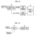
- the signal processing and controlling unit 35 is provided with the encrypting circuit 84 and the illuminating-unit-controlling circuit 82 as shown in Figure 15 .
- the encryption code information is reproduced which is recorded in advance in the pseudo-recording area 72 of the optical disk 71.
- the encrypting circuit 84 encrypts recording information based on the encryption code information and supplies the encrypted recording information to the illuminating-unit-controlling circuit 82.
- the illuminating-unit-controlling circuit 82 controls the illuminating unit so that the recording information is recorded on the optical disk 71.
- the pseudo-recording area 72 contains disk identification information, it is possible to prevent the illegal copying and other uses of the optical disk 71 by managing the disk identification information in the optical-disk-read/write apparatus 31 or in a server or the like connected to the optical-disk-read/write apparatus 31.
- the managing of the disk identification information refers to the processing to count the times the optical disk 71 is used to limit the times the disk is used, for example.
- the optical-disk-read/write apparatus 31 may record, in the pseudo-recording area 72, the apparatus ID information which is unique to the optical-disk-read/write apparatus 31 or encryption code information which is unique to the optical-disk-read/write apparatus 31.
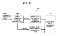
- the signal processing and controlling unit 35 in the optical-disk-read/write apparatus 31 is equipped with an encryption-information-presence-checking circuit 86 and the illuminating-unit-controlling circuit 82 as shown in
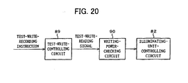
- the extended area 62 of the optical disk 61 can be used as a test write area as follows.
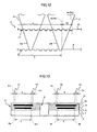
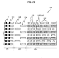
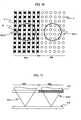
- the recording marks 111 have a higher transmittance. Therefore, referring to Figure 22 , the light beam 12e projected onto the second storage layer 8 after passing trough a portion of the first storage layer 10 where the recording marks 111 are present has a greater intensity than the light beam projected onto the second storage layer 8 without passing through that portion where the recording marks 111 are present. Likewise, since the address area 104 on the first storage layer 10 has continuous storage areas 114, the light beam 12f projected onto the second storage layer 8 after passing through the address area 104 has a greater intensity than the light beam projected onto the second storage layer 8 after passing through the address area in the case where there are no continuous storage areas 114.
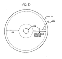
- a continuous storage area 114 appears on alternate address tracks 113 in relation to a diameter of the optical disk 101. Therefore, when the light beam 12 is focused on the second storage layer 8 as shown in Figure 22 , in the case where a beam spot 115 formed by the light beam 12 forms on the first storage layer 10 as shown in Figure 21 , the sum of the areas of the recording marks 111 included in the area of the beam spot 115 in the non-address area 105 on the first storage layer 10 is substantially equal to the sum of the continuous storage areas 114 included in the area of the beam spot 115 in the address area 104.
- Figure 21 ten address pits 112 are shown forming an address track 113.
- Figure 21 is only a schematic figure, and in practice, an address track 113 is made up of 1000 or more address pits 112 of various lengths.
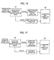
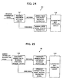
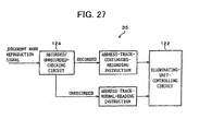
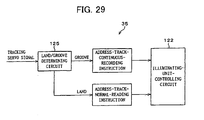
- the signal processing and controlling unit 35 in the optical-disk-read/write apparatus 31 has a recorded/unrecorded switching circuit 121 and an illuminating-unit-controlling circuit 122 as shown in Figure 24 .
- the illuminating unit controlled by the illuminating-unit-controlling circuit 122 is inclusive of an optical system unit 34 and a slide driving unit.
- the recorded/unrecorded switching circuit 121 feeds an address-track-continuous-recording-instructing signal to the illuminating-unit-controlling circuit 122.
- the illuminating-unit-controlling circuit 122 controls the illuminating unit and continuously record the address track 113.
- the subsequent-address-track-recorded/unrecorded checking circuit 123 determines based on the address information obtained from the address area 104 whether to make the address track 113 a continuous storage area 114.
- the address information obtained from the address area 104 determines whether to make the address track 113 a continuous storage area 114.
- that address track 113 is read first of all, and it is determined based on the obtained address information whether to make a subsequent address track 113 a continuous storage area 114.
- the recorded/unrecorded-checking circuit 124 fees an address-track-normal-reading-instructing signal to the illuminating-unit-controlling circuit 122.
- the illuminating-unit-controlling circuit 122 controls the illuminating unit so as to read the address track 113 at a laser intensity which is incapable of recording data.
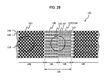
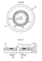
- the address area 104 is made up of a first address area 144 and a second address area 145 which are adjacent to each other along tracks.
- first address pits 146 along imaginary lines extending from the groove 142.
- second address pits 147 along imaginary lines extending from the land 143. Relatively shifting the positions of the first address area 144 and the second address area 145 along the tracks so that they do not overlap in a direction normal to the tracks eliminates crosstalk in signals reproduced from the first and second address pits 146, 147.
- the positions of the first address area 144 and the second address area 145 may be reversed.
- the continuous storage area 114 may be formed in the second address area 145 in those address tracks 113 which extend from the groove 142, in the first address area 144 in those address tracks 113 which extend from the land 143, and in each address track 113.
- the first address area 144 and the second address area 145 may be reversed in position.
- the continuous storage area 114 may be formed only at places where the first address pit 146 and the second address pit 147 are provided, conversely to the formation places in Figure 30 .
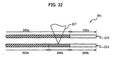
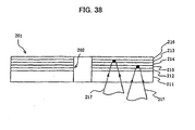
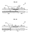
- a light beam 217 projected from one side of the disk i.e., the side on which the surface-coating layer 216 exists, is concentrated on the first and second storage layers 215, 213.
- the surface-coating layer 216 is made of, for example, a 80-micron thick, ultraviolet-ray-setting resin layer, and formed by spin coating the first storage layer 215 with an ultraviolet-ray-setting resin and setting the resin by the projection of ultraviolet rays.
- the optical disk 201 has a structure including the guiding-groove-and-pits-formed layer 212, the second storage layer 213, the guiding-groove-and-pits-formed intermediate layer 214, the first storage layer 215, and the surface-coating layer 216 sequentially stacked on the optical disk substrate 211. This is not the only option available.
- the optical-disk-read/write apparatus 31 reads from, or writes into, the second storage layer 213 after the recordable area 203 of the first storage layer 215 is fully recorded.
- the operations in this case are carried out under the control of the signal processing and controlling unit 35 on the optical system unit (illuminating means) 34 and the slide driving unit (illuminating means).
- Figure 62 shows the first storage layer 215 and the second storage layer 213 near the periphery of the optical disk 201 in their initial states.
- the first storage layer 215 has an unrecorded recordable area 203a and a blank area 205a constituting the outermost part 205
- the second storage layer 213 has an unrecorded recordable area 203b, an outer prepit area 206a, and a blank area 205b constituting the outermost part 205.
- the blank areas 205a, 205b are those areas where no guiding groove G or pits P are formed.
- the innermost part 204 of the first and second storage layers 215, 213 also has similar blank areas (not shown).
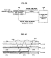
- the pseudo-recording area 207 is read immediately after the optical disk 201 is loaded in the optical-disk-read/write apparatus 31.
- the pseudo-recording-status-checking circuit 271 checks based on the reproduction signal whether the pseudo-recording area 207 is fully recorded or not.
- the pseudo-recording-status-checking circuit 271 regards the loaded optical disk 201 as having been used, and feeds an ordinary writing-instruction signal to the illuminating-unit-controlling circuit 36. As a result, an ordinary recording operation is performed as to the optical disk 201 under the control of the illuminating-unit-controlling circuit 36.
- the recordable area 203a of the first storage layer 215 should be than the recordable area 203b of the second storage layer 213.
- the first storage layer 215 is separated from the second storage layer 213 by a distance of 20 microns
- the light beam 217j focused on the second storage layer 213 forms on the first storage layer 215 a spot having a radius of about 10 microns. Therefore, the recordable area 203b needs be formed at least about 10 microns wider than the width of the recordable area 203a.
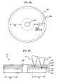
- alternate pit rows of pits P which are spirally (or concentrically) arranged have a continuously recorded, continuous storage area R.
- the pits P and the intervals between the pits P are continuously in the same state, i.e., have the same transmittance, as the recording marks M in the recordable area 203a.
- the non-recorded area between any adjacent pit rows is formed substantially as wide as the diameter of the pit P. Therefore, to form a recorded portion (1/4 the net prepit area 208) which has an area substantially equal to the recorded portion of the recordable area 203a, recording needs be done so that a continuous storage area R can be formed for alternate pit rows.
- the continuous storage area R may be formed in the pit row in the prepit area 208 either prior to the shipment of the optical disk 201 or by using the optical-disk-read/write apparatus 31 when an unused optical disk 201 is loaded into the optical-disk-read/write apparatus 31.
- the formation of the continuous storage area R using the optical-disk-read/write apparatus 31 eliminates the need to form the continuous storage area R prior to the shipment of the optical disk 201, and reduces the cost of the optical disk 201.
- Figure 59 shows a configuration to form a continuous storage area R in the pit row in the prepit area 208 using the optical-disk-read/write apparatus 31 in the foregoing manner.
- the configuration includes the aforementioned continuous-storage-area-presence-checking circuit 291 provided in the signal processing and controlling unit 35.
- the optical disk 201 similarly to the optical disk 201 shown in Figure 62 , in reading data from a prepit area 206 in the third storage layer 218.
- the quantity of light reflected off a prepit area 206 varies depending upon whether the first storage layer 215 and the second storage layer 213 through which light beams 217m, 217n pass are fully recorded or not.
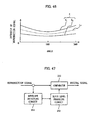
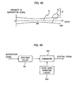
- a slice level can be produced from the envelope of a reproduction signal by using the reproduction circuit shown in Figure 47 . Obtaining a digital signal with the slice level as a reference, prepit information can be reproduced stably.
- An optical read/write method of the present invention is arranged to include the steps of: preparing the optical storage medium; preparing encryption information by which data is encrypted before being stored in the optical storage medium; and storing the encryption information in the extended area.
- An optical read/write apparatus of the present invention causes a read/write light beam from illuminating means to strike only one side of the optical storage medium and is arranged so as to include controlling means for controlling the illuminating means so as to test write data in the extended area.
- An optical read/write method of the present invention is arranged to include the steps of preparing the optical storage medium, and test writing data in the extended area.
- An optical storage medium of the present invention includes stacked multiple data storage layer each of which is readable/writeable separately from the other data storage layers by means of only a light beam striking one side of the optical storage medium, each of the data storage layers having address tracks and at least one address area where there are collectively formed address information portions representing address information, the optical storage medium exhibiting an optical transmittance which varies when data is written by means of the incident light, and is arranged so that one of every adjacent two of the address tracks in the address area of a first data storage layer is continuously recorded by means of the incident light, and the other is unrecorded, the first data storage layer being one of the data storage layers which is located closest to a light-striking surface of the optical storage medium, a second data storage layer being another of the data storage layers which is located next to the first data storage layer, opposite the light-striking surface.
- an optical read/write apparatus of the present invention causes a read/write light beam from illuminating means to strike only one side of an optical storage medium including multiple stacked data storage layers each of which is readable/writeable separately from the other data storage layers by means of only a light beam striking one side of the optical storage medium, each of the data storage layers having multiple address tracks and at least one address area where there are collectively formed address information portions representing address information, the optical storage medium exhibiting an optical transmittance which varies when data is written by means of the light beam, and is arranged so that the optical read/write apparatus includes controlling means for controlling the illuminating means so that one of every adjacent two of the address tracks in the address area of a first data storage layer is continuously recorded by means of the incident light, and the other one is unrecorded, the first data storage layer being one of the data storage layers which is located closest to a light-striking surface of the medium, a second data storage layer being another of the data storage layers which is located next to the first data storage layer; opposite the light-s
- an optical read/write method of the present invention includes the step of causing a read/write light beam to strike only one side of an optical storage medium including multiple stacked data storage layers each of which is readable/writeable separately from the other data storage layers by means of only a light beam striking one side of the optical storage medium, each of the data storage layers having multiple address tracks and at least one address area where there are collectively formed address information portions representing address information, the optical storage medium exhibiting an optical transmittance which varies when data is written by means of the light beam, and is arranged so as to further include the step of continuously recording one of every adjacent two of the address tracks in the address area of a first data storage layer by means of the incident light, while leaving the other one unrecorded, the first data storage layer being one of the data storage layers which is located closest to a light-striking surface of the medium, a second data storage layer being another of the data storage layers which is located next to the first data storage layer, opposite the light-striking surface.
- the arrangement one of every adjacent two of the address tracks in the address area of the first data storage layer located close to the light-striking surface of the optical storage medium is continuously recorded by means of the incident light, and the other is unrecorded. Therefore, in reading/writing in the second data storage layer, in a case where the light projected to focus on the second data storage layer forms a light spot on the first data storage layer, the recorded area encompassed in the light spot of a non-address area in the recordable area of the first data storage layer, for example, the sum of the areas of the recording marks, is substantially equal to the sum of the continuously recorded areas encompassed in the light spot in the address area of the first data storage layer.
- the intensity of light transmitted through the address area of the first data storage layer before reaching the second data storage layer can be made substantially equal to the intensity of light transmitted through the non-address area in the recordable area of the first data storage layer before reaching the second data storage layer.
- read/write operations on the second data storage layer become more stable and desirable.
- an optical read/write method of the present invention includes the step of causing a read/write light beam from illuminating means to strike only one side of the optical storage medium, and is arranged so as to further include the steps of removing low frequency variations from the reproduction signal obtained from the prepit area; and converting the reproduction signal from which the low frequency variations are removed to a digital signal using a constant voltage as a reference.
- the prepit area allows light to be transmitted at a transmittance substantially equal that as the transmittance of the recordable area of the light-striking side storage layer, the light passing through the recordable area and through the prepit area has substantially the same intensity. Therefore, data can be read from and written to the last data storage layer stably without being affected by the prepit area.
- the recordable areas come to have higher optical transmittances than other areas upon completion of recording. Therefore, keeping the recordable area fully recorded enables the light passing through the recordable areas to remain sufficiently intense until it reaches a target data storage layer. Therefore, data can be stably read and written on an optical storage medium with multiple storage layers.
- the controlling means controls the illuminating means so that the recordable area of the light-striking side storage layer fully recorded before the recordable area of a target opposite-side storage layer is read or written. Therefore, in reading or writing the opposite-side storage layers, the light passing through the light-striking side storage layer remains sufficiently intense until it reaches the opposite-side storage layers. Therefore, data can be stably read and written on the optical storage medium.
Landscapes
- Engineering & Computer Science (AREA)
- Physics & Mathematics (AREA)
- Optics & Photonics (AREA)
- Computer Security & Cryptography (AREA)
- Signal Processing (AREA)
- Power Engineering (AREA)
- Optical Recording Or Reproduction (AREA)
Claims (2)
- Optische Lese-/Schreibvorrichtung
mit:Beleuchtungsmitteln (34), um ein Lese-/Schreib-Lichtstrahlenbündel zu liefern; undMitteln (32, 33) zum Montieren eines optischen Speichermediums, um ein optisches Speichermedium (1, 201) in der Weise zu tragen, dass das Lese-/Schreib-Lichtstrahlenbündel von den Beleuchtungsmitteln (34) nur auf eine Lichtauftreffseite des optischen Speichermediums (1, 201) auftrifft,wobei:das optische Speichermedium (1, 201) scheibenförmig ausgebildet ist und gestapelte Datenspeicherschichten (8, 10) aufweist, wovon jede getrennt von den anderen Schichten mittels eines Lichtstrahlenbündels, das auf die Lichtauftreffseite des optischen Speichermediums (1, 201) auftrifft, lesbar/beschreibbar ist,das optische Speichermedium in der Weise strukturiert und konfiguriert ist, dass ein aufzeichnungsfähiger Bereich (3a) der ersten Datenspeicherschicht (10), der wenigstens einen Abschnitt (62) mit aufzeichnungsfähigem erweitertem Bereich aufweist, in einer Richtung, in der die erste und eine zweite Datenspeicherschicht (8, 10) gestapelt sind, über der zweiten Datenspeicherschicht (8) vorgesehen ist und der wenigstens eine Abschnitt (62) mit aufzeichnungsfähigem erweitertem Bereich sich in einer radialen Richtung des optischen Speichermediums über einen vollständigen aufzeichnungsfähigen Bereich der zweiten Datenspeicherschicht (8) hinaus erstreckt, wobei eine Länge des wenigstens einen Abschnitts (62) mit aufzeichnungsfähigem erweitertem Bereich in radialer Richtung des optischen Speichermediums (1, 201) gleich oder größer ist als eine Dicke einer Zwischenschicht, die zwischen der ersten Datenspeicherschicht (10) und der zweiten Datenspeicherschicht (8) vorgesehen ist, zuzüglich eines Betrags, der zu einer Exzentrizität zwischen der ersten Datenspeicherschicht (10) und der zweiten Datenspeicherschicht (8) äquivalent ist, und wobei ferner:die zweite Datenspeicherschicht (8) sich von der Lichtauftreffoberfläche des optischen Speichermediums (1, 201) am weitesten entfernt befindet und die erste Datenspeicherschicht (10) sich am nächsten bei der zweiten Datenspeicherschicht (8) näher bei der Lichtauftreffoberfläche befindet,wobei die optische Lese-/Schreibvorrichtung das optische Speichermedium (1, 201) verwendet unddadurch gekennzeichnet,dass die optische Lese-/Schreibvorrichtung ferner Steuermittel (82) aufweist, um die Beleuchtungsmittel (34) in der Weise zu steuern, dass ein Testschreibvorgang auf der ersten Datenspeicherschicht (10) auf dem wenigstens einen Abschnitt (62) des aufzeichnungsfähigen erweiterten Bereichs ausgeführt wird. - Optische Lesevorrichtung
mit:Beleuchtungsmitteln (34), um ein Lese-Lichtstrahlenbündel zu liefern;
undMitteln (32, 33) zum Montieren eines optischen Speichermediums, um ein optisches Speichermedium (1, 201) in der Weise zu tragen, dass das Lese-Lichtstrahlenbündel von den Beleuchtungsmitteln (34) nur auf eine Lichtauftreffseite des optischen Speichermediums (1, 201) auftrifft,wobei:das optische Speichermedium (1, 201) scheibenförmig ausgebildet ist und gestapelte Datenspeicherschichten (8, 10) aufweist, wovon jede getrennt von den anderen Schichten mittels eines Lichtstrahlenbündels, das auf die Lichtauftreffseite des optischen Speichermediums (1, 201) auftrifft, lesbar/beschreibbar ist,das optische Speichermedium in der Weise strukturiert und konfiguriert ist, dass ein aufzeichnungsfähiger Bereich (3a) der ersten Datenspeicherschicht (10), der wenigstens einen Abschnitt (62) mit aufzeichnungsfähigem erweitertem Bereich aufweist, in einer Richtung, in der die erste und eine zweite Datenspeicherschicht (8, 10) gestapelt sind, über der zweiten Datenspeicherschicht (8) vorgesehen ist und der wenigstens eine Abschnitt (62) mit aufzeichnungsfähigem erweitertem Bereich sich in einer radialen Richtung des optischen Speichermediums über einen vollständigen aufzeichnungsfähigen Bereich der zweiten Datenspeicherschicht (8) hinaus erstreckt, wobei eine Länge des wenigstens einen Abschnitts (62) mit aufzeichnungsfähigem erweitertem Bereich in radialer Richtung des optischen Speichermediums (1, 201) gleich oder größer ist als eine Dicke einer Zwischenschicht, die zwischen der ersten Datenspeicherschicht (10) und der zweiten Datenspeicherschicht (8) vorgesehen ist, zuzüglich eines Betrags, der zu einer Exzentrizität zwischen der ersten Datenspeicherschicht (10) und der zweiten Datenspeicherschicht (8) äquivalent ist, und wobei ferner:die zweite Datenspeicherschicht (8) sich von der Lichtauftreffoberfläche des optischen Speichermediums (1, 201) am weitesten entfernt befindet und die erste Datenspeicherschicht (10) sich am nächsten bei der zweiten Datenspeicherschicht (8) näher bei der Lichtauftreffoberfläche befindet,wobei die optische Lesevorrichtung das optische Speichermedium (1, 201) verwendet unddadurch gekennzeichnet,dass die Beleuchtungsmittel (34) der zweiten Speicherschicht (8) ein Lese-Lichtstrahlenbündel über den aufzeichnungsfähigen Bereich (3a) zuführen, der den wenigstens einen Abschnitt (62) des aufzeichnungsfähigen erweiterten Bereichs, der als ein Testschreibbereich zugewiesen ist, enthält.
Applications Claiming Priority (4)
| Application Number | Priority Date | Filing Date | Title |
|---|---|---|---|
| JP2001150177A JP2002342926A (ja) | 2001-05-18 | 2001-05-18 | 光記録媒体、光記録再生装置および光記録再生方法 |
| JP2001150173A JP4040265B2 (ja) | 2001-05-18 | 2001-05-18 | 光記録媒体、光記録再生装置および光記録再生方法 |
| JP2001179330A JP2002373426A (ja) | 2001-06-13 | 2001-06-13 | 光記録媒体、光記録再生装置および光記録再生方法 |
| EP02010885A EP1258868B8 (de) | 2001-05-18 | 2002-05-15 | Optisches Speichermedium, optische Lese- /Schreibvorrichtung, und optisches Lese- /Schreibverfahren |
Related Parent Applications (1)
| Application Number | Title | Priority Date | Filing Date |
|---|---|---|---|
| EP02010885.8 Division | 2002-05-15 |
Publications (3)
| Publication Number | Publication Date |
|---|---|
| EP2226800A2 EP2226800A2 (de) | 2010-09-08 |
| EP2226800A3 EP2226800A3 (de) | 2010-11-03 |
| EP2226800B1 true EP2226800B1 (de) | 2012-07-11 |
Family
ID=27346752
Family Applications (8)
| Application Number | Title | Priority Date | Filing Date |
|---|---|---|---|
| EP10003582A Expired - Lifetime EP2224437B1 (de) | 2001-05-18 | 2002-05-15 | Optisches Speichermedium, optische Lese-/Schreibvorrichtung und optisches Lese-/Schreibverfahren |
| EP10003634A Expired - Lifetime EP2261903B9 (de) | 2001-05-18 | 2002-05-15 | Optisches Speichermedium |
| EP12000615.0A Expired - Lifetime EP2461326B1 (de) | 2001-05-18 | 2002-05-15 | Optisches Speichermedium, optische Lese-/Schreibvorrichtung und optisches Lese-/Schreibverfahren |
| EP10003633A Expired - Lifetime EP2261902B1 (de) | 2001-05-18 | 2002-05-15 | Optisches Speichermedium, optische Lese-/Schreibvorrichtung und optisches Lese-/Schreibverfahren |
| EP02010885A Expired - Lifetime EP1258868B8 (de) | 2001-05-18 | 2002-05-15 | Optisches Speichermedium, optische Lese- /Schreibvorrichtung, und optisches Lese- /Schreibverfahren |
| EP10003609A Expired - Lifetime EP2226800B1 (de) | 2001-05-18 | 2002-05-15 | Optisches Speichermedium, optische Lese-/Schreibvorrichtung und optisches Lese-/Schreibverfahren |
| EP12000614.3A Expired - Lifetime EP2461325B1 (de) | 2001-05-18 | 2002-05-15 | Optisches Speichermedium, optische Lese-/Schreibvorrichtung und optisches Lese-/Schreibverfahren |
| EP10003583A Expired - Lifetime EP2226799B1 (de) | 2001-05-18 | 2002-05-15 | Optisches Speichermedium, optische Lese-/Schreibvorrichtung und optisches Lese-/Schreibverfahren |
Family Applications Before (5)
| Application Number | Title | Priority Date | Filing Date |
|---|---|---|---|
| EP10003582A Expired - Lifetime EP2224437B1 (de) | 2001-05-18 | 2002-05-15 | Optisches Speichermedium, optische Lese-/Schreibvorrichtung und optisches Lese-/Schreibverfahren |
| EP10003634A Expired - Lifetime EP2261903B9 (de) | 2001-05-18 | 2002-05-15 | Optisches Speichermedium |
| EP12000615.0A Expired - Lifetime EP2461326B1 (de) | 2001-05-18 | 2002-05-15 | Optisches Speichermedium, optische Lese-/Schreibvorrichtung und optisches Lese-/Schreibverfahren |
| EP10003633A Expired - Lifetime EP2261902B1 (de) | 2001-05-18 | 2002-05-15 | Optisches Speichermedium, optische Lese-/Schreibvorrichtung und optisches Lese-/Schreibverfahren |
| EP02010885A Expired - Lifetime EP1258868B8 (de) | 2001-05-18 | 2002-05-15 | Optisches Speichermedium, optische Lese- /Schreibvorrichtung, und optisches Lese- /Schreibverfahren |
Family Applications After (2)
| Application Number | Title | Priority Date | Filing Date |
|---|---|---|---|
| EP12000614.3A Expired - Lifetime EP2461325B1 (de) | 2001-05-18 | 2002-05-15 | Optisches Speichermedium, optische Lese-/Schreibvorrichtung und optisches Lese-/Schreibverfahren |
| EP10003583A Expired - Lifetime EP2226799B1 (de) | 2001-05-18 | 2002-05-15 | Optisches Speichermedium, optische Lese-/Schreibvorrichtung und optisches Lese-/Schreibverfahren |
Country Status (4)
| Country | Link |
|---|---|
| US (10) | US7180849B2 (de) |
| EP (8) | EP2224437B1 (de) |
| KR (1) | KR100495678B1 (de) |
| ES (6) | ES2390415T3 (de) |
Families Citing this family (34)
| Publication number | Priority date | Publication date | Assignee | Title |
|---|---|---|---|---|
| US7180849B2 (en) * | 2001-05-18 | 2007-02-20 | Sharp Kabushiki Kaisha | Optical storage medium enabling uniform light transmittance, optical read/write apparatus for same, and optical read/write method for same |
| CN1659656B (zh) | 2002-06-10 | 2010-06-16 | 皇家飞利浦电子股份有限公司 | 用于对多层光盘进行写入的方法和设备 |
| US20040120241A1 (en) * | 2002-10-18 | 2004-06-24 | Isao Kobayashi | Method and apparatus of recording optical information |
| JP3710790B2 (ja) * | 2003-03-24 | 2005-10-26 | 株式会社リコー | 情報記録方法及びその装置 |
| JP2005032413A (ja) * | 2003-06-19 | 2005-02-03 | Nec Corp | 光ディスクの未記録領域への記録方法、光デイスクの記録装置,光ディスク及び光ディスクのデータ記録用プログラム |
| KR100677114B1 (ko) * | 2004-04-27 | 2007-02-02 | 삼성전자주식회사 | 정보 저장 매체, 이 정보 저장 매체의 데이터 기록/재생방법 및 장치 |
| TWI368218B (en) * | 2004-06-11 | 2012-07-11 | Pioneer Corp | Information recording apparatus and method |
| KR100667755B1 (ko) * | 2004-06-23 | 2007-01-11 | 삼성전자주식회사 | 복수의 기록층을 구비한 광 디스크, 데이터 기록 방법 및그 장치 |
| US7539113B2 (en) | 2004-08-30 | 2009-05-26 | Pioneer Corporation | Information recording apparatus and computer program |
| JP4622454B2 (ja) * | 2004-10-28 | 2011-02-02 | Tdk株式会社 | 多層光記録媒体 |
| JP4254688B2 (ja) * | 2004-10-29 | 2009-04-15 | ティアック株式会社 | 光ディスク装置及びそのデータ記録装置 |
| JP4107290B2 (ja) * | 2004-12-24 | 2008-06-25 | ティアック株式会社 | 光ディスク装置 |
| WO2006073079A1 (ja) * | 2005-01-06 | 2006-07-13 | Pioneer Corporation | 記録装置及び記録方法、並びにコンピュータプログラム |
| JP2006236420A (ja) | 2005-02-22 | 2006-09-07 | Toshiba Corp | 記憶媒体、再生方法及び記録方法 |
| JP4072546B2 (ja) * | 2005-09-12 | 2008-04-09 | 日本電気株式会社 | 2層光ディスク |
| US20090016188A1 (en) * | 2006-03-03 | 2009-01-15 | Atsushi Nakamura | Multi-layer information recording medium, information recording/reproducing device and multi-layer information recording medium manufacturing method |
| JP5024077B2 (ja) * | 2008-01-29 | 2012-09-12 | Tdk株式会社 | 多層光記録媒体の特性評価方法 |
| MX350703B (es) | 2009-05-13 | 2017-09-14 | Sio2 Medical Products Inc | Metodo de gasificacion para inspeccionar una superficie revestida. |
| WO2013170052A1 (en) | 2012-05-09 | 2013-11-14 | Sio2 Medical Products, Inc. | Saccharide protective coating for pharmaceutical package |
| US11624115B2 (en) | 2010-05-12 | 2023-04-11 | Sio2 Medical Products, Inc. | Syringe with PECVD lubrication |
| US9878101B2 (en) | 2010-11-12 | 2018-01-30 | Sio2 Medical Products, Inc. | Cyclic olefin polymer vessels and vessel coating methods |
| JP2012164372A (ja) * | 2011-02-03 | 2012-08-30 | Sony Corp | 光情報記録媒体の製造方法および光情報記録媒体 |
| JP2013033563A (ja) * | 2011-08-01 | 2013-02-14 | Sony Corp | 光記録媒体、記録再生装置、記録再生方法 |
| US11116695B2 (en) | 2011-11-11 | 2021-09-14 | Sio2 Medical Products, Inc. | Blood sample collection tube |
| EP2776603B1 (de) | 2011-11-11 | 2019-03-06 | SiO2 Medical Products, Inc. | Passivierungs-, ph-schutz- oder schmierbeschichtung für arzneimittelverpackung, beschichtungsverfahren und vorrichtung |
| US20150297800A1 (en) | 2012-07-03 | 2015-10-22 | Sio2 Medical Products, Inc. | SiOx BARRIER FOR PHARMACEUTICAL PACKAGE AND COATING PROCESS |
| CA2890066C (en) | 2012-11-01 | 2021-11-09 | Sio2 Medical Products, Inc. | Coating inspection method |
| US9903782B2 (en) | 2012-11-16 | 2018-02-27 | Sio2 Medical Products, Inc. | Method and apparatus for detecting rapid barrier coating integrity characteristics |
| US9764093B2 (en) | 2012-11-30 | 2017-09-19 | Sio2 Medical Products, Inc. | Controlling the uniformity of PECVD deposition |
| JP6382830B2 (ja) | 2012-11-30 | 2018-08-29 | エスアイオーツー・メディカル・プロダクツ・インコーポレイテッド | 医療シリンジ、カートリッジ等上でのpecvd堆積の均一性制御 |
| EP2971228B1 (de) | 2013-03-11 | 2023-06-21 | Si02 Medical Products, Inc. | Beschichtete verpackung |
| US9937099B2 (en) | 2013-03-11 | 2018-04-10 | Sio2 Medical Products, Inc. | Trilayer coated pharmaceutical packaging with low oxygen transmission rate |
| WO2015148471A1 (en) | 2014-03-28 | 2015-10-01 | Sio2 Medical Products, Inc. | Antistatic coatings for plastic vessels |
| EP3337915B1 (de) | 2015-08-18 | 2021-11-03 | SiO2 Medical Products, Inc. | Pharmazeutische und andere verpackungen mit niedriger sauerstoffübertragungsrate |
Family Cites Families (58)
| Publication number | Priority date | Publication date | Assignee | Title |
|---|---|---|---|---|
| US223542A (en) * | 1880-01-13 | Vehicle-spring | ||
| US6728A (en) * | 1849-09-18 | Coupling fob cabs | ||
| US1111604A (en) * | 1911-05-04 | 1914-09-22 | Continental & Commercial Trust & Savings Bank | Bed-motion in printing-machines. |
| US1176586A (en) * | 1915-03-11 | 1916-03-21 | Oliver P Megahan | Curtain-clamp. |
| US2075728A (en) * | 1935-07-01 | 1937-03-30 | Delamere Co Inc | Bow holder |
| US3157816A (en) * | 1962-12-31 | 1964-11-17 | Burroughs Corp | Beam switching tube counting circuit with particular transfer means between electrode groups |
| DE2504970A1 (de) * | 1975-02-06 | 1976-08-26 | Barmag Barmer Maschf | Flachfolien - kuehlvorrichtung |
| US4827462A (en) * | 1987-03-26 | 1989-05-02 | International Business Machines Corporation | Modular data storage directories for large-capacity data storage units |
| US5303225A (en) * | 1989-10-30 | 1994-04-12 | Matsushita Electrical Industrial Co., Ltd. | Multi-layered optical disk with track and layer identification |
| JP2928292B2 (ja) | 1989-11-15 | 1999-08-03 | 松下電器産業株式会社 | 光学情報記録部材および光学情報記録再生装置 |
| JP2997512B2 (ja) * | 1990-07-13 | 2000-01-11 | 株式会社東芝 | 多層光記録媒体 |
| JP3243800B2 (ja) * | 1991-06-07 | 2002-01-07 | ソニー株式会社 | 光ディスク媒体のグレーコードの形成方法及びトラックアドレス再生装置 |
| JP3266627B2 (ja) | 1991-10-11 | 2002-03-18 | 株式会社日立製作所 | 情報再生装置 |
| CN1132185C (zh) * | 1994-12-19 | 2003-12-24 | 皇家菲利浦电子有限公司 | 多层记录载体和扫描该载体的装置 |
| JP3467964B2 (ja) * | 1995-08-10 | 2003-11-17 | ソニー株式会社 | データ記録装置及び方法、データ再生装置及び方法、記録媒体、並びにデータ伝送方法 |
| JP3076230B2 (ja) | 1995-10-13 | 2000-08-14 | 日本電気株式会社 | 光ディスク |
| JPH09231613A (ja) | 1996-02-26 | 1997-09-05 | Nippon Columbia Co Ltd | 光情報記録媒体 |
| US5804585A (en) * | 1996-04-15 | 1998-09-08 | Texas Biotechnology Corporation | Thieno-pyridine sulfonamides derivatives thereof and related compounds that modulate the activity of endothelin |
| JP2983920B2 (ja) * | 1996-06-18 | 1999-11-29 | 三洋電機株式会社 | 互換再生可能なピックアップ調整用光記録媒体およびその調整方法 |
| US5914826A (en) * | 1996-07-24 | 1999-06-22 | Logic Laboratories, Inc. | Light switch cover plate with audio recording and playback feature |
| JPH1049104A (ja) * | 1996-07-31 | 1998-02-20 | Pioneer Electron Corp | プラズマディスプレイ装置 |
| JP2002504258A (ja) * | 1997-06-16 | 2002-02-05 | トムソン コンシユーマ エレクトロニクス インコーポレイテツド | 記録媒体、dvdディスク、レーザ―コード化するための装置、ディスクを処理する方法、光ディスク、およびディスクの形成方法 |
| JP3110349B2 (ja) * | 1997-07-02 | 2000-11-20 | 日本電気株式会社 | フレームアライナ回路 |
| JPH1131357A (ja) * | 1997-07-08 | 1999-02-02 | Pioneer Electron Corp | 情報データの記録方法 |
| US6272086B1 (en) * | 1997-11-18 | 2001-08-07 | International Business Machines Corporation | Low cost tamper-resistant method for write-once read many (WORM) storage |
| US6720058B1 (en) * | 1997-12-05 | 2004-04-13 | E.I. Du Pont De Nemours And Company | Velour-like pile articles and pile surface structures and methods of making |
| JPH11203795A (ja) | 1998-01-06 | 1999-07-30 | Victor Co Of Japan Ltd | 光ディスクの復号装置 |
| KR100524297B1 (ko) * | 1998-03-24 | 2006-01-12 | 엘지전자 주식회사 | 재기록 가능한 디스크와 이를 이용한 기록 방법 |
| WO1999060976A1 (en) * | 1998-05-29 | 1999-12-02 | Ricon Corporation | Wheelchair lift with foldable platform |
| DE69934424T2 (de) * | 1998-10-21 | 2007-10-31 | Matsushita Electric Industrial Co., Ltd., Kadoma | Optisches informationsaufzeichnungsmedium, und verfahren und gerät zur aufzeichnung und wiedergabe |
| JP2000285469A (ja) * | 1999-03-31 | 2000-10-13 | Toshiba Corp | 光記録媒体および光記録再生装置 |
| KR100470468B1 (ko) * | 1999-04-07 | 2005-02-05 | 마쯔시다덴기산교 가부시키가이샤 | 다층 광 디스크 및 그것에 광학 정보를 기록하는 방법 및장치 |
| EP1111604A1 (de) * | 1999-06-28 | 2001-06-27 | Sony Corporation | Optisches aufzeichnungsmedium und verfahren zum lesen eines optischen aufzeichnungsmediums |
| JP2001014684A (ja) | 1999-06-30 | 2001-01-19 | Toshiba Corp | 光ディスクおよびその製造方法 |
| JP2001023254A (ja) | 1999-07-02 | 2001-01-26 | Canon Inc | 光磁気記録テスト方法及び光磁気記録再生装置 |
| JP4085530B2 (ja) | 1999-08-05 | 2008-05-14 | ソニー株式会社 | 光学記録媒体、並びに信号記録装置及び信号記録方法 |
| JP4300642B2 (ja) * | 1999-08-18 | 2009-07-22 | ソニー株式会社 | 記録媒体及び記録媒体の再生装置並びに再生方法 |
| DE60028490T2 (de) * | 1999-10-07 | 2007-06-06 | Siemens Vdo Automotive Inc., Chatham | Überdruckkurbelgehäuseentlüftungssystem |
| JP2001127640A (ja) | 1999-10-29 | 2001-05-11 | Sony Corp | 光学式回転記録媒体、データ記録方法、記録装置、再生装置 |
| JP2001209940A (ja) * | 1999-11-16 | 2001-08-03 | Victor Co Of Japan Ltd | 光ディスク記録再生装置、光ディスク記録再生方法および光ディスク |
| JP4438172B2 (ja) * | 2000-03-30 | 2010-03-24 | ソニー株式会社 | データ記録装置及びデータ記録方法 |
| DE60113346T2 (de) * | 2000-07-26 | 2006-06-22 | Kabushiki Kaisha Toshiba, Kawasaki | Aufzeichnungsträger für Informationen mit einem Indexstartfeld |
| JP2002092939A (ja) | 2000-09-12 | 2002-03-29 | Pioneer Electronic Corp | 多層光学式記録媒体及びその製造方法 |
| AU8620901A (en) | 2000-09-13 | 2002-03-26 | Matsushita Electric Industrial Co Ltd | Optical information recording medium and optical information recording method, optical information recording device |
| JP2002133714A (ja) * | 2000-10-23 | 2002-05-10 | Pioneer Electronic Corp | 多層情報記録媒体及び記録装置 |
| TW588346B (en) * | 2000-12-22 | 2004-05-21 | Koninkl Philips Electronics Nv | Multilayer record carrier and method of manufacturing thereof and recording thereon |
| US20020092939A1 (en) * | 2001-01-18 | 2002-07-18 | Sowers David A. | Hypodermic needle and syringe decontaminating and destroying apparatus |
| JP4215405B2 (ja) * | 2001-01-22 | 2009-01-28 | シャープ株式会社 | 光ディスク |
| JP2002245628A (ja) | 2001-02-14 | 2002-08-30 | Tdk Corp | 光ディスクおよび光記録再生方法 |
| JP2002260234A (ja) | 2001-03-02 | 2002-09-13 | Sony Corp | 記録再生装置および方法、記録媒体、並びにプログラム |
| JP4386594B2 (ja) | 2001-03-08 | 2009-12-16 | パイオニア株式会社 | 多層情報記録媒体 |
| WO2002075728A1 (en) * | 2001-03-19 | 2002-09-26 | Koninklijke Philips Electronics N.V. | Multilayer record carrier with shifted recording start and stop positions for the recording |
| JP2002313031A (ja) * | 2001-04-12 | 2002-10-25 | Nec Corp | 個別認識機能を有する光ディスク |
| JP3954322B2 (ja) | 2001-04-27 | 2007-08-08 | 株式会社東芝 | 情報記録媒体、情報再生装置、情報再生方法 |
| JP4040265B2 (ja) * | 2001-05-18 | 2008-01-30 | シャープ株式会社 | 光記録媒体、光記録再生装置および光記録再生方法 |
| JP2002373426A (ja) * | 2001-06-13 | 2002-12-26 | Sharp Corp | 光記録媒体、光記録再生装置および光記録再生方法 |
| US7180849B2 (en) * | 2001-05-18 | 2007-02-20 | Sharp Kabushiki Kaisha | Optical storage medium enabling uniform light transmittance, optical read/write apparatus for same, and optical read/write method for same |
| JP2005203057A (ja) * | 2004-01-19 | 2005-07-28 | Funai Electric Co Ltd | 光ディスク記録再生装置 |
-
2002
- 2002-05-10 US US10/142,488 patent/US7180849B2/en not_active Expired - Fee Related
- 2002-05-15 EP EP10003582A patent/EP2224437B1/de not_active Expired - Lifetime
- 2002-05-15 ES ES10003582T patent/ES2390415T3/es not_active Expired - Lifetime
- 2002-05-15 ES ES10003583T patent/ES2387190T3/es not_active Expired - Lifetime
- 2002-05-15 ES ES02010885T patent/ES2390580T3/es not_active Expired - Lifetime
- 2002-05-15 EP EP10003634A patent/EP2261903B9/de not_active Expired - Lifetime
- 2002-05-15 EP EP12000615.0A patent/EP2461326B1/de not_active Expired - Lifetime
- 2002-05-15 EP EP10003633A patent/EP2261902B1/de not_active Expired - Lifetime
- 2002-05-15 EP EP02010885A patent/EP1258868B8/de not_active Expired - Lifetime
- 2002-05-15 EP EP10003609A patent/EP2226800B1/de not_active Expired - Lifetime
- 2002-05-15 ES ES10003634T patent/ES2383944T3/es not_active Expired - Lifetime
- 2002-05-15 ES ES10003609T patent/ES2390648T3/es not_active Expired - Lifetime
- 2002-05-15 EP EP12000614.3A patent/EP2461325B1/de not_active Expired - Lifetime
- 2002-05-15 EP EP10003583A patent/EP2226799B1/de not_active Expired - Lifetime
- 2002-05-15 ES ES10003633T patent/ES2381936T3/es not_active Expired - Lifetime
- 2002-05-17 KR KR10-2002-0027447A patent/KR100495678B1/ko not_active Expired - Fee Related
-
2007
- 2007-02-02 US US11/701,684 patent/US7609605B2/en not_active Expired - Fee Related
- 2007-02-02 US US11/701,942 patent/US7586824B2/en not_active Expired - Fee Related
- 2007-02-06 US US11/702,820 patent/US7787345B2/en not_active Expired - Fee Related
-
2010
- 2010-03-31 US US12/798,334 patent/US7948851B2/en not_active Expired - Fee Related
- 2010-03-31 US US12/798,327 patent/US7948850B2/en not_active Expired - Fee Related
- 2010-03-31 US US12/798,332 patent/US20100262985A1/en not_active Abandoned
- 2010-03-31 US US12/798,342 patent/US7948852B2/en not_active Expired - Fee Related
- 2010-03-31 US US12/798,328 patent/US7933185B2/en not_active Expired - Fee Related
- 2010-03-31 US US12/798,333 patent/US7911914B2/en not_active Expired - Fee Related
Also Published As
Similar Documents
| Publication | Publication Date | Title |
|---|---|---|
| EP2226800B1 (de) | Optisches Speichermedium, optische Lese-/Schreibvorrichtung und optisches Lese-/Schreibverfahren | |
| US8009547B2 (en) | Optical recording and reproducing apparatus capable of identifying the type of optical disc based on reflectance, and reproducing method for optical disc | |
| JP4040265B2 (ja) | 光記録媒体、光記録再生装置および光記録再生方法 | |
| JP4494487B2 (ja) | 光記録媒体、光記録再生方法および再生方法 | |
| JP4108730B2 (ja) | 光記録媒体、光記録再生方法、再生方法 | |
| JP4494486B2 (ja) | 光記録媒体、光記録再生方法および再生方法 |
Legal Events
| Date | Code | Title | Description |
|---|---|---|---|
| PUAI | Public reference made under article 153(3) epc to a published international application that has entered the european phase |
Free format text: ORIGINAL CODE: 0009012 |
|
| AC | Divisional application: reference to earlier application |
Ref document number: 1258868 Country of ref document: EP Kind code of ref document: P |
|
| AK | Designated contracting states |
Kind code of ref document: A2 Designated state(s): DE ES FR GB IT NL |
|
| PUAL | Search report despatched |
Free format text: ORIGINAL CODE: 0009013 |
|
| AK | Designated contracting states |
Kind code of ref document: A3 Designated state(s): DE ES FR GB IT NL |
|
| 17P | Request for examination filed |
Effective date: 20110503 |
|
| GRAP | Despatch of communication of intention to grant a patent |
Free format text: ORIGINAL CODE: EPIDOSNIGR1 |
|
| GRAS | Grant fee paid |
Free format text: ORIGINAL CODE: EPIDOSNIGR3 |
|
| GRAA | (expected) grant |
Free format text: ORIGINAL CODE: 0009210 |
|
| AC | Divisional application: reference to earlier application |
Ref document number: 1258868 Country of ref document: EP Kind code of ref document: P |
|
| AK | Designated contracting states |
Kind code of ref document: B1 Designated state(s): DE ES FR GB IT NL |
|
| REG | Reference to a national code |
Ref country code: GB Ref legal event code: FG4D |
|
| REG | Reference to a national code |
Ref country code: NL Ref legal event code: T3 |
|
| REG | Reference to a national code |
Ref country code: DE Ref legal event code: R096 Ref document number: 60243325 Country of ref document: DE Effective date: 20120906 |
|
| REG | Reference to a national code |
Ref country code: ES Ref legal event code: FG2A Ref document number: 2390648 Country of ref document: ES Kind code of ref document: T3 Effective date: 20121115 |
|
| PLBE | No opposition filed within time limit |
Free format text: ORIGINAL CODE: 0009261 |
|
| STAA | Information on the status of an ep patent application or granted ep patent |
Free format text: STATUS: NO OPPOSITION FILED WITHIN TIME LIMIT |
|
| 26N | No opposition filed |
Effective date: 20130412 |
|
| REG | Reference to a national code |
Ref country code: DE Ref legal event code: R097 Ref document number: 60243325 Country of ref document: DE Effective date: 20130412 |
|
| REG | Reference to a national code |
Ref country code: FR Ref legal event code: PLFP Year of fee payment: 14 |
|
| PGFP | Annual fee paid to national office [announced via postgrant information from national office to epo] |
Ref country code: GB Payment date: 20150521 Year of fee payment: 14 Ref country code: DE Payment date: 20150521 Year of fee payment: 14 Ref country code: ES Payment date: 20150527 Year of fee payment: 14 |
|
| PGFP | Annual fee paid to national office [announced via postgrant information from national office to epo] |
Ref country code: IT Payment date: 20150514 Year of fee payment: 14 Ref country code: FR Payment date: 20150521 Year of fee payment: 14 Ref country code: NL Payment date: 20150520 Year of fee payment: 14 |
|
| REG | Reference to a national code |
Ref country code: DE Ref legal event code: R119 Ref document number: 60243325 Country of ref document: DE |
|
| REG | Reference to a national code |
Ref country code: NL Ref legal event code: MM Effective date: 20160601 |
|
| GBPC | Gb: european patent ceased through non-payment of renewal fee |
Effective date: 20160515 |
|
| PG25 | Lapsed in a contracting state [announced via postgrant information from national office to epo] |
Ref country code: IT Free format text: LAPSE BECAUSE OF NON-PAYMENT OF DUE FEES Effective date: 20160515 Ref country code: NL Free format text: LAPSE BECAUSE OF NON-PAYMENT OF DUE FEES Effective date: 20160601 |
|
| REG | Reference to a national code |
Ref country code: FR Ref legal event code: ST Effective date: 20170131 |
|
| PG25 | Lapsed in a contracting state [announced via postgrant information from national office to epo] |
Ref country code: DE Free format text: LAPSE BECAUSE OF NON-PAYMENT OF DUE FEES Effective date: 20161201 Ref country code: FR Free format text: LAPSE BECAUSE OF NON-PAYMENT OF DUE FEES Effective date: 20160531 |
|
| PG25 | Lapsed in a contracting state [announced via postgrant information from national office to epo] |
Ref country code: GB Free format text: LAPSE BECAUSE OF NON-PAYMENT OF DUE FEES Effective date: 20160515 |
|
| PG25 | Lapsed in a contracting state [announced via postgrant information from national office to epo] |
Ref country code: ES Free format text: LAPSE BECAUSE OF NON-PAYMENT OF DUE FEES Effective date: 20160516 |
|
| REG | Reference to a national code |
Ref country code: ES Ref legal event code: FD2A Effective date: 20181204 |