EP2226860A2 - Lichtemittierende Vorrichtung - Google Patents
Lichtemittierende Vorrichtung Download PDFInfo
- Publication number
- EP2226860A2 EP2226860A2 EP10154371A EP10154371A EP2226860A2 EP 2226860 A2 EP2226860 A2 EP 2226860A2 EP 10154371 A EP10154371 A EP 10154371A EP 10154371 A EP10154371 A EP 10154371A EP 2226860 A2 EP2226860 A2 EP 2226860A2
- Authority
- EP
- European Patent Office
- Prior art keywords
- light emitting
- layer
- emitting device
- resin layer
- emitting diode
- Prior art date
- Legal status (The legal status is an assumption and is not a legal conclusion. Google has not performed a legal analysis and makes no representation as to the accuracy of the status listed.)
- Withdrawn
Links
Images


Classifications
-
- H—ELECTRICITY
- H10—SEMICONDUCTOR DEVICES; ELECTRIC SOLID-STATE DEVICES NOT OTHERWISE PROVIDED FOR
- H10H—INORGANIC LIGHT-EMITTING SEMICONDUCTOR DEVICES HAVING POTENTIAL BARRIERS
- H10H20/00—Individual inorganic light-emitting semiconductor devices having potential barriers, e.g. light-emitting diodes [LED]
- H10H20/80—Constructional details
- H10H20/85—Packages
- H10H20/851—Wavelength conversion means
-
- H—ELECTRICITY
- H10—SEMICONDUCTOR DEVICES; ELECTRIC SOLID-STATE DEVICES NOT OTHERWISE PROVIDED FOR
- H10H—INORGANIC LIGHT-EMITTING SEMICONDUCTOR DEVICES HAVING POTENTIAL BARRIERS
- H10H20/00—Individual inorganic light-emitting semiconductor devices having potential barriers, e.g. light-emitting diodes [LED]
- H10H20/80—Constructional details
- H10H20/84—Coatings, e.g. passivation layers or antireflective coatings
Definitions
- Embodiments of the invention provide a light emitting device including a first layer containing a metal material on a resin layer.
- Embodiments of the invention provide a light emitting device that is adjustable to chromaticity coordinate distribution according to a thickness of a first layer between a resin layer and an optical member.
- An embodiment of the invention provides a light emitting device including: a body; a light emitting diode on the body; a resin layer on the light emitting diode; and a first layer containing a metal material on the resin layer.
- An embodiment of the invention provides a light emitting device package including: a body; a light emitting diode on the body; a resin layer on the light emitting diode; and a first layer which shifts a chromaticity coordinate distribution of light emitted from the light emitting diode disposed on the resin layer.
- Figs. 2 to 6 are views illustrating a process of fabricating the light emitting device of Fig. 1 ;
- Fig. 12 is a sectional view of a light emitting device according to an embodiment of the invention.
- a top surface of the resin layer 150 may have a flat shape, a concave shape, or a convex shape, but is not limited thereto.
- light distribution in CIE chromaticity coordinates is determined according to optical characteristics of the light emitting diode 120 and uniformity of the phosphor added to the resin layer 150.
- the light distribution is determined according to conditions such as the optical characteristics of the light emitting diode 120 and a dispensing amount of the phosphor, and relatively wide light distribution is obtained.
- the lens 170 is disposed on the cavity 15 to improve orientation angles and brightness characteristics.
- the lens 170 is formed of a resin material such as silicon or an epoxy. Since the lens 170 formed of the resin material does not have an adhesive property, a separate adhesion process is performed to adhere the lens 170 to the body 110. An uneven pattern may be formed on a surface of the lens 170. According to this embodiment, an optical member may adhere to the first layer 160, and the optical member may include a waveguide plate or a convex lens.
- the rank represents or refers to a region in which optical characteristics of each of light emitting diodes are subdivided and classified based on chromaticity coordinates, a peak wavelength, and a main wavelength, or a region in which the optical characteristics of the light emitting diode 120 are subdivided based on chromaticity and/or brightness.
- the first layer 160 may be color-complementary to the chromaticity coordinates of the light emitted through the resin layer 150, or the first layer 160 and the resin layer 150 may have color distributions opposite to each other about the target region.
- the lens 170 adheres to a top surface of the first layer 160 to complete a package.
- the lens 170 may include a convex lens or a side emitting lens, but is not limited thereto.
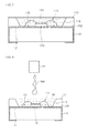
- a cavity 115 is formed in an upper portion 112 of a body 110.
- a plurality of lead electrodes 131 and 132 is disposed in the cavity 115.
- the light emitting diode 120 may include a colored LED such as a blue LED, a red LED, a green LED and/or an ultraviolet (UV) LED. Also, a plurality of LEDs may be disposed in the cavity 115. The plurality of LEDs may emit light having the same color or light having colors different from each other.
- a colored LED such as a blue LED, a red LED, a green LED and/or an ultraviolet (UV) LED.
- UV ultraviolet
- a plurality of LEDs may be disposed in the cavity 115. The plurality of LEDs may emit light having the same color or light having colors different from each other.
- the other ends of the lead electrodes 131 and 132 are exposed to the outside of the body 110 and may be used as external terminals.
- the light emitting diode 120 includes the blue LED
- phosphor for emitting yellow light may be added as the phosphor.
- Kinds of the light emitting diode 120 and the phosphor may be changed according to (or to obtain) a target light.
- the resin layer 150 to which the phosphor is added will be described in the following embodiments.
- the first layer 160 may be formed of a compound of a rubber material and a metal material.
- the rubber material may include silicon, an epoxy, and an acrylic material, and the metal (or a conductive) material may selectively include or contain C, Fe, Al, Ag, Au, Ti, Zn, and Sn.
- the metal material has color sensation such as a red-group color and a yellow-group color.
- a predetermined amount of an organic comprising material may be injected using a dispensing device 165 to form the first layer 160 on a top surface of the resin layer 150.
- the dispensing device 165 uses a PicoDot jet dispensing system, for example, but other injection or dispensing system or technique may be used.
- the organic comprising material 160A may be controlled to a dispensing amount in terms of a unit of a nanoliter per one dot.
- the dispensing amount controlled in terms of the nanoliter unit may finely change a thickness of the first layer 160.
- a thickness change of the first layer 160 containing a metal material having a color sensation may finely change a chromaticity coordinate distribution of light emitted through the resin layer 150 having a color sensation.
- the first layer 160 may have a thickness of about 50 ⁇ m or less.
- the first layer 160 may change a chromaticity coordinate distribution of light emitted from the light emitting diode 120 and the light emitted through the resin layer 150.
- the first layer 160 may shift the chromaticity coordinate distribution of the light emitted from the light emitting device 100 or the resin layer 150 to the chromaticity coordinates of the (or within) the target region.
- the light emitting diode 120 may use a rank out of a target rank, and the first layer 160 may shift a rank of the light emitting diode 120 to the chromaticity coordinate distribution of the target rank.
- the first layer 160 may be color-complementary to the chromaticity coordinates of the light emitted through the resin layer 150, or the first layer 160 and the resin layer 150 may have color distributions opposite to each other about the target region.
- the light emitting diode 120 may use the target rank and an available rank there around to improve utilization yield.
- the lens 170 adheres to a top surface of the first layer 160 to complete a package.
- the lens 170 may include a convex lens or a side emitting lens, but is not limited thereto.
- the lens 170 may improve orientation angles and brightness characteristics of the light emitting device 100.
- the lens 170 is formed of a resin material such as silicon or an epoxy. Since the lens 170 formed of the resin material does not have an adhesive property, a separate adhesion process using the first layer 160 may be performed to adhere the lens 170 to the body 110.
- the resin layer 150 is formed in the cavity 115 of the body 110.
- distribution of light emitted through the resin layer 150 may be measured to construct a color-sorting table according to light distribution characteristics of each of packages.
- a group out of the target rank may be designated using the color-sorting table, and then, a dotting amount of a organic comprising material corresponding to the designated group may be determined.
- Fig. 7 is a graph illustrating a wavelength change according to a dotting amount of a organic comprising material according to an embodiment of the invention.
- a wavelength abscises and a luminous intensity ordinate according to a dotting amount of a organic comprising material are finely changed.
- a light emitting diode emits light having a blue peak wavelength (450 nm)
- a phosphor emits yellow light (525 nm).
- the light emitted from the light emitting diode and the phosphor may be finely changed according to the dotting amount or a thickness of the organic comprising material.
- a chromaticity B rank of chromaticity A through E ranks of a light emitting device represents a target rank.
- the organic comprising material of about 20 dotting does not affect color, it may be set to a reference dotting amount.
- a chromaticity rank of a package may be changed to C, D, and E, respectively.
- the rank may be a region in which optical characteristics are subdivided based on chromaticity after the resin layer is formed.
- the resin layer is formed in the cavity 115.
- light distribution of each package is measured to construct a color-sorting table according to light distribution characteristics of the each of packages.
- groups i.e., C, D, and E
- a dotting amount of a organic comprising material corresponding to the designated group may be determined. That is, B, C, D, and E may dispense about 20 dotting amount, about 40 dotting amount, about 50 dotting amount, and about 60 dotting amount, respectively, to adjust a chromaticity rank of respective groups.
- Figs. 9 to 11 are graphs illustrating changes of light characteristics according to the number of dotting of a organic comprising material.
- Fig. 9 is a graph illustrating a change of a luminous intensity
- Fig. 10 is a graph illustrating a change of a chromaticity coordinate x
- Fig. 11 is a graph illustrating a change of a chromaticity coordinate y.
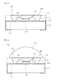
- Fig. 12 is a sectional view of a light emitting device according to another embodiment, and Fig. 13 is a partially enlarged view of Fig. 12 .
- the module board 210 includes a board 212 and a reflective layer 214.
- the board 212 may include a flexible PCB, a metal PCB, and a general PCB. Also, the board 212 may be used as bodies of the respective light emitting parts 200A.
- the reflective layer 214 may be integrally attached to the board 212 using a laminating or a pressing method.
- the module board 210 may serve as a body, but is not limited thereto.
- the cavity 213 may be defined on the reflective layer 214, but is not limited thereto.
- an optical sheet may be disposed on the module board 210, but is not limited thereto.
- a plurality of cavities 213 may be arrayed by a predetermined distance on the module board 210.
- the light emitting diode 220 may be electrically connected to a lead electrode disposed on the board 212.
- the light emitting diode 220 may be mounted using one of flip chip, die bonding, and wire bonding methods, but are not limited thereto.
- the cavities 213 of the module board 210 may be arrayed in at least one line by a predetermined distance. Alternately, a plurality of rows may be arrayed in a matrix shape or a zigzag shape, but is not limited thereto.
- a surface of the cavity 213 may have a circular shape or a polygonal shape, but is not limited thereto.
- the light emitting diode 220 disposed in the cavity 213 may include at least one of a colored LED such as a red LED, a green LED, a blue LED and/or an ultraviolet (UV) LED.
- a colored LED such as a red LED, a green LED, a blue LED and/or an ultraviolet (UV) LED.
- the resin layer 250 is disposed in the cavity 213.
- Phosphor may be added to a resin material such as silicon or an epoxy to form the resin layer 250.
- the phosphor may be selected in consideration of a relation between light of the light emitting diode 250 and target light.
- the light emitting module 200 may realize white light using a blue LED chip and a yellow LED chip or a dual LED chip.
- a top surface of the resin layer 250 may have a flat shape, a concave shape, or a convex shape, but is not limited thereto.
- the first layer 260 may be disposed on the resin layer 250.
- the first layer 260 may be formed of rubber materials (silicon or an acrylic material) and a compound of metals.
- the rubber materials may include silicon and an acrylic material, and the metals may selectively include C, Fe, Al, Ag, Au, Ti, Zn, and Sn.
- the metal material has a color sensation, such as a red-group color and a yellow-group color.
- the first layer 260 may be formed by dispensing the organic comprising material within a range of from about 20 dotting to about 60 dotting. Also, the organic comprising material may be controlled to a dispensing amount in terms of a unit of a nanoliter (e.g., 2 nanoliters) per one dot. The light distribution at each of the light emitting parts 200A may be changed to or within the target region by controlling a thickness of the first layer 260.
- the chromaticity coordinate distribution may be changed using the first layer 260.
- the utilization yield of the light emitting diode 220 may be improved.
- the lens 270 adheres to the resin layer 250 using the first layer 260.
- the lens 270 may include a convex lens or a side emitting lens, but is not limited thereto.
- an optical member may be disposed on the module board 210.
- the optical member may include a waveguide plate, an optical sheet, and/or a lens.
- the optical member may adhere to the resin layer 250 using the first layer 260.
- the chromaticity coordinate distribution may be moved to the target region using the first layer 260 having color sensation, and being disposed on the resin layer 250.
- the light emitting module 200 may be selectively applicable to a direct-view type light unit and a side-view type light unit. In addition, the light emitting module 200 may be applicable to portable terminals, various indication devices, and display devices.
- references to color sensation may refer to one of perceivable color, and may be one based on the CIE chromaticity coordinates, but is not limited thereto.
- a fabrication method of a light emitting device includes: disposing a light emitting diode on a body; forming a resin layer on the light emitting diode; forming a first layer containing a metal material on the resin layer; and attaching an optical member to the first layer.
- Embodiments of the invention may improve the utilization yield of the light emitting diode.
- Embodiments of the invention may improve the utilization yield of the package or module including the light emitting diode.
- the color distribution of the LED package or light emitting module may be moved (or shifted) to (or within) the target region.
- Embodiments of the invention may improve the utilization yield of the LED chip.
- Embodiments of the invention may improve the utilization yield of the LED package.
- Embodiments of the invention may improve the utilization yield of the light emitting module.
- any reference in this specification to "one embodiment,” “an embodiment,” “example embodiment,” etc. means that a particular feature, structure, or characteristic described in connection with the embodiment is included in at least one embodiment of the invention.
- the appearances of such phrases in various places in the specification are not necessarily all referring to the same embodiment.
Landscapes
- Led Device Packages (AREA)
- Non-Portable Lighting Devices Or Systems Thereof (AREA)
Applications Claiming Priority (1)
| Application Number | Priority Date | Filing Date | Title |
|---|---|---|---|
| KR1020090017732A KR101064005B1 (ko) | 2009-03-02 | 2009-03-02 | 발광 장치 및 그 제조방법 |
Publications (2)
| Publication Number | Publication Date |
|---|---|
| EP2226860A2 true EP2226860A2 (de) | 2010-09-08 |
| EP2226860A3 EP2226860A3 (de) | 2010-09-22 |
Family
ID=42262002
Family Applications (1)
| Application Number | Title | Priority Date | Filing Date |
|---|---|---|---|
| EP10154371A Withdrawn EP2226860A3 (de) | 2009-03-02 | 2010-02-23 | Lichtemittierende Vorrichtung |
Country Status (5)
| Country | Link |
|---|---|
| US (1) | US8860052B2 (de) |
| EP (1) | EP2226860A3 (de) |
| JP (1) | JP5697348B2 (de) |
| KR (1) | KR101064005B1 (de) |
| CN (1) | CN101826589B (de) |
Cited By (1)
| Publication number | Priority date | Publication date | Assignee | Title |
|---|---|---|---|---|
| GB2493796A (en) * | 2011-08-18 | 2013-02-20 | Alder Optomechanical Corp | Light emitting device |
Families Citing this family (8)
| Publication number | Priority date | Publication date | Assignee | Title |
|---|---|---|---|---|
| TW201020643A (en) * | 2008-11-25 | 2010-06-01 | Chi Mei Lighting Tech Corp | Side view type light-emitting diode package structure, and manufacturing method and application thereof |
| US8552438B2 (en) * | 2010-03-25 | 2013-10-08 | Micron Technology, Inc. | Multi-lens solid state lighting devices |
| CN102468407A (zh) * | 2010-11-17 | 2012-05-23 | 青岛杰生电气有限公司 | 一种紫外发光二极管 |
| JP5559027B2 (ja) * | 2010-12-24 | 2014-07-23 | 株式会社朝日ラバー | シリコーンレンズ、レンズ付led装置及びレンズ付led装置の製造方法 |
| CN102148297B (zh) * | 2010-12-28 | 2012-08-22 | 广州市鸿利光电股份有限公司 | 一种色光可均匀调配的led制造工艺及led |
| US8878215B2 (en) * | 2011-06-22 | 2014-11-04 | Lg Innotek Co., Ltd. | Light emitting device module |
| US20140014987A1 (en) * | 2012-07-10 | 2014-01-16 | Luminus Devices, Inc. | Methods and apparatuses for shifting chromaticity of light |
| DE102016204887A1 (de) * | 2016-03-23 | 2017-09-28 | E.G.O. Elektro-Gerätebau GmbH | Anzeigevorrichtung für ein Elektrogerät und Elektrogerät |
Citations (4)
| Publication number | Priority date | Publication date | Assignee | Title |
|---|---|---|---|---|
| JPH11145519A (ja) * | 1997-09-02 | 1999-05-28 | Toshiba Corp | 半導体発光素子、半導体発光装置および画像表示装置 |
| JP2005056885A (ja) * | 2003-08-04 | 2005-03-03 | Fine Rubber Kenkyusho:Kk | 半導体発光装置の製造方法 |
| US20060121371A1 (en) * | 2004-12-03 | 2006-06-08 | Innolux Display Corp. | Color filter having nanoparticles for liquid crystal display |
| JP2008235827A (ja) * | 2007-03-23 | 2008-10-02 | Matsushita Electric Works Ltd | 発光装置 |
Family Cites Families (15)
| Publication number | Priority date | Publication date | Assignee | Title |
|---|---|---|---|---|
| US6340824B1 (en) * | 1997-09-01 | 2002-01-22 | Kabushiki Kaisha Toshiba | Semiconductor light emitting device including a fluorescent material |
| JP3614776B2 (ja) * | 2000-12-19 | 2005-01-26 | シャープ株式会社 | チップ部品型ledとその製造方法 |
| JP2003152227A (ja) | 2001-11-14 | 2003-05-23 | Citizen Electronics Co Ltd | Ledの色補正手段および色補正方法 |
| US6734465B1 (en) * | 2001-11-19 | 2004-05-11 | Nanocrystals Technology Lp | Nanocrystalline based phosphors and photonic structures for solid state lighting |
| JP2004031003A (ja) | 2002-06-24 | 2004-01-29 | Mitsuboshi Belting Ltd | ランプバルブ用着色剤及びアンバー色を呈するランプバルブ |
| JP4280050B2 (ja) | 2002-10-07 | 2009-06-17 | シチズン電子株式会社 | 白色発光装置 |
| WO2006059828A1 (en) | 2004-09-10 | 2006-06-08 | Seoul Semiconductor Co., Ltd. | Light emitting diode package having multiple molding resins |
| US7670872B2 (en) * | 2004-10-29 | 2010-03-02 | LED Engin, Inc. (Cayman) | Method of manufacturing ceramic LED packages |
| JP4591106B2 (ja) | 2005-02-10 | 2010-12-01 | パナソニック電工株式会社 | 白色発光装置 |
| EP2280430B1 (de) * | 2005-03-11 | 2020-01-01 | Seoul Semiconductor Co., Ltd. | LED-Kapselung mit einer Gruppe in Reihe geschalteter Leuchtzellen |
| US7329907B2 (en) * | 2005-08-12 | 2008-02-12 | Avago Technologies, Ecbu Ip Pte Ltd | Phosphor-converted LED devices having improved light distribution uniformity |
| CN101253637A (zh) | 2005-08-30 | 2008-08-27 | 奥斯兰姆奥普托半导体有限责任公司 | 光电子器件 |
| JP2007173547A (ja) | 2005-12-22 | 2007-07-05 | Toshiba Lighting & Technology Corp | 発光装置 |
| WO2007125493A2 (en) | 2006-05-02 | 2007-11-08 | Koninklijke Philips Electronics N.V. | Color-stable phosphor converted led |
| US20070269586A1 (en) * | 2006-05-17 | 2007-11-22 | 3M Innovative Properties Company | Method of making light emitting device with silicon-containing composition |
-
2009
- 2009-03-02 KR KR1020090017732A patent/KR101064005B1/ko not_active Expired - Fee Related
- 2009-12-28 US US12/648,118 patent/US8860052B2/en active Active
-
2010
- 2010-02-23 EP EP10154371A patent/EP2226860A3/de not_active Withdrawn
- 2010-02-25 CN CN201010125218.1A patent/CN101826589B/zh not_active Expired - Fee Related
- 2010-03-02 JP JP2010045212A patent/JP5697348B2/ja not_active Expired - Fee Related
Patent Citations (4)
| Publication number | Priority date | Publication date | Assignee | Title |
|---|---|---|---|---|
| JPH11145519A (ja) * | 1997-09-02 | 1999-05-28 | Toshiba Corp | 半導体発光素子、半導体発光装置および画像表示装置 |
| JP2005056885A (ja) * | 2003-08-04 | 2005-03-03 | Fine Rubber Kenkyusho:Kk | 半導体発光装置の製造方法 |
| US20060121371A1 (en) * | 2004-12-03 | 2006-06-08 | Innolux Display Corp. | Color filter having nanoparticles for liquid crystal display |
| JP2008235827A (ja) * | 2007-03-23 | 2008-10-02 | Matsushita Electric Works Ltd | 発光装置 |
Cited By (1)
| Publication number | Priority date | Publication date | Assignee | Title |
|---|---|---|---|---|
| GB2493796A (en) * | 2011-08-18 | 2013-02-20 | Alder Optomechanical Corp | Light emitting device |
Also Published As
| Publication number | Publication date |
|---|---|
| JP2010206206A (ja) | 2010-09-16 |
| KR101064005B1 (ko) | 2011-09-08 |
| US8860052B2 (en) | 2014-10-14 |
| KR20100098988A (ko) | 2010-09-10 |
| JP5697348B2 (ja) | 2015-04-08 |
| US20100219435A1 (en) | 2010-09-02 |
| EP2226860A3 (de) | 2010-09-22 |
| CN101826589B (zh) | 2016-02-03 |
| CN101826589A (zh) | 2010-09-08 |
Similar Documents
| Publication | Publication Date | Title |
|---|---|---|
| US8860052B2 (en) | Light emitting device | |
| TWI474468B (zh) | 發光模組及具有發光模組之顯示裝置 | |
| KR101208174B1 (ko) | 광학시트 및 이를 포함하는 발광소자패키지 | |
| US9564567B2 (en) | Light emitting device package and method of fabricating the same | |
| CN105355764B (zh) | 发光装置 | |
| US20080007939A1 (en) | Direct-type backlight unit having surface light source | |
| EP2400569B1 (de) | Verpackung für lichtemittierende Diode | |
| US8282229B2 (en) | Light emitting module, backlight unit, and display apparatus | |
| EP2312656A2 (de) | Lichtemittierende Vorrichtung und Beleuchtungssystem | |
| US20110198628A1 (en) | Multi-chip led package | |
| US8896016B2 (en) | LED lighting module and method of making the same | |
| US8476662B2 (en) | Light emitting device, method for manufacturing the same, and backlight unit | |
| CN212725360U (zh) | 一种led发光件 | |
| KR100702569B1 (ko) | 반사면 부착형 발광소자 | |
| KR20130017689A (ko) | 발광소자 어레이 | |
| KR101693656B1 (ko) | 백라이트 유닛 및 이를 포함하는 디스플레이 장치 | |
| US11581460B2 (en) | Light emitting module and method for manufacturing light emitting module | |
| KR20120087581A (ko) | 발광소자 패키지 | |
| KR20110091222A (ko) | 발광 다이오드 모듈 |
Legal Events
| Date | Code | Title | Description |
|---|---|---|---|
| PUAI | Public reference made under article 153(3) epc to a published international application that has entered the european phase |
Free format text: ORIGINAL CODE: 0009012 |
|
| PUAL | Search report despatched |
Free format text: ORIGINAL CODE: 0009013 |
|
| 17P | Request for examination filed |
Effective date: 20100223 |
|
| AK | Designated contracting states |
Kind code of ref document: A2 Designated state(s): AT BE BG CH CY CZ DE DK EE ES FI FR GB GR HR HU IE IS IT LI LT LU LV MC MK MT NL NO PL PT RO SE SI SK SM TR |
|
| AX | Request for extension of the european patent |
Extension state: AL BA RS |
|
| AK | Designated contracting states |
Kind code of ref document: A3 Designated state(s): AT BE BG CH CY CZ DE DK EE ES FI FR GB GR HR HU IE IS IT LI LT LU LV MC MK MT NL NO PL PT RO SE SI SK SM TR |
|
| AX | Request for extension of the european patent |
Extension state: AL BA RS |
|
| RAP1 | Party data changed (applicant data changed or rights of an application transferred) |
Owner name: LG INNOTEK CO., LTD. |
|
| 17Q | First examination report despatched |
Effective date: 20110921 |
|
| RAP1 | Party data changed (applicant data changed or rights of an application transferred) |
Owner name: LG INNOTEK CO., LTD. |
|
| STAA | Information on the status of an ep patent application or granted ep patent |
Free format text: STATUS: THE APPLICATION IS DEEMED TO BE WITHDRAWN |
|
| 18D | Application deemed to be withdrawn |
Effective date: 20160531 |