EP2230208B1 - Form für Galvanoplastik und ihr Herstellungsverfahren - Google Patents
Form für Galvanoplastik und ihr Herstellungsverfahren Download PDFInfo
- Publication number
- EP2230208B1 EP2230208B1 EP20100154909 EP10154909A EP2230208B1 EP 2230208 B1 EP2230208 B1 EP 2230208B1 EP 20100154909 EP20100154909 EP 20100154909 EP 10154909 A EP10154909 A EP 10154909A EP 2230208 B1 EP2230208 B1 EP 2230208B1
- Authority
- EP
- European Patent Office
- Prior art keywords
- cavity
- layer
- mould
- electrically insulating
- recess
- Prior art date
- Legal status (The legal status is an assumption and is not a legal conclusion. Google has not performed a legal analysis and makes no representation as to the accuracy of the status listed.)
- Active
Links
Images


Classifications
-
- C—CHEMISTRY; METALLURGY
- C25—ELECTROLYTIC OR ELECTROPHORETIC PROCESSES; APPARATUS THEREFOR
- C25D—PROCESSES FOR THE ELECTROLYTIC OR ELECTROPHORETIC PRODUCTION OF COATINGS; ELECTROFORMING; APPARATUS THEREFOR
- C25D1/00—Electroforming
- C25D1/10—Moulds; Masks; Masterforms
-
- B—PERFORMING OPERATIONS; TRANSPORTING
- B81—MICROSTRUCTURAL TECHNOLOGY
- B81C—PROCESSES OR APPARATUS SPECIALLY ADAPTED FOR THE MANUFACTURE OR TREATMENT OF MICROSTRUCTURAL DEVICES OR SYSTEMS
- B81C99/00—Subject matter not provided for in other groups of this subclass
- B81C99/0075—Manufacture of substrate-free structures
- B81C99/009—Manufacturing the stamps or the moulds
-
- C—CHEMISTRY; METALLURGY
- C25—ELECTROLYTIC OR ELECTROPHORETIC PROCESSES; APPARATUS THEREFOR
- C25D—PROCESSES FOR THE ELECTROLYTIC OR ELECTROPHORETIC PRODUCTION OF COATINGS; ELECTROFORMING; APPARATUS THEREFOR
- C25D17/00—Constructional parts, or assemblies thereof, of cells for electrolytic coating
-
- B—PERFORMING OPERATIONS; TRANSPORTING
- B81—MICROSTRUCTURAL TECHNOLOGY
- B81B—MICROSTRUCTURAL DEVICES OR SYSTEMS, e.g. MICROMECHANICAL DEVICES
- B81B2201/00—Specific applications of microelectromechanical systems
- B81B2201/03—Microengines and actuators
- B81B2201/035—Microgears
Definitions
- the invention relates to a mold for manufacturing a micromechanical part by electroplating and its manufacturing process.
- LIGA-type processes (well-known abbreviation from German “RöntgenLithographie, Galvanoformung &Abforrnung”) are more recent. They consist in forming a mold by photolithography of a photosensitive resin and then electroplating a metal deposit such as nickel. The accuracy of such LIGA processes is much better than that of a conventional mold obtained, for example, by machining. Such accuracies thus allow the manufacture of micromechanical parts, especially for watch movements that were previously unthinkable (see, for example, EP Patent 1681375 and EP 0547371 ).
- the purpose of the present invention is to overcome all or part of the disadvantages mentioned above by proposing an alternative mold offering at least the same manufacturing precisions and authorizing the manufacture of multi-level and / or large-pitched parts.
- the invention relates to a mold intended to manufacture a micromechanical part by electroplating, characterized in that it comprises a substrate comprising a top layer and a lower layer of crystalline silicon doped electrically conductive and secured together by a layer electrically insulating intermediate, the upper layer having at least one cavity revealing a portion of the lower layer of said substrate and having electrically insulating walls for growing an electrolytic deposit in said at least one cavity.
- the invention relates to a method of manufacturing a micromechanical part 41, 41 ', 41 "by electroplating, method 1 preferably comprises a method of manufacturing a mold 39, 39', 39 "Follow the steps of electroplating 5 and release 7 of the part 41, 41 ', 41" of said mold.
- the manufacturing process 3 of the mold comprises successive steps for manufacturing a mold 39, 39 ', 39 "preferably comprising silicon-based materials.
- a first step 10 of the method 3 consists in providing a substrate 9, 9 'comprising an upper layer 21, 21' and a lower layer 23, 23 'made of electrically micro-machinable materials. conductors, secured together by an intermediate layer 22, 22 'electrically insulating as illustrated in FIGS. figures 1 and 8 .
- the substrate 9, 9 ' is a S.O.I. (Well known abbreviation from the English term "Silicon On Isulator").
- the upper layers 21, 21 'and lower 23, 23' are sufficiently doped crystalline silicon to be electrically conductive and the intermediate layer of silicon dioxide.
- the method 3 comprises two distinct embodiments from the step 11 respectively represented by a triple line and a single line to the figure 13 .
- a mask 15 and then a protective mask 24 are structured on the upper conductive layer 21 as illustrated in FIG. figure 2 .
- the mask 15 comprises at least one pattern 27 which does not cover the upper layer 21.
- the mask 24, which completely covers the mask 15 comprises at least one pattern 26 which does not cover the upper layer 21.
- the mask 15 may be made by depositing a silicon oxide layer to form said mask to a predetermined height. Then, the mask 24 may, for example, be obtained by photolithography using a photoresist covering the mask 15.
- the upper layer 21 is etched until the intermediate layer 22 is discovered.
- the etching step 2 preferably comprises an anisotropic dry attack of the deep reactive ion etching type ( DRIE from the English term "Deep Reactive Ion Etching").
- a first step of step 2 an anisotropic etching is carried out in the upper layer 21 according to the pattern 26 of the mask 24. This etching makes it possible to start the etching of at least one cavity 25 in the upper layer 21 on a part of its thickness.
- a second step the mask 24 is removed and then a second anisotropic etching is carried out according to the pattern 27 of the mask 15 still present on the upper layer 21. The second etching makes it possible to continue the etching of said at least one cavity 25, but also of begin etching at least one recess 28 which communicates with said at least one cavity 25 while being of larger section.
- a fourth step 4 the mask 15 is removed. So, as visible at the figure 3 at the end of the fourth step 4, the upper layer 21 is etched throughout its thickness of said at least one cavity 25 and on an upper part of its thickness of said at least one recess 28.
- an electrically insulating coating 30 is deposited by covering the upper assembly of the substrate 9 as illustrated in FIG. figure 4 .
- the coating 30 is obtained by oxidation of the top of the etched upper layer 21 and the intermediate layer 22.
- Step 8 a directional etching of the coating 30 and the intermediate layer 22 is performed.
- Step 8 is intended to limit the presence of insulating layers only at each vertical wall formed in the upper layer 21, that is to say the walls 31 and 32 respectively of said at least one cavity 25 and said least one recess 28.
- the vertical component of the etching phenomenon is favored with respect to the horizontal composition, by modulating, for example, the pressure in the chamber (pressure work very low), in a RIE reactor.
- Such an engraving may, for example, be of the "ion milling" or "sputter etching” type.
- step 8 the bottom of the cavity 25 discovers the lower layer 23 electrically conductive and the bottom of the recess 28 discovers the upper layer 21 also conductive.
- an attachment layer on the bottom of each cavity 25 and / or on the bottom of each recess 28 may be provided.
- the bonding layer could then consist of a metal such as CrAu alloy.
- a rod 29 is mounted to directly form the axis hole 42 of the micromechanical part 41 during electroplating step 5.
- This has the advantage not only of not having to machine part 41 after electroplating is completed but also to be able to make any shape of inner section, uniformly or otherwise, over the entire height of hole 42.
- the rod 29 is obtained, for example, using a photolithography process of a photosensitive resin.
- step 8 the manufacturing process 3 of the mold 39 is finished and the manufacturing process 1 of the micromechanical part continues with the electroplating and release 7 steps of FIG. the piece 41 of the mold 39.
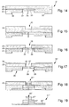
- the electroplating step 5 is carried out by connecting the deposition electrode to the lower layer 23 of the mold 39 so as to firstly grow an electrolytic deposit in the cavity 25 of said mold and then, only in a second step, in the 'recess 28 as illustrated in the figure 6 .
- the electrolytic deposit when it is flush with the upper part of the cavity 25, it electrically connects the upper layer 21 by, optionally, its attachment layer, which allows the continuation of the growth of the deposit sure the assembly of the recess 28.
- the invention allows the production of parts 41 with great slenderness, that is to say when the section of the cavity 25 is much smaller than that of the recess 28, avoiding the problems of delamination even with a nickel-phosphorus material at, for example, 12% phosphorus.
- the manufacturing method 1 ends with step 7, in which the part 41 formed in the cavity 25 and then in the recess 28 is released from the mold 39.
- the release step 7 can, for example, be performed by etching layers 23 and 21.
- the micromechanical part 41 obtained has two levels 43, 45 of different shape each in a perfectly independent thickness and having a single pin hole 42.
- Such a micromechanical part 41 could, for example, be a coaxial escapement wheel or an escape wheel assembly 43 - pinion 45 having a geometrical precision of the order of a micrometer but also an ideal referencing that is to say to say a perfect positioning between said levels.
- the method 3 comprises a second step 11, consisting of structuring at least one mask 24 'of protection on the upper conductive layer 21' as illustrated in FIG. figure 8 .
- the mask 24 ' has at least one pattern 26' which does not cover the upper layer 21 '.
- Such a mask 24 'can for example, be obtained by photolithography using a photoresist.
- the upper layer 21 ' is etched until discovering the intermediate layer 22'.
- the etching step 12 preferably comprises an anisotropic dry etching of the deep reactive ion etching (DRIE) type. The anisotropic etching is performed in the upper layer 21 'according to the pattern 26' of the mask 24 '.
- DRIE deep reactive ion etching
- a fourth step 14 the mask 24 'is removed. So, as visible at the figure 9 at the end of the fourth step 14, the upper layer 21 'is etched throughout its thickness of at least one cavity 25'.
- an electrically insulating coating 30 ' is deposited by covering the upper assembly of the substrate 9' as illustrated in FIG. figure 10 .
- the coating 30 ' is obtained by oxidation of the top of the upper layer 21' etched and the intermediate layer 22 '.
- Step 18 a directional etching of the coating 30 'and the intermediate layer 22' is carried out.
- Step 18 is intended to limit the presence of insulating layers only at each vertical wall formed in the upper layer 21 ', that is to say the walls 31' of said at least one cavity 25 '.
- an attachment layer on the bottom of each cavity 25 'and / or on the top of the upper layer 21' may be provided.
- the bonding layer could then consist of a metal such as CrAu alloy.
- a rod can be mounted to form directly the axis hole of the micromechanical part during electroplating step 5 with the same advantages as mentioned above.
- step 18 the manufacturing method 3 of the mold 39 'is finished and the manufacturing process 1 of the micromechanical part continues with the electroplating and release steps 7 of the mold part 39 '.
- Step 5 of electroplating is performed by connecting the deposition electrode to the lower layer 23 'of the mold 39' in order to grow an electrolytic deposit in the cavity 25 'of the mold 39'.
- the manufacturing method 1 ends with the step 7 similar to that explained in the first embodiment, in which the piece formed in the cavity 25 'is released from the mold 39'.
- the micromechanical part obtained has a single level of identical shape over its entire thickness and may include an axis hole.
- Such a micromechanical part could, for example, be an escape wheel or an escapement anchor or even a pinion having a geometric precision of the order of a micrometer.
- the manufacturing method 3 of the mold 39 ' has a further step 20 for forming at least a second level of the mold 39' as illustrated in FIG. figure 12 .
- the second level is achieved by mounting a piece 27 ', having walls 32' electrically insulating, on the upper layer 21 'which has not been removed in step 12.
- the added piece 27 ' forms at least one recess 28' of larger section than the removed portions 25 ', for example, using a photolithography process of a photoresist.
- Exhibit 27 'could also include a insulating silicon material previously etched and then secured to the conductive layer 21 '.
- step 20 the manufacturing method 3 of the mold 39 'is completed and the manufacturing process 1 of the micromechanical part continues with the steps of electroplating 5 and release 7 of the piece 41 'of the mold 39'.
- the electroplating step 5 is carried out by connecting the deposition electrode to the lower layer 23 'of the mold 39' so as to initially grow an electrolytic deposit in the cavity 25 'of said mold, and then only in a second step in the recess 28 'as illustrated in FIG. figure 12 .
- the electrolytic deposit when it is flush with the upper part of the cavity 25 ', it electrically connects the top layer 21' with, optionally, its attachment layer, which allows the continuation of the growth. depositing on the entire recess 28 '.
- the invention allows the production of parts 41 'with great slenderness, that is to say when the section of the cavity 25' is much smaller than that of the recess 28 ', avoiding the problems of delamination even with a nickel-phosphorus material at, for example, 12% phosphorus.
- the manufacturing method 1 ends in step 7 similar to that explained in the first embodiment, in which the piece 41 'formed in the mold 39' is released.
- the micromechanical part 41 'obtained has two levels of shape each different to a perfectly independent thickness and may include a single pinhole.
- Such a micromechanical part 41 'can consequently have the same shape as that obtained by the first embodiment and thus include a geometrical precision of the order of a micrometer but also an ideal referencing, that is to say a positioning perfect between said levels.
- the variant remains identical to method 1 described above until step 8, 18 or 20 according to the embodiment used.
- the starting point of method 1 will be the example of the first embodiment as illustrated in FIG. figure 13 in triple line.
- the lower layer 23 is intended to be etched in order to form at least one second cavity 35 in the mold 39 ".
- a deposit 33 has been made in a portion of the first cavity 25 to provide an electroplating starting layer.
- this deposit 33 is carried out starting from step 5 to a predetermined thickness.
- this deposit can be carried out according to another method.
- variant of method 1 applies to the lower layer 23, steps 11, 12, 14, 16 and 18 of the second embodiment of method 3.
- the method 3 comprises a new step 11, consisting of structuring at least one mask 34 on the lower conductive layer 23 as illustrated in FIG. figure 15 .
- the mask 34 comprises at least one pattern 36 which does not cover the lower layer 23.
- Such a mask 34 may, for example, be obtained by photolithography using a photoresist.
- the layer 23 is etched according to the pattern 36 until the electrically conductive deposit 33 is discovered. Then the protective mask 34 is removed in a new step 14. Thus, as visible in FIG. figure 16 at the end of step 14, the bottom layer 23 is etched over its entire thickness with at least one cavity 35.
- an electrically insulating coating 38 is deposited by covering the bottom assembly of the substrate 9 "as shown in FIG. figure 17 .
- the coating 38 is obtained by depositing a silicon oxide on the top of the lower layer 23, for example, using a physical vapor deposition.
- a new step 18 is not necessary if only one level is added to the mold 39. Otherwise, a directional etching of the coating 38 is performed
- the new step 18 would be intended to limit the presence of insulating layer only at the level of each vertical wall 39 formed in the lower layer 23, that is to say the walls of said at least one cavity 35.
- a new step 18 is performed only to remove the oxide layer present in the bottom of the at least one cavity 35.
- a rod 37 can be mounted to directly form the hole 42 "axis of the micromechanical part 41" during the electroplating step 5 with the same advantages as mentioned above. .
- the manufacturing method 3 of the mold 39 is finished and the manufacturing process 1 of the micromechanical part continues with the electroplating and release steps 7 preferably, if the rods 29 and 37 are respectively formed in the cavities 25 and 35, they are preferably aligned, preferably the rod 37 is obtained, for example, using a photolithography process of a photosensitive resin.
- the electroplating step 5 is performed by connecting the deposition electrode to the lower layer 23 in order to grow an electrolytic deposit in the cavity 35 and also to continue the growth of the deposit in the cavity 25, then, only in a second step, in the recess 28 as illustrated in FIG. figure 18 .
- the manufacturing method 1 ends with step 7, in which the part 41 "is released from the mold 39" as explained above.
- the micromechanical part 41 "obtained has at least three levels 43", 45 “and 47” of different shape each in a perfectly independent thickness with a single axis hole 42 ".
- Such a micromechanical part could, for example, be a coaxial escape wheel 43 “, 45” with its pinion 47 “or a mobile with three levels of teeth 43", 45 “, 47” having a geometric precision of the micrometer order but also an ideal referencing that is to say a perfect positioning between said levels.
Landscapes
- Engineering & Computer Science (AREA)
- Chemical & Material Sciences (AREA)
- Chemical Kinetics & Catalysis (AREA)
- Electrochemistry (AREA)
- Materials Engineering (AREA)
- Metallurgy (AREA)
- Organic Chemistry (AREA)
- Manufacturing & Machinery (AREA)
- Microelectronics & Electronic Packaging (AREA)
- Micromachines (AREA)
- ing And Chemical Polishing (AREA)
- Moulds For Moulding Plastics Or The Like (AREA)
Claims (17)
- Verfahren (3) zum Herstellen einer Form (39, 39', 39"), das die folgenden Schritte umfasst:a) Vorsehen (10) eines Substrats (9, 9'), das eine obere Schicht (21, 21') und eine untere Schicht (23, 23') aus kristallinem Silicium, das mit einem elektrischen Leiter dotiert ist, die durch eine elektrisch isolierende Zwischenschicht (22, 22') miteinander verbunden sind, enthält;b) Ätzen (11, 12, 14, 2, 4) wenigstens eines Musters (26, 26', 27) in der oberen Schicht (21, 21') bis zu der Zwischenschicht (22, 22'), um wenigstens einen Hohlraum (25, 25') der Form zu bilden;c) Abdecken (6, 16) des oberen Teils des Substrats mit einer elektrisch isolierenden Beschichtung (30, 30');d) Ätzen (8, 18) auf gerichtete Weise der Beschichtung und der Zwischenschicht, um ihr Vorhandensein ausschließlich auf die Höhe jeder vertikalen Wand (31, 31', 33), die in der oberen Schicht gebildet ist, einzuschränken.
- Verfahren (3) nach Anspruch 1, dadurch gekennzeichnet, dass im Schritt b) ein zweites Muster (27) geätzt wird, um wenigstens eine Aussparung (28) zu bilden, die mit dem wenigstens einen Hohlraum kommuniziert und für die obere Schicht eine zweite Höhe bietet.
- Verfahren (3) nach Anspruch 1, dadurch gekennzeichnet, dass nach dem Schritt d) ein Teil (27') montiert wird, um wenigstens eine Aussparung (28') zu bilden, die mit dem wenigstens einen Hohlraum kommuniziert und für die Form eine zweite Höhe bietet.
- Verfahren (3) nach einem der vorhergehenden Ansprüche, dadurch gekennzeichnet, dass es den folgenden letzten Schritt umfasst:e) Bilden (8, 18) eines Stifts (29, 29') durch Photolithographie in dem wenigstens einen Hohlraum, um in dem künftigen Teil (41, 41'), das in der Form verwirklicht wird, ein Loch (42, 42') zu bilden.
- Verfahren (3) nach einem der vorhergehenden Ansprüche, dadurch gekennzeichnet, dass es nach den vorhergehenden Schritten die folgenden Schritte umfasst:a') Ablagern eines elektrisch leitenden Materials auf dem Boden des wenigstens einen Hohlraums;b') Ätzen (11, 12, 14, 2, 4) eines Musters (26, 26', 27) in der unteren Schicht (23, 23') bis zu der Ablagerung (33) des leitenden Materials, um wenigstens einen Hohlraum (35) der Form zu bilden;c') Abdecken (6, 16) der Gesamtheit mit einer zweiten elektrisch isolierenden Abdeckung (38).
- Verfahren (3) nach Anspruch 5, dadurch gekennzeichnet, dass es nach dem Schritt c') den folgenden Schritt umfasst:d') Ätzen (8, 18) auf gerichtete Weise der zweiten Beschichtung, um ihr Vorhandensein ausschließlich auf Höhe jeder vertikalen Wand (39), die in der unteren Schicht gebildet ist, einzuschränken.
- Verfahren (3) nach Anspruch 6, dadurch gekennzeichnet, dass im Schritt b') ein zweites Muster geätzt wird, um wenigstens eine Aussparung zu bilden, die mit dem wenigstens einen Hohlraum kommuniziert und für die untere Schicht eine zweite Höhe bietet.
- Verfahren (3) nach Anspruch 6, dadurch gekennzeichnet, dass nach dem Schritt d') ein Teil montiert wird, um wenigstens eine Aussparung zu bilden, die mit dem wenigstens einen Hohlraum kommuniziert und für die Form eine zweite Höhe bietet.
- Verfahren (3) nach einem der Ansprüche 5 bis 8, dadurch gekennzeichnet, dass es den folgenden letzten Schritt umfasst:e') Bilden eines Stifts (37) durch Photolithographie in dem wenigstens einen Hohlraum der unteren Schicht (23, 23'), um in dem künftigen Teil (41"), das in der Form verwirklicht wird, ein Loch (42") zu bilden.
- Verfahren (3) nach einem der vorhergehenden Ansprüche, dadurch gekennzeichnet, dass auf demselben Substrat (9, 9', 9") mehrere Formen (39, 39', 39") hergestellt werden.
- Verfahren (3) nach einem der vorhergehenden Ansprüche, dadurch gekennzeichnet, dass der Schritt c) durch Oxidation des oberen Teils des Substrats erhalten wird.
- Verfahren (3) nach dem vorhergehenden Anspruch, dadurch gekennzeichnet, dass die elektrisch isolierende Beschichtung (30, 30') durch Siliciumdioxid gebildet wird.
- Herstellungsverfahren (1) durch Galvanoplastie eines mikromechanischen Teils (41, 41', 41 "), dadurch gekennzeichnet, dass es die folgenden Schritte umfasst:i) Herstellen einer Form (39, 39', 39") gemäß dem Verfahren (3) nach einem der vorhergehenden Ansprüche;j) Verwirklichen (5) einer Elektroabscheidung durch Verbinden der Elektrode mit der unteren leitenden Schicht (23, 23') des Substrats (9, 9', 9"), um das Teil in der Form zu bilden;k) Freigeben des Teils (41, 41', 41 ") von der Form.
- Form (39, 39', 39"), die für die Herstellung eines mikromechanischen Teils (41, 41', 41") durch Galvanoplastie bestimmt ist, dadurch gekennzeichnet, dass sie ein Substrat (9, 9', 9") umfasst, das eine obere Schicht (21, 21') und eine untere Schicht (23, 23') aus kristallinem Silicium, das mit einem elektrischen Leiter dotiert ist, die durch eine elektrisch isolierende Zwischenschicht (22, 22') miteinander verbunden sind, enthält, wobei die obere Schicht (21, 21') wenigstens einen Hohlraum (25, 25') umfasst, der einen Teil der unteren Schicht (23, 23') des Substrats abdeckt und elektrisch isolierende Wände (31, 31') aus Siliciumdioxid aufweist, die ermöglichen, eine elektrolytische Ablagerung in dem wenigstens einen Hohlraum aufwachsen zu lassen.
- Form (39, 39', 39") nach Anspruch 14, dadurch gekennzeichnet, dass die obere Schicht (21, 21') außerdem wenigstens eine Aussparung (28, 28') aufweist, die so angeordnet ist, dass sie mit dem wenigstens einen Hohlraum kommuniziert, und elektrisch isolierende Wände (32, 32') aufweist, die ermöglichen, die elektrolytische Ablagerung in der wenigstens einen Aussparung fortzusetzen, nachdem der wenigstens eine Hohlraum gefüllt worden ist.
- Form (39") nach Anspruch 14 oder 15, dadurch gekennzeichnet, dass die untere Schicht (23, 23') wenigstens einen Hohlraum (35) umfasst, der einen Teil der elektrisch leitenden Schicht (33) des Substrats abdeckt und elektrisch isolierende Wände (40) aus Siliciumdioxid aufweist, die ermöglichen, eine elektrolytische Ablagerung in dem wenigstens einen Hohlraum der unteren Schicht (23, 23') aufwachsen zu lassen.
- Form nach Anspruch 16, dadurch gekennzeichnet, dass die untere Schicht (23, 23') außerdem wenigstens eine Aussparung umfasst, die so angeordnet ist, dass sie mit dem wenigstens einen Hohlraum der unteren Schicht (23, 23') kommuniziert, und elektrisch isolierende Wände aufweist, die ermöglichen, die elektrolytische Ablagerung in der wenigstens einen Aussparung fortzusetzen, nachdem der wenigstens eine Hohlraum der unteren Schicht (23, 23') gefüllt worden ist.
Priority Applications (1)
| Application Number | Priority Date | Filing Date | Title |
|---|---|---|---|
| EP20100154909 EP2230208B1 (de) | 2009-03-13 | 2010-02-26 | Form für Galvanoplastik und ihr Herstellungsverfahren |
Applications Claiming Priority (2)
| Application Number | Priority Date | Filing Date | Title |
|---|---|---|---|
| EP20090155125 EP2230207A1 (de) | 2009-03-13 | 2009-03-13 | Form für Galvanoplastik und ihr Herstellungsverfahren |
| EP20100154909 EP2230208B1 (de) | 2009-03-13 | 2010-02-26 | Form für Galvanoplastik und ihr Herstellungsverfahren |
Publications (2)
| Publication Number | Publication Date |
|---|---|
| EP2230208A1 EP2230208A1 (de) | 2010-09-22 |
| EP2230208B1 true EP2230208B1 (de) | 2014-01-08 |
Family
ID=41047360
Family Applications (2)
| Application Number | Title | Priority Date | Filing Date |
|---|---|---|---|
| EP20090155125 Withdrawn EP2230207A1 (de) | 2009-03-13 | 2009-03-13 | Form für Galvanoplastik und ihr Herstellungsverfahren |
| EP20100154909 Active EP2230208B1 (de) | 2009-03-13 | 2010-02-26 | Form für Galvanoplastik und ihr Herstellungsverfahren |
Family Applications Before (1)
| Application Number | Title | Priority Date | Filing Date |
|---|---|---|---|
| EP20090155125 Withdrawn EP2230207A1 (de) | 2009-03-13 | 2009-03-13 | Form für Galvanoplastik und ihr Herstellungsverfahren |
Country Status (7)
| Country | Link |
|---|---|
| US (2) | US8512539B2 (de) |
| EP (2) | EP2230207A1 (de) |
| JP (1) | JP5443220B2 (de) |
| KR (1) | KR20100103434A (de) |
| CN (1) | CN101831672B (de) |
| RU (1) | RU2526108C2 (de) |
| TW (1) | TWI598206B (de) |
Families Citing this family (15)
| Publication number | Priority date | Publication date | Assignee | Title |
|---|---|---|---|---|
| EP2230206B1 (de) * | 2009-03-13 | 2013-07-17 | Nivarox-FAR S.A. | Form für Galvanoplastik und ihr Herstellungsverfahren |
| EP2263971A1 (de) * | 2009-06-09 | 2010-12-22 | Nivarox-FAR S.A. | Mikromechanisches Verbundbauteil und sein Herstellungsverfahren |
| JP5773624B2 (ja) * | 2010-01-08 | 2015-09-02 | キヤノン株式会社 | 微細構造体の製造方法 |
| WO2012084047A1 (en) * | 2010-12-23 | 2012-06-28 | Replisaurus Group Sas | An ecpr master electrode and a method for providing such ecpr master electrode |
| CN102167282A (zh) * | 2011-04-07 | 2011-08-31 | 天津海鸥表业集团有限公司 | 一种硅与金属复合材料的微结构加工方法 |
| KR101351221B1 (ko) * | 2011-09-21 | 2014-01-14 | 한국전력공사 | 테이프 캐스팅을 이용한 지지체식 코팅막의 제조방법 |
| WO2013072955A1 (ja) * | 2011-11-15 | 2013-05-23 | 株式会社Leap | 多段転写金型の製造方法、その多段転写金型、及びそれによる部品 |
| EP2767869A1 (de) * | 2013-02-13 | 2014-08-20 | Nivarox-FAR S.A. | Verfahren zur Herstellung eines mikromechanischen Monoblock-Bauteils, das mindestens zwei verschiedene Ebenen umfasst |
| CH708827A2 (fr) * | 2013-11-08 | 2015-05-15 | Nivarox Sa | Pièce de micromécanique creuse, à plusieurs niveaux fonctionnels et monobloc en un matériau à base d'un allotrope synthétique du carbone. |
| CH710107B1 (fr) * | 2014-09-09 | 2019-06-14 | Seiko Instr Lnc | Composant mécanique, mouvement, pièce d'horlogerie et méthode de fabrication du composant mécanique. |
| EP3109199B1 (de) * | 2015-06-25 | 2022-05-11 | Nivarox-FAR S.A. | Werkstück auf siliziumbasis mit mindestens einer fase, und sein herstellungsverfahren |
| CN105729683B (zh) * | 2016-03-18 | 2017-12-01 | 宁波双林模具有限公司 | 一种注塑模具型腔精密仿真皮纹型面的制作方法 |
| EP3467151B1 (de) * | 2017-10-06 | 2020-06-17 | Nivarox-FAR S.A. | Form für galvanoplastik, und ihr herstellungsverfahren |
| JP7317637B2 (ja) * | 2019-08-30 | 2023-07-31 | シチズンファインデバイス株式会社 | 電鋳金型製造方法 |
| EP3839624B1 (de) * | 2019-12-18 | 2023-09-13 | Nivarox-FAR S.A. | Verfahren zur herstellung einer uhrkomponente |
Family Cites Families (18)
| Publication number | Priority date | Publication date | Assignee | Title |
|---|---|---|---|---|
| DE4142001A1 (de) * | 1991-12-19 | 1993-06-24 | Microparts Gmbh | Verfahren zum herstellen gestufter formeinsaetze, gestufte formeinsaetze und damit abgeformte mikrostrukturkoerper |
| DE4001399C1 (en) * | 1990-01-19 | 1991-07-25 | Kernforschungszentrum Karlsruhe Gmbh, 7500 Karlsruhe, De | Metallic microstructures - formed on substrates, by putting poly:methyl methacrylate] between moulding tool and silicon substrate |
| US5529681A (en) | 1993-03-30 | 1996-06-25 | Microparts Gesellschaft Fur Mikrostrukturtechnik Mbh | Stepped mould inserts, high-precision stepped microstructure bodies, and methods of producing the same |
| US5944974A (en) | 1995-07-01 | 1999-08-31 | Fahrenberg; Jens | Process for manufacturing mold inserts |
| US6214245B1 (en) * | 1999-03-02 | 2001-04-10 | Eastman Kodak Company | Forming-ink jet nozzle plate layer on a base |
| US7052117B2 (en) * | 2002-07-03 | 2006-05-30 | Dimatix, Inc. | Printhead having a thin pre-fired piezoelectric layer |
| JP3990307B2 (ja) | 2003-03-24 | 2007-10-10 | 株式会社クラレ | 樹脂成形品の製造方法、金属構造体の製造方法、チップ |
| EP2269826A3 (de) * | 2003-10-10 | 2012-09-26 | Dimatix, Inc. | Druckkopf mit dünner Membrane |
| RU2254403C1 (ru) * | 2004-02-02 | 2005-06-20 | Российская Федерация, от имени которой выступает Министерство Российской Федерации по атомной энергии | Гальванопластический способ изготовления сложнорельефных деталей со щелевой структурой |
| JP4469194B2 (ja) | 2004-03-12 | 2010-05-26 | セイコーインスツル株式会社 | 電鋳用型、電鋳方法、及びその電鋳用型の製造方法 |
| JP4550569B2 (ja) * | 2004-12-20 | 2010-09-22 | セイコーインスツル株式会社 | 電鋳型とその製造方法 |
| JP4840756B2 (ja) * | 2005-01-14 | 2011-12-21 | セイコーインスツル株式会社 | 電鋳型とその製造方法及び電鋳部品の製造方法 |
| JP4834426B2 (ja) | 2006-03-06 | 2011-12-14 | キヤノン株式会社 | インクジェット記録ヘッドの製造方法 |
| US7448277B2 (en) * | 2006-08-31 | 2008-11-11 | Evigia Systems, Inc. | Capacitive pressure sensor and method therefor |
| JP5144127B2 (ja) | 2007-05-23 | 2013-02-13 | キヤノン株式会社 | ナノインプリント用のモールドの製造方法 |
| EP2060534A1 (de) * | 2007-11-16 | 2009-05-20 | Nivarox-FAR S.A. | Mikromechanisches Bauteil aus Silizium-Metall-Verbundmaterial und Verfahren zu dessen Herstellung |
| US8197029B2 (en) * | 2008-12-30 | 2012-06-12 | Fujifilm Corporation | Forming nozzles |
| EP2230206B1 (de) * | 2009-03-13 | 2013-07-17 | Nivarox-FAR S.A. | Form für Galvanoplastik und ihr Herstellungsverfahren |
-
2009
- 2009-03-13 EP EP20090155125 patent/EP2230207A1/de not_active Withdrawn
-
2010
- 2010-02-26 EP EP20100154909 patent/EP2230208B1/de active Active
- 2010-03-05 TW TW099106471A patent/TWI598206B/zh active
- 2010-03-12 RU RU2010109438/02A patent/RU2526108C2/ru active
- 2010-03-12 CN CN2010101339857A patent/CN101831672B/zh active Active
- 2010-03-12 US US12/723,191 patent/US8512539B2/en active Active
- 2010-03-15 KR KR20100022724A patent/KR20100103434A/ko not_active Ceased
- 2010-03-15 JP JP2010057503A patent/JP5443220B2/ja active Active
-
2012
- 2012-10-03 US US13/644,215 patent/US9139925B2/en active Active
Also Published As
| Publication number | Publication date |
|---|---|
| TW201100224A (en) | 2011-01-01 |
| US20100236934A1 (en) | 2010-09-23 |
| US9139925B2 (en) | 2015-09-22 |
| RU2010109438A (ru) | 2011-09-20 |
| RU2526108C2 (ru) | 2014-08-20 |
| US20130213800A1 (en) | 2013-08-22 |
| EP2230207A1 (de) | 2010-09-22 |
| HK1148561A1 (en) | 2011-09-09 |
| CN101831672A (zh) | 2010-09-15 |
| JP5443220B2 (ja) | 2014-03-19 |
| US8512539B2 (en) | 2013-08-20 |
| TWI598206B (zh) | 2017-09-11 |
| JP2010216014A (ja) | 2010-09-30 |
| CN101831672B (zh) | 2013-01-16 |
| EP2230208A1 (de) | 2010-09-22 |
| KR20100103434A (ko) | 2010-09-27 |
Similar Documents
| Publication | Publication Date | Title |
|---|---|---|
| EP2230208B1 (de) | Form für Galvanoplastik und ihr Herstellungsverfahren | |
| EP2261171B1 (de) | Herstellungsverfahren für ein mikromechanisches Verbundbauteil | |
| EP2259997B2 (de) | Herstellungsverfahren für ein mikromechanisches teil aus einem silizium-metall-verbund | |
| EP2628607B1 (de) | Verankerungsvorrichtung einer Metall-Einlegearbeit | |
| EP2230206B1 (de) | Form für Galvanoplastik und ihr Herstellungsverfahren | |
| EP2380864B1 (de) | Verfahren zur Herstellung eines Keramikelements mit mindestens einem Metalldekoreinsatz | |
| EP2767870B1 (de) | Verfahren zur Herstellung eines mikromechanischen Monoblock-Bauteils, das mindestens zwei verschiedene funktionelle Ebenen umfasst | |
| EP3066044B1 (de) | Hohles mikromechanisches bauteil mit mehreren funktionsebenen, und monoblock aus einem material auf der basis eines synthetischen kohlenstoffallotrops | |
| EP3839659B1 (de) | Verfahren zur dekoration eines mechanischen bauteils | |
| EP2670700B1 (de) | Verfahren zur Herstellung eines komplexen glatten mikromechanischen Teils | |
| EP2309341B1 (de) | Herstellungsverfahren einer Freilauf-Triebfeder aus mikro-bearbeitbarem Material | |
| EP2484629B1 (de) | Komplexes durchbrochenes mikromechanisches Bauteil | |
| CH701266A2 (fr) | Pièce de micromécanique composite et son procédé de fabrication. | |
| CH705433B1 (fr) | Pièce de micromécanique composite silicium-métal et son procédé de fabrication. | |
| CH700554A2 (fr) | Moule pour galvanoplastie et son procédé de fabrication. | |
| CH700553A2 (fr) | Moule pour galvanoplastie et son procédé de fabrication. | |
| CH704450B1 (fr) | Pièce de micromécanique complexe et son procédé de fabrication. | |
| CH701972A2 (fr) | Rouage avec mobile monté fou en matériau micro-usinable, son procédé de fabrication et pièce d'horlogerie comportant un tel rouage. | |
| CH704451A2 (fr) | Procédé de fabrication d'une pièce de micromécanique complexe ajourée. | |
| HK1148561B (en) | Mould for galvanoplasty and method of fabricating the same |
Legal Events
| Date | Code | Title | Description |
|---|---|---|---|
| PUAI | Public reference made under article 153(3) epc to a published international application that has entered the european phase |
Free format text: ORIGINAL CODE: 0009012 |
|
| AK | Designated contracting states |
Kind code of ref document: A1 Designated state(s): AT BE BG CH CY CZ DE DK EE ES FI FR GB GR HR HU IE IS IT LI LT LU LV MC MK MT NL NO PL PT RO SE SI SK SM TR |
|
| AX | Request for extension of the european patent |
Extension state: AL BA RS |
|
| 17P | Request for examination filed |
Effective date: 20110322 |
|
| GRAP | Despatch of communication of intention to grant a patent |
Free format text: ORIGINAL CODE: EPIDOSNIGR1 |
|
| RIC1 | Information provided on ipc code assigned before grant |
Ipc: C25D 1/10 20060101ALI20131009BHEP Ipc: B81C 1/00 20060101AFI20131009BHEP Ipc: B29C 33/38 20060101ALI20131009BHEP Ipc: B81C 99/00 20100101ALI20131009BHEP |
|
| INTG | Intention to grant announced |
Effective date: 20131028 |
|
| GRAS | Grant fee paid |
Free format text: ORIGINAL CODE: EPIDOSNIGR3 |
|
| GRAA | (expected) grant |
Free format text: ORIGINAL CODE: 0009210 |
|
| AK | Designated contracting states |
Kind code of ref document: B1 Designated state(s): AT BE BG CH CY CZ DE DK EE ES FI FR GB GR HR HU IE IS IT LI LT LU LV MC MK MT NL NO PL PT RO SE SI SK SM TR |
|
| REG | Reference to a national code |
Ref country code: GB Ref legal event code: FG4D Free format text: NOT ENGLISH |
|
| REG | Reference to a national code |
Ref country code: CH Ref legal event code: EP |
|
| REG | Reference to a national code |
Ref country code: IE Ref legal event code: FG4D Free format text: LANGUAGE OF EP DOCUMENT: FRENCH |
|
| REG | Reference to a national code |
Ref country code: CH Ref legal event code: NV Representative=s name: ICB INGENIEURS CONSEILS EN BREVETS SA, CH |
|
| REG | Reference to a national code |
Ref country code: AT Ref legal event code: REF Ref document number: 648616 Country of ref document: AT Kind code of ref document: T Effective date: 20140215 |
|
| REG | Reference to a national code |
Ref country code: DE Ref legal event code: R096 Ref document number: 602010012904 Country of ref document: DE Effective date: 20140220 |
|
| REG | Reference to a national code |
Ref country code: AT Ref legal event code: MK05 Ref document number: 648616 Country of ref document: AT Kind code of ref document: T Effective date: 20140108 |
|
| REG | Reference to a national code |
Ref country code: NL Ref legal event code: VDEP Effective date: 20140108 |
|
| REG | Reference to a national code |
Ref country code: LT Ref legal event code: MG4D |
|
| PG25 | Lapsed in a contracting state [announced via postgrant information from national office to epo] |
Ref country code: IS Free format text: LAPSE BECAUSE OF FAILURE TO SUBMIT A TRANSLATION OF THE DESCRIPTION OR TO PAY THE FEE WITHIN THE PRESCRIBED TIME-LIMIT Effective date: 20140508 Ref country code: NO Free format text: LAPSE BECAUSE OF FAILURE TO SUBMIT A TRANSLATION OF THE DESCRIPTION OR TO PAY THE FEE WITHIN THE PRESCRIBED TIME-LIMIT Effective date: 20140408 Ref country code: LT Free format text: LAPSE BECAUSE OF FAILURE TO SUBMIT A TRANSLATION OF THE DESCRIPTION OR TO PAY THE FEE WITHIN THE PRESCRIBED TIME-LIMIT Effective date: 20140108 |
|
| PG25 | Lapsed in a contracting state [announced via postgrant information from national office to epo] |
Ref country code: FI Free format text: LAPSE BECAUSE OF FAILURE TO SUBMIT A TRANSLATION OF THE DESCRIPTION OR TO PAY THE FEE WITHIN THE PRESCRIBED TIME-LIMIT Effective date: 20140108 Ref country code: CY Free format text: LAPSE BECAUSE OF FAILURE TO SUBMIT A TRANSLATION OF THE DESCRIPTION OR TO PAY THE FEE WITHIN THE PRESCRIBED TIME-LIMIT Effective date: 20140108 Ref country code: NL Free format text: LAPSE BECAUSE OF FAILURE TO SUBMIT A TRANSLATION OF THE DESCRIPTION OR TO PAY THE FEE WITHIN THE PRESCRIBED TIME-LIMIT Effective date: 20140108 Ref country code: SE Free format text: LAPSE BECAUSE OF FAILURE TO SUBMIT A TRANSLATION OF THE DESCRIPTION OR TO PAY THE FEE WITHIN THE PRESCRIBED TIME-LIMIT Effective date: 20140108 Ref country code: PT Free format text: LAPSE BECAUSE OF FAILURE TO SUBMIT A TRANSLATION OF THE DESCRIPTION OR TO PAY THE FEE WITHIN THE PRESCRIBED TIME-LIMIT Effective date: 20140508 Ref country code: AT Free format text: LAPSE BECAUSE OF FAILURE TO SUBMIT A TRANSLATION OF THE DESCRIPTION OR TO PAY THE FEE WITHIN THE PRESCRIBED TIME-LIMIT Effective date: 20140108 Ref country code: ES Free format text: LAPSE BECAUSE OF FAILURE TO SUBMIT A TRANSLATION OF THE DESCRIPTION OR TO PAY THE FEE WITHIN THE PRESCRIBED TIME-LIMIT Effective date: 20140108 |
|
| BERE | Be: lapsed |
Owner name: NIVAROX-FAR S.A. Effective date: 20140228 |
|
| PG25 | Lapsed in a contracting state [announced via postgrant information from national office to epo] |
Ref country code: LV Free format text: LAPSE BECAUSE OF FAILURE TO SUBMIT A TRANSLATION OF THE DESCRIPTION OR TO PAY THE FEE WITHIN THE PRESCRIBED TIME-LIMIT Effective date: 20140108 Ref country code: HR Free format text: LAPSE BECAUSE OF FAILURE TO SUBMIT A TRANSLATION OF THE DESCRIPTION OR TO PAY THE FEE WITHIN THE PRESCRIBED TIME-LIMIT Effective date: 20140108 |
|
| REG | Reference to a national code |
Ref country code: DE Ref legal event code: R097 Ref document number: 602010012904 Country of ref document: DE |
|
| PG25 | Lapsed in a contracting state [announced via postgrant information from national office to epo] |
Ref country code: EE Free format text: LAPSE BECAUSE OF FAILURE TO SUBMIT A TRANSLATION OF THE DESCRIPTION OR TO PAY THE FEE WITHIN THE PRESCRIBED TIME-LIMIT Effective date: 20140108 Ref country code: MC Free format text: LAPSE BECAUSE OF FAILURE TO SUBMIT A TRANSLATION OF THE DESCRIPTION OR TO PAY THE FEE WITHIN THE PRESCRIBED TIME-LIMIT Effective date: 20140108 Ref country code: RO Free format text: LAPSE BECAUSE OF FAILURE TO SUBMIT A TRANSLATION OF THE DESCRIPTION OR TO PAY THE FEE WITHIN THE PRESCRIBED TIME-LIMIT Effective date: 20140108 Ref country code: CZ Free format text: LAPSE BECAUSE OF FAILURE TO SUBMIT A TRANSLATION OF THE DESCRIPTION OR TO PAY THE FEE WITHIN THE PRESCRIBED TIME-LIMIT Effective date: 20140108 Ref country code: DK Free format text: LAPSE BECAUSE OF FAILURE TO SUBMIT A TRANSLATION OF THE DESCRIPTION OR TO PAY THE FEE WITHIN THE PRESCRIBED TIME-LIMIT Effective date: 20140108 |
|
| PLBE | No opposition filed within time limit |
Free format text: ORIGINAL CODE: 0009261 |
|
| STAA | Information on the status of an ep patent application or granted ep patent |
Free format text: STATUS: NO OPPOSITION FILED WITHIN TIME LIMIT |
|
| PG25 | Lapsed in a contracting state [announced via postgrant information from national office to epo] |
Ref country code: SK Free format text: LAPSE BECAUSE OF FAILURE TO SUBMIT A TRANSLATION OF THE DESCRIPTION OR TO PAY THE FEE WITHIN THE PRESCRIBED TIME-LIMIT Effective date: 20140108 Ref country code: PL Free format text: LAPSE BECAUSE OF FAILURE TO SUBMIT A TRANSLATION OF THE DESCRIPTION OR TO PAY THE FEE WITHIN THE PRESCRIBED TIME-LIMIT Effective date: 20140108 |
|
| REG | Reference to a national code |
Ref country code: IE Ref legal event code: MM4A |
|
| 26N | No opposition filed |
Effective date: 20141009 |
|
| REG | Reference to a national code |
Ref country code: DE Ref legal event code: R097 Ref document number: 602010012904 Country of ref document: DE Effective date: 20141009 |
|
| PG25 | Lapsed in a contracting state [announced via postgrant information from national office to epo] |
Ref country code: BE Free format text: LAPSE BECAUSE OF NON-PAYMENT OF DUE FEES Effective date: 20140228 Ref country code: IE Free format text: LAPSE BECAUSE OF NON-PAYMENT OF DUE FEES Effective date: 20140226 |
|
| PG25 | Lapsed in a contracting state [announced via postgrant information from national office to epo] |
Ref country code: SI Free format text: LAPSE BECAUSE OF FAILURE TO SUBMIT A TRANSLATION OF THE DESCRIPTION OR TO PAY THE FEE WITHIN THE PRESCRIBED TIME-LIMIT Effective date: 20140108 |
|
| REG | Reference to a national code |
Ref country code: FR Ref legal event code: PLFP Year of fee payment: 7 |
|
| PG25 | Lapsed in a contracting state [announced via postgrant information from national office to epo] |
Ref country code: MT Free format text: LAPSE BECAUSE OF FAILURE TO SUBMIT A TRANSLATION OF THE DESCRIPTION OR TO PAY THE FEE WITHIN THE PRESCRIBED TIME-LIMIT Effective date: 20140108 |
|
| PG25 | Lapsed in a contracting state [announced via postgrant information from national office to epo] |
Ref country code: SM Free format text: LAPSE BECAUSE OF FAILURE TO SUBMIT A TRANSLATION OF THE DESCRIPTION OR TO PAY THE FEE WITHIN THE PRESCRIBED TIME-LIMIT Effective date: 20140108 |
|
| PG25 | Lapsed in a contracting state [announced via postgrant information from national office to epo] |
Ref country code: GR Free format text: LAPSE BECAUSE OF FAILURE TO SUBMIT A TRANSLATION OF THE DESCRIPTION OR TO PAY THE FEE WITHIN THE PRESCRIBED TIME-LIMIT Effective date: 20140409 Ref country code: BG Free format text: LAPSE BECAUSE OF FAILURE TO SUBMIT A TRANSLATION OF THE DESCRIPTION OR TO PAY THE FEE WITHIN THE PRESCRIBED TIME-LIMIT Effective date: 20140108 Ref country code: IT Free format text: LAPSE BECAUSE OF FAILURE TO SUBMIT A TRANSLATION OF THE DESCRIPTION OR TO PAY THE FEE WITHIN THE PRESCRIBED TIME-LIMIT Effective date: 20140108 |
|
| PG25 | Lapsed in a contracting state [announced via postgrant information from national office to epo] |
Ref country code: TR Free format text: LAPSE BECAUSE OF FAILURE TO SUBMIT A TRANSLATION OF THE DESCRIPTION OR TO PAY THE FEE WITHIN THE PRESCRIBED TIME-LIMIT Effective date: 20140108 Ref country code: LU Free format text: LAPSE BECAUSE OF NON-PAYMENT OF DUE FEES Effective date: 20140226 Ref country code: HU Free format text: LAPSE BECAUSE OF FAILURE TO SUBMIT A TRANSLATION OF THE DESCRIPTION OR TO PAY THE FEE WITHIN THE PRESCRIBED TIME-LIMIT; INVALID AB INITIO Effective date: 20100226 |
|
| REG | Reference to a national code |
Ref country code: FR Ref legal event code: PLFP Year of fee payment: 8 |
|
| REG | Reference to a national code |
Ref country code: FR Ref legal event code: PLFP Year of fee payment: 9 |
|
| PG25 | Lapsed in a contracting state [announced via postgrant information from national office to epo] |
Ref country code: MK Free format text: LAPSE BECAUSE OF FAILURE TO SUBMIT A TRANSLATION OF THE DESCRIPTION OR TO PAY THE FEE WITHIN THE PRESCRIBED TIME-LIMIT Effective date: 20140108 |
|
| P01 | Opt-out of the competence of the unified patent court (upc) registered |
Effective date: 20230611 |
|
| REG | Reference to a national code |
Ref country code: CH Ref legal event code: U11 Free format text: ST27 STATUS EVENT CODE: U-0-0-U10-U11 (AS PROVIDED BY THE NATIONAL OFFICE) Effective date: 20260301 |
|
| PGFP | Annual fee paid to national office [announced via postgrant information from national office to epo] |
Ref country code: GB Payment date: 20260121 Year of fee payment: 17 |
|
| PGFP | Annual fee paid to national office [announced via postgrant information from national office to epo] |
Ref country code: DE Payment date: 20260121 Year of fee payment: 17 |
|
| PGFP | Annual fee paid to national office [announced via postgrant information from national office to epo] |
Ref country code: FR Payment date: 20260121 Year of fee payment: 17 |
|
| PGFP | Annual fee paid to national office [announced via postgrant information from national office to epo] |
Ref country code: CH Payment date: 20260301 Year of fee payment: 17 |