EP2230537A2 - Fotoelektrischer Sensor zum Abtasten eines Targets - Google Patents
Fotoelektrischer Sensor zum Abtasten eines Targets Download PDFInfo
- Publication number
- EP2230537A2 EP2230537A2 EP10156781A EP10156781A EP2230537A2 EP 2230537 A2 EP2230537 A2 EP 2230537A2 EP 10156781 A EP10156781 A EP 10156781A EP 10156781 A EP10156781 A EP 10156781A EP 2230537 A2 EP2230537 A2 EP 2230537A2
- Authority
- EP
- European Patent Office
- Prior art keywords
- block
- photodetector
- target
- light
- reflected light
- Prior art date
- Legal status (The legal status is an assumption and is not a legal conclusion. Google has not performed a legal analysis and makes no representation as to the accuracy of the status listed.)
- Granted
Links
Images


Classifications
-
- G—PHYSICS
- G01—MEASURING; TESTING
- G01V—GEOPHYSICS; GRAVITATIONAL MEASUREMENTS; DETECTING MASSES OR OBJECTS; TAGS
- G01V8/00—Prospecting or detecting by optical means
- G01V8/10—Detecting, e.g. by using light barriers
- G01V8/12—Detecting, e.g. by using light barriers using one transmitter and one receiver
-
- G—PHYSICS
- G01—MEASURING; TESTING
- G01S—RADIO DIRECTION-FINDING; RADIO NAVIGATION; DETERMINING DISTANCE OR VELOCITY BY USE OF RADIO WAVES; LOCATING OR PRESENCE-DETECTING BY USE OF THE REFLECTION OR RERADIATION OF RADIO WAVES; ANALOGOUS ARRANGEMENTS USING OTHER WAVES
- G01S17/00—Systems using the reflection or reradiation of electromagnetic waves other than radio waves, e.g. lidar systems
- G01S17/02—Systems using the reflection of electromagnetic waves other than radio waves
- G01S17/04—Systems determining the presence of a target
-
- G—PHYSICS
- G01—MEASURING; TESTING
- G01S—RADIO DIRECTION-FINDING; RADIO NAVIGATION; DETERMINING DISTANCE OR VELOCITY BY USE OF RADIO WAVES; LOCATING OR PRESENCE-DETECTING BY USE OF THE REFLECTION OR RERADIATION OF RADIO WAVES; ANALOGOUS ARRANGEMENTS USING OTHER WAVES
- G01S7/00—Details of systems according to groups G01S13/00, G01S15/00, G01S17/00
- G01S7/48—Details of systems according to groups G01S13/00, G01S15/00, G01S17/00 of systems according to group G01S17/00
- G01S7/481—Constructional features, e.g. arrangements of optical elements
- G01S7/4811—Constructional features, e.g. arrangements of optical elements common to transmitter and receiver
- G01S7/4813—Housing arrangements
-
- G—PHYSICS
- G01—MEASURING; TESTING
- G01S—RADIO DIRECTION-FINDING; RADIO NAVIGATION; DETERMINING DISTANCE OR VELOCITY BY USE OF RADIO WAVES; LOCATING OR PRESENCE-DETECTING BY USE OF THE REFLECTION OR RERADIATION OF RADIO WAVES; ANALOGOUS ARRANGEMENTS USING OTHER WAVES
- G01S7/00—Details of systems according to groups G01S13/00, G01S15/00, G01S17/00
- G01S7/48—Details of systems according to groups G01S13/00, G01S15/00, G01S17/00 of systems according to group G01S17/00
- G01S7/481—Constructional features, e.g. arrangements of optical elements
- G01S7/4814—Constructional features, e.g. arrangements of optical elements of transmitters alone
-
- G—PHYSICS
- G01—MEASURING; TESTING
- G01S—RADIO DIRECTION-FINDING; RADIO NAVIGATION; DETERMINING DISTANCE OR VELOCITY BY USE OF RADIO WAVES; LOCATING OR PRESENCE-DETECTING BY USE OF THE REFLECTION OR RERADIATION OF RADIO WAVES; ANALOGOUS ARRANGEMENTS USING OTHER WAVES
- G01S7/00—Details of systems according to groups G01S13/00, G01S15/00, G01S17/00
- G01S7/48—Details of systems according to groups G01S13/00, G01S15/00, G01S17/00 of systems according to group G01S17/00
- G01S7/481—Constructional features, e.g. arrangements of optical elements
- G01S7/4816—Constructional features, e.g. arrangements of optical elements of receivers alone
Definitions
- the present invention relates to the field of photoelectric sensors.
- Photoelectric sensors use light to sense targets without physical contact and are used in a wide variety of applications and environments, such as to sequentially detect the presence or absence of targets on a conveyor belt, or to detect a change in the size, shape, reflectivity, or color of a target.
- Various types of photoelectric sensors are available, such as transmitted beam sensors, retro-reflective sensors, and diffuse sensors.
- Each of these sensors includes a light source, such as a light emitting diode (LED) or a laser, and a photodetector for detecting light, such as a photodiode or phototransistor, and can also include one or more lenses to focus or narrow the beam of light emitted by the light source and/or to focus or narrow the received light for efficient detection by the photodetector.
- These sensors typically also include circuitry in communication with the photodetector for producing a voltage or current signal indicative of a characteristic of the sensed target, such as high and low voltage or current states for respectively indicating the presence and the absence of the target at
- a transmitted beam photoelectric sensor is arranged such that the light source is located on one side of a path of a target to be sensed, and the photodetector is located on the other side of the path.
- a light beam from the light source is directed to the photodetector, and when the target blocks this light beam from being received by the photodetector, a resulting change in the amount of detected light gives rise to an output signal indicative of the presence of the target.
- both of these sensor types combine the light source and the photodetector in a single housing.
- a retro-reflective sensor uses a reflector situated on the opposite side of a path of a target to be sensed, and the reflector reflects a light beam from the light source back to the photodetector, with the presence of the target blocking this light beam.
- a diffuse sensor operates by using the target itself to reflect the light beam from the light source back to the photodetector such that, for example, more light is received and detected when the target is present compared to when it is absent. Diffuse sensors are well suited for applications with space requirements that limit the positioning of a reflector across from the photodetector.
- Margin is a measurement of the amount of light from the light source that is detected by the photodetector compared to a minimum light level required to switch the output signal of the sensor (such as from a level indicative of the absence of a target to a level indicative of the presence of a target). A margin of zero occurs when none of the light emitted by the light source can be detected by the photodetector.
- a margin of one occurs when just enough light is detected to cause the output signal of the sensor to change states, for example, to switch from a low level indicative of the absence of a target to a high level indicative of the presence of the target.
- a margin of twenty (commonly expressed as 20X) occurs when twenty times the minimum light level required to switch the output signal of the sensor is detected by the photodetector. In other words, the higher the margin, the more capable a photoelectric sensor is at sensing a target at that distance.
- Margin is measured and expressed relative to the reflectivity of the reflecting surface, for example relative to a white paper having a reflecting surface rated at 90% reflective, which will reflect more light and therefore allow for a larger margin than a paper surface that is 18% reflective.
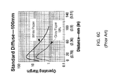
- a margin value corresponds to a specific distance between a target to be sensed and the front of the receiving lens of the sensor, and typical response curves are often provided for a photoelectric sensor, which show what the typical margin will be depending on the sensing distance.
- a sensing distance for a diffuse type sensor is defined as the distance from the front of the receiving lens of a sensor to the specified target.
- Photoelectric sensors are often characterized in terms of their maximum and minimum sensing distances. Often a "blind area" exists in which a target that is too close to the sensor can not be sensed because the light reflected from the target is not received by the photodetector. This occurs in the case of a diffuse sensor because the light source and the photodetector are combined within the same housing such that the emitted light and the light reflected from the target to be detected and received by the sensor each travel along different paths, and the reflected light enters the sensor at an angle with respect to the emitted light. The closer a target is to the sensor, the greater is the angle of the reflected light. At some point, the angle between the paths becomes so great that no light can be received by the photodetector.
- an improved photoelectric sensor can overcome one or more of these disadvantages by using a refraction block to refract reflected light from a target to a photodetector surface.
- such an improved photoelectric sensor can operate by employing an emitting portion for emitting light to a target and a receiving portion for receiving, through a receive lens, reflected light that is at least some of the emitted light that is reflected by a target, and a refraction block having a block first surface and a block second surface, wherein the reflected light received from the receive lens is refracted by at least one of the block surfaces as it passes through the refraction block.
- the sensor also includes a photodetector for receiving the reflected light refracted by the refraction block and provides a detection signal indicative of the reflected light received by the photodetector.
- the present invention relates to a method for sensing a target that includes emitting light towards a target from a light source situated in an emitting portion, and receiving through a receive lens reflected light that is at least some of the emitted light that is reflected by the target.
- the method further includes receiving the reflected light from the receive lens at a refraction block that includes a block first surface and a block second surface, and refracting the reflected light using at least one of the block surfaces.
- the method additionally includes receiving the reflected light from the block second surface at a photodetector surface, and generating a signal indicative of the reflected light received at the photodetector surface.
- FIG. 1A is a front perspective view of an exemplary photoelectric sensor
- FIG. 1B is a rear perspective view of the photoelectric sensor of FIG. 1 A;
- FIG. 1C is a front perspective view of the photoelectric sensor of FIG. 1A when also including a parent circuit board;
- FIG. 1D is an exploded front perspective view of the photoelectric sensor of FIG. 1A depicting various additional components;
- FIG. 1E is a back perspective view of the photoelectric sensor of FIG. 1D ;
- FIG. 2 is a cross-sectional side view of the photoelectric sensor of FIG. 1 A;
- FIG. 3A is a front perspective view of a refraction block shown in FIG. 2 ;
- FIG. 3B is a rear perspective view of the refraction block shown in FIG. 2 ;
- FIG. 4A is a cross-sectional side view of the photoelectric sensor of FIG. 1A , and depicting a light response to a short-range target;
- FIG. 4B is a cross-sectional side view of the photoelectric sensor of FIG. 1A modified so as not to include a refraction block and depicting a light response to a short-range target;
- FIG. 4C is a cross-sectional side view of the photoelectric sensor of FIG. 2 depicting a light response to a long-range target;
- FIG. 4D is a cross-sectional side view of the sensor of FIG. 4C modified so as not to include a refraction block and depicting a light response to a long-range target;
- FIG. 5A is an exploded front perspective view of the photoelectric sensor of FIG. 1A ;
- FIG. 5B is an exploded back perspective view of the photoelectric sensor of FIG. 1A ;
- FIG. 6A is a graph of the margin value of the sensor with respect to the sensing distance of a target
- FIG. 6B is a table of values taken from the graph of FIG. 6A ;
- FIG. 6C is a graph of a margin value of a prior art sensor with respect to the sensing distance of a target.
- FIGS. 1A and 1B respectively show front and rear perspective views of the exemplary photoelectric sensor 2.
- FIG. 2 shows a cross-sectional view of the sensor 2 of FIG. 1A operating in relation to an exemplary target 20, which can be any object or structure, the presence or absence of which is of interest.
- exemplary target 20 can be any object or structure, the presence or absence of which is of interest.
- a portion of the space between the sensor 2 and the target 20 is cutaway, and only portions of the light communicated within the sensor 2 and between the sensor2 and the target 20 are shown.
- the photoelectric sensor 2 is configured to emit light toward a predetermined location.
- a target 20 is present at the predetermined location, emitted light directed toward the target is reflected, and reflected light that is at least a portion of the emitted light is received by the sensor 2.
- the sensor 2 includes a refraction block 25 to refract the received reflected light to be measured by a photodetector 27, allowing the sensor 2 to sense both near and far targets with a high margin.
- the senor 2 includes a housing 4 having a front end 6 and a back end 8.
- the housing 4 can be formed as a molded plastic composite, as a single piece or as multiple pieces.
- FIG. 1C depicts the sensor 2 of FIG. 1A which further includes a parent circuit board 9 situated at the back end 8 of the housing 4 for supporting components forming a circuit with the photodetector 27, which circuit generates a signal indicative of the presence of the target 20.
- the senor 2 also includes other components such as, a casing 17, an end plug 19, a connector 21, and a remote adjuster 23. These components are not necessary for the description of the operation of the sensor 2, and for the sake of simplicity, are not shown or described further.
- the sensor 2 includes an emitting portion 10 and a receiving portion 12 arranged adjacent to one another.
- the emitting portion 10 includes a light source 14 for emitting light, such as a light emitting diode (LED) or a laser.
- the light source 14 is situated adjacent the back end 8 of the housing 4.
- the emitting portion 10 can also include an emit lens 16 situated adjacent the housing front end 6.
- the emit lens 16 refracts the light emitted from the light source 14 resulting in emitted light 18 being directed towards the target 20.
- the target 20 reflects at least a portion of the emitted light 18 back towards the sensor 2 as reflected light 22, where it is received by the receiving portion 12 of the sensor 2.
- the receiving portion 12 includes a receive lens 24 and a refraction block 25, which direct the reflected light 22 towards a surface 26 of the photodetector 27.
- a housing aperture 29 is formed in the housing and is situated in between the refraction block 25 and the photodetector surface 26.
- the housing aperture 29 provides a controlled entry point for the reflected light 22 that is directed to the photodetector surface 26.
- the housing aperture 29 can vary in size to accommodate particular applications.
- the photodetector 27 additionally is mounted to a daughter printed circuit board 28 and the daughter printed circuit board 28 is mounted to the parent circuit board 9 as shown in FIG. 1C to form a photodetector circuit 31.
- the photodetector circuit 31 is configured to provide a signal indicative of a sensed characteristic of the target 20. For example, the presence of the target 20 can be indicated by high or low current or voltage if more than a predetermined amount of light is received by the photodetector 27.
- the receive lens 24 has a front surface 30 and a rear surface 32.
- the front and rear surfaces 30, 32 refract and focus the reflected light 22 as it enters and passes through the receive lens 24.
- the front surface 30 is planar and therefore, when reflected light 22 contacts the front surface 30 at a non-perpendicular angle, the front surface 30 refracts the reflected light 22.
- the front surface 30 can be non-planar, such as convex.
- the reflected light 22 is directed from the front surface 30 to the rear surface 32.
- the rear surface 32 is convex, thereby focusing the reflected light 22 as it passes through the rear surface 32 towards the photodetector surface 26.
- the refraction block 25 is positioned in the receiving portion 12, between the receive lens 24 and the photodetector surface 26, as shown in FIG. 2 .
- the refraction block 25 includes a block first surface 34 and a block second surface 36 (see also FIGS. 3A and 3B ), wherein each surface 34, 36 can refract the reflected light 22.
- the block first surface 34 is positioned to receive the reflected light 22 emanating from the rear surface 32 of the receive lens 24.
- the block first surface 34 and the front surface 30 are both substantially planar and parallel to the photodetector surface 26.
- the block second surface 36 is situated at an angle ⁇ with respect to the block first surface 34.
- the refraction block 25 can be formed of a refracting material for transmitting and refracting light, such as an optical acrylic material or polycarbonate material.
- reflected light 22 enters the front surface 30 of the receive lens 24 at an angle of incidence ⁇ . Because the emitting portion 10 and receiving portion 12 are not coaxial, and assuming that, as shown, the emitted light 18 incident upon the target 20 is emitted perpendicularly from the emitting portion 10, the reflected light 22 will have an angle ⁇ that is greater than zero. Without the refraction block 25, the receive lens 24 alone determines the sensor's ability to direct the reflected light 22 to the photodetector surface 26.
- the receive lens 24 has only one surface for refraction and one surface for focusing the reflected light 22, the sensor 2 would have a very limited ability to sense reflected light 22 that is received at an angle ⁇ that is large, which occurs when a target 20 is within close proximity to the sensor 2. In this case, the reflected light 22 reflecting off a close target 20 would not be directed to the photodetector surface 26, and therefore would not be detected. Further, if the angle ⁇ is large, such that only a minimal amount of reflected light 22 (or no reflected light) is able to reach the photodetector surface 26, the margin value of the sensor 2 will be undesirably low at that specific target distance. If the sensor's sensitivity is fixed, the margin curve value of a sensor is largely dependent on the intensity of the light received, less light at the photodetector surface translates into a lower margin value.
- FIG. 4A operation of the refraction block 24 in directing the reflected light 22 within the sensor is shown in more detail.
- the reflected light 22 is refracted at the front surface 30 of the receive lens 24 and is received at the rear surface 32.
- the reflected light 22 is then focused by the rear surface 32 and progresses to the block first surface 34.
- the block first surface 34 substantially refracts the light 22 towards the block second surface 36, which is further refracted by the block second surface 36 and directed towards the photodetector surface 26.
- the light 22 received at the receive lens 24 is redirected towards the photodetector surface 26 by the refraction block 25.
- FIG. 4B depicts the sensor 2 without the refraction block 25, again with a target 20 at a distance of 30 mm from the sensor 2.
- the angle ⁇ becomes large, and less of the reflected light 22 reaches photodetector surface 26.
- the presence of the refraction block 25 allows the sensor 2 to detect the target 20 when otherwise it might not be detectable.
- FIG. 4C shows the presence of the refraction block 25 impedes performance of the sensor 2 in detecting a target that is relatively far away.
- FIG. 4C shows the reflected light 22 from the target 20 when it is 130 mm away from the sensor 2 being received by the receive lens 24.
- the angle ⁇ becomes smaller less of the reflected light 22 is directed to the photodetector surface 26 by the receive lens 24 and the refraction block 25.
- the refraction block 25 directs the reflected light 22 to the photodetector surface 26 for a wide range of angle ⁇ values, when the angle ⁇ becomes too small, a point is reached where the light 22 does not pass through the housing aperture 29 and therefore is prevented from reaching the photodetector surface 26.
- the housing aperture 29 can serve as a pre-defined cut-off for a desired target distance.
- FIG. 4D when the refraction block 25 is not included, only a small portion of the reflected light 22 is received at the photodetector surface 26. As the portion of reflected light 22 is small, the margin value is also small. If the portion of light received becomes too small, the photodetector 26 may not receive enough light to detect the target, thereby creating a blind spot. Further, the sensitivity of the sensor 2 cannot be increased to eliminate the blind spot as this would increase the maximum target sensing range, which is undesirable.
- the refraction block 25 can be configured to compensate for various angles of the reflected light 22 entering the receive lens 24. Further, the refraction block 25 can be positioned at various points along the length of the receive portion 12 (e.g., at different locations between the receive lens 24 and the photodetector surface 26) to further accommodate a specific target distance. Additionally, the angle ⁇ (as seen in FIG.
- the angle ⁇ is about 30 degrees to about 35 degrees. In another embodiment, the angle ⁇ can be between about 5 degrees to about 85 degrees.
- the refraction block 25 is shown as a discrete piece that is insertable into the housing 4.
- the discrete refraction block 25 can be shaped to accommodate various existing sensor housings and can therefore provide the associated benefits without requiring re-tooling of an existing housing.
- the refraction block 25 can be at least partially integral with housing 4.
- an electromagnetic interference (EMI) shield 40 is provided.
- the EMI shield 40 is provided to at least partially block EMI from disrupting the photodetector 27.
- the shield 40 can be comprised of a metal, such as copper, or it can be another material that is at least partially impervious to EMI.
- the shield 40 is positioned substantially between the photodetector 27 and the housing 4.
- the shield 40 includes a shield aperture 42 that substantially aligns with the housing aperture 29 to allow light 22 to pass through the housing aperture 29 to the photodetector surface 26.
- FIG. 6A depicts a graph of the margin achieved by the sensor 2 when the target distance is between 1 and 134 mm, for a white paper target having a reflectivity of 90%, and for a paper target having 18% reflectivity.
- FIG. 6B depicts a chart of values obtained from the graph in FIG. 6A .
- the excess gain is at least 500.
- the excess gain is at least 25, indicating that the sensor 2 lacks a significant blind-spot.
- the margin value drops off to about zero. This indicates that the light 22 is no longer being received at the photodetector surface 26, thereby a sensing cut-off has been established.
- the refraction block 25 allows for extremely high margin values for the sensor 2. The increased margin values provide the sensor 2 the ability to sense very small targets, for example, a target having a diameter as small as 0.1 mm.
Landscapes
- Engineering & Computer Science (AREA)
- Physics & Mathematics (AREA)
- General Physics & Mathematics (AREA)
- Computer Networks & Wireless Communication (AREA)
- Radar, Positioning & Navigation (AREA)
- Remote Sensing (AREA)
- Electromagnetism (AREA)
- Life Sciences & Earth Sciences (AREA)
- General Life Sciences & Earth Sciences (AREA)
- Geophysics (AREA)
- Geophysics And Detection Of Objects (AREA)
- Optical Radar Systems And Details Thereof (AREA)
Applications Claiming Priority (1)
| Application Number | Priority Date | Filing Date | Title |
|---|---|---|---|
| US12/405,528 US7880888B2 (en) | 2009-03-17 | 2009-03-17 | Photoelectric sensor for sensing a target |
Publications (3)
| Publication Number | Publication Date |
|---|---|
| EP2230537A2 true EP2230537A2 (de) | 2010-09-22 |
| EP2230537A3 EP2230537A3 (de) | 2016-12-21 |
| EP2230537B1 EP2230537B1 (de) | 2021-01-13 |
Family
ID=42335163
Family Applications (1)
| Application Number | Title | Priority Date | Filing Date |
|---|---|---|---|
| EP10156781.6A Not-in-force EP2230537B1 (de) | 2009-03-17 | 2010-03-17 | Fotoelektrischer Sensor zum Abtasten eines Targets |
Country Status (3)
| Country | Link |
|---|---|
| US (1) | US7880888B2 (de) |
| EP (1) | EP2230537B1 (de) |
| CN (1) | CN101840004B (de) |
Cited By (1)
| Publication number | Priority date | Publication date | Assignee | Title |
|---|---|---|---|---|
| CN112236941A (zh) * | 2018-06-19 | 2021-01-15 | 弗罗纽斯国际有限公司 | 逆变器壳体 |
Families Citing this family (14)
| Publication number | Priority date | Publication date | Assignee | Title |
|---|---|---|---|---|
| US8542348B2 (en) * | 2010-11-03 | 2013-09-24 | Rockwell Automation Technologies, Inc. | Color sensor insensitive to distance variations |
| EP2508920B1 (de) * | 2011-04-08 | 2016-12-14 | Optosys SA | Verfahren und Vorrichtung zur Überwachung sich bewegender Objekte |
| TWI567953B (zh) * | 2011-12-20 | 2017-01-21 | 新加坡恒立私人有限公司 | 光電模組及包含該模組之裝置 |
| CN102880342B (zh) * | 2012-09-05 | 2018-04-06 | 惠州Tcl移动通信有限公司 | 一种距离传感器组件及移动通信设备 |
| CN103090974B (zh) * | 2013-01-28 | 2015-03-18 | 深圳市共进电子股份有限公司 | 设备指示灯颜色的检测系统 |
| CN103744122B (zh) * | 2013-12-17 | 2017-01-25 | 上海兰宝传感科技股份有限公司 | 零盲区漫反射式光电传感器 |
| JP1518122S (de) * | 2014-06-30 | 2015-02-23 | ||
| AU2017253712B8 (en) * | 2016-04-21 | 2019-11-21 | Apple Inc. | Optical system for reference switching |
| DE112019004295T5 (de) * | 2018-08-30 | 2021-06-02 | Ams Sensors Singapore Pte. Ltd. | Optischer kodierer |
| US20200132219A1 (en) * | 2018-10-31 | 2020-04-30 | Norriseal-Wellmark, Inc. | Smart Valve Position Sensor |
| CN110906961A (zh) * | 2019-12-13 | 2020-03-24 | 上海索迪龙自动化有限公司 | 一种多发射源光电传感器 |
| US12429414B2 (en) * | 2020-01-31 | 2025-09-30 | Kidde Fire Protection, Llc | Method for manufacturing a detector |
| CN111207783A (zh) * | 2020-02-27 | 2020-05-29 | 深圳市欧视达自动化设备有限公司 | 一种应用于漫反射光电传感器的无盲区透镜结构 |
| CN114355466A (zh) * | 2021-12-21 | 2022-04-15 | 上海索迪龙自动化有限公司 | 一种视觉盲区小的光电传感器 |
Family Cites Families (15)
| Publication number | Priority date | Publication date | Assignee | Title |
|---|---|---|---|---|
| US3584223A (en) * | 1969-02-24 | 1971-06-08 | Itek Corp | Optical readout of electric fields by detecting reflected and/or refracted radiation which is incident within the range of variation of the critical angle |
| US4283146A (en) * | 1978-11-30 | 1981-08-11 | Lasag S.A. | Optical detector |
| US4872747A (en) * | 1987-04-15 | 1989-10-10 | Cyberoptics Corporation | Use of prisms to obtain anamorphic magnification |
| JP2855744B2 (ja) * | 1989-02-20 | 1999-02-10 | オムロン株式会社 | 反射形光電スイッチ |
| US5218196A (en) * | 1991-09-05 | 1993-06-08 | Frost Controls, Inc. | Light curtain system with system and watchdog microcontrollers |
| US5557395A (en) * | 1992-10-27 | 1996-09-17 | Omron Corporation | Optical device for measuring speed |
| JPH07140381A (ja) * | 1993-11-18 | 1995-06-02 | Sony Corp | コマ収差補正方法 |
| US5446281A (en) * | 1994-03-24 | 1995-08-29 | Eaton Corporation | Optical sensor with movable refraction element to adjust sensor range |
| JP3617549B2 (ja) * | 1995-03-15 | 2005-02-09 | オムロン株式会社 | 反射型光電センサ |
| US6875975B2 (en) * | 1999-12-24 | 2005-04-05 | Bae Systems Information And Electronic Systems Integration Inc | Multi-color, multi-focal plane optical detector |
| TW513558B (en) * | 2000-10-27 | 2002-12-11 | Fuji Electric Co Ltd | Range finder for automatic focusing |
| EP1421402A2 (de) * | 2001-08-31 | 2004-05-26 | Automotive Distance Control Systems GmbH | Abtastvorrichtung |
| DE10220037C5 (de) * | 2002-05-04 | 2011-02-24 | Sick Ag | Vorrichtung zum Detektieren von Objekten |
| JP2005017382A (ja) * | 2003-06-23 | 2005-01-20 | Sharp Corp | 測距センサおよびこれを備えた電子機器 |
| TWI250301B (en) * | 2004-03-17 | 2006-03-01 | Asia Optical Co Inc | The optical system of laser meter |
-
2009
- 2009-03-17 US US12/405,528 patent/US7880888B2/en active Active
-
2010
- 2010-03-17 CN CN201010139283.XA patent/CN101840004B/zh not_active Expired - Fee Related
- 2010-03-17 EP EP10156781.6A patent/EP2230537B1/de not_active Not-in-force
Non-Patent Citations (1)
| Title |
|---|
| None |
Cited By (2)
| Publication number | Priority date | Publication date | Assignee | Title |
|---|---|---|---|---|
| CN112236941A (zh) * | 2018-06-19 | 2021-01-15 | 弗罗纽斯国际有限公司 | 逆变器壳体 |
| CN112236941B (zh) * | 2018-06-19 | 2023-07-14 | 弗罗纽斯国际有限公司 | 逆变器壳体 |
Also Published As
| Publication number | Publication date |
|---|---|
| EP2230537B1 (de) | 2021-01-13 |
| US7880888B2 (en) | 2011-02-01 |
| US20100238448A1 (en) | 2010-09-23 |
| CN101840004B (zh) | 2014-06-25 |
| CN101840004A (zh) | 2010-09-22 |
| EP2230537A3 (de) | 2016-12-21 |
Similar Documents
| Publication | Publication Date | Title |
|---|---|---|
| US7880888B2 (en) | Photoelectric sensor for sensing a target | |
| EP2241907B1 (de) | Fotoelektrischer Sensor | |
| CN105629213B (zh) | 多传感器接近度感测 | |
| US20030094566A1 (en) | Method and apparatus for self-monitoring of proximity sensors | |
| CA2544600C (en) | Proximity detector | |
| US6392247B1 (en) | Sensor and detection system having wide diverging beam optics | |
| JP2018181191A (ja) | 煙感知器用光センサ | |
| US6225621B1 (en) | Laser photoelectric sensor | |
| US11209527B2 (en) | Optical scanning device | |
| WO2004104959A2 (en) | Smoke detector | |
| JP4432084B2 (ja) | レーザ計測方法、レーザ状態検知機器およびレーザ状態検知システム | |
| US20050201096A1 (en) | Object detecting apparatus for vehicle | |
| US7869048B2 (en) | Photoelectonic sensor | |
| JP2018128905A (ja) | 煙感知器用光センサ | |
| JP5266859B2 (ja) | 光電センサ | |
| GB2404731A (en) | Smoke detector with a surface-mount-device (SMD) light source | |
| JP2002279870A (ja) | 回帰反射形光電センサ | |
| JP3297968B2 (ja) | 限定反射型光電センサ | |
| JP2010256183A (ja) | 反射型光電センサ | |
| US20230236109A1 (en) | Dual-Emitter Optic Block and Chamber for Smoke Detector | |
| CN206133048U (zh) | 基于tir透镜的零盲区漫反射式光电接收透镜 | |
| KR20160038968A (ko) | 광케비티를 갖는 가스센서 조립체 | |
| EP4258013B1 (de) | Optischer sensor zur erkennung von objekten | |
| JP4906626B2 (ja) | 光電センサ | |
| JP3350826B2 (ja) | 限定反射型光電センサ |
Legal Events
| Date | Code | Title | Description |
|---|---|---|---|
| PUAI | Public reference made under article 153(3) epc to a published international application that has entered the european phase |
Free format text: ORIGINAL CODE: 0009012 |
|
| AK | Designated contracting states |
Kind code of ref document: A2 Designated state(s): AT BE BG CH CY CZ DE DK EE ES FI FR GB GR HR HU IE IS IT LI LT LU LV MC MK MT NL NO PL PT RO SE SI SK SM TR |
|
| AX | Request for extension of the european patent |
Extension state: AL BA ME RS |
|
| PUAL | Search report despatched |
Free format text: ORIGINAL CODE: 0009013 |
|
| AK | Designated contracting states |
Kind code of ref document: A3 Designated state(s): AT BE BG CH CY CZ DE DK EE ES FI FR GB GR HR HU IE IS IT LI LT LU LV MC MK MT NL NO PL PT RO SE SI SK SM TR |
|
| AX | Request for extension of the european patent |
Extension state: AL BA ME RS |
|
| RIC1 | Information provided on ipc code assigned before grant |
Ipc: G01V 8/12 20060101ALI20161116BHEP Ipc: G01V 8/10 20060101AFI20161116BHEP |
|
| STAA | Information on the status of an ep patent application or granted ep patent |
Free format text: STATUS: REQUEST FOR EXAMINATION WAS MADE |
|
| 17P | Request for examination filed |
Effective date: 20170616 |
|
| RBV | Designated contracting states (corrected) |
Designated state(s): AT BE BG CH CY CZ DE DK EE ES FI FR GB GR HR HU IE IS IT LI LT LU LV MC MK MT NL NO PL PT RO SE SI SK SM TR |
|
| STAA | Information on the status of an ep patent application or granted ep patent |
Free format text: STATUS: EXAMINATION IS IN PROGRESS |
|
| 17Q | First examination report despatched |
Effective date: 20180111 |
|
| GRAP | Despatch of communication of intention to grant a patent |
Free format text: ORIGINAL CODE: EPIDOSNIGR1 |
|
| STAA | Information on the status of an ep patent application or granted ep patent |
Free format text: STATUS: GRANT OF PATENT IS INTENDED |
|
| INTG | Intention to grant announced |
Effective date: 20200828 |
|
| RIN1 | Information on inventor provided before grant (corrected) |
Inventor name: LIAO, JIANYONG Inventor name: WANG, JIAN HUA |
|
| GRAS | Grant fee paid |
Free format text: ORIGINAL CODE: EPIDOSNIGR3 |
|
| GRAA | (expected) grant |
Free format text: ORIGINAL CODE: 0009210 |
|
| STAA | Information on the status of an ep patent application or granted ep patent |
Free format text: STATUS: THE PATENT HAS BEEN GRANTED |
|
| AK | Designated contracting states |
Kind code of ref document: B1 Designated state(s): AT BE BG CH CY CZ DE DK EE ES FI FR GB GR HR HU IE IS IT LI LT LU LV MC MK MT NL NO PL PT RO SE SI SK SM TR |
|
| REG | Reference to a national code |
Ref country code: GB Ref legal event code: FG4D |
|
| REG | Reference to a national code |
Ref country code: CH Ref legal event code: EP |
|
| REG | Reference to a national code |
Ref country code: DE Ref legal event code: R096 Ref document number: 602010066336 Country of ref document: DE |
|
| REG | Reference to a national code |
Ref country code: IE Ref legal event code: FG4D |
|
| REG | Reference to a national code |
Ref country code: AT Ref legal event code: REF Ref document number: 1353817 Country of ref document: AT Kind code of ref document: T Effective date: 20210215 |
|
| REG | Reference to a national code |
Ref country code: AT Ref legal event code: MK05 Ref document number: 1353817 Country of ref document: AT Kind code of ref document: T Effective date: 20210113 |
|
| REG | Reference to a national code |
Ref country code: NL Ref legal event code: MP Effective date: 20210113 |
|
| REG | Reference to a national code |
Ref country code: LT Ref legal event code: MG9D |
|
| PG25 | Lapsed in a contracting state [announced via postgrant information from national office to epo] |
Ref country code: FI Free format text: LAPSE BECAUSE OF FAILURE TO SUBMIT A TRANSLATION OF THE DESCRIPTION OR TO PAY THE FEE WITHIN THE PRESCRIBED TIME-LIMIT Effective date: 20210113 Ref country code: GR Free format text: LAPSE BECAUSE OF FAILURE TO SUBMIT A TRANSLATION OF THE DESCRIPTION OR TO PAY THE FEE WITHIN THE PRESCRIBED TIME-LIMIT Effective date: 20210414 Ref country code: HR Free format text: LAPSE BECAUSE OF FAILURE TO SUBMIT A TRANSLATION OF THE DESCRIPTION OR TO PAY THE FEE WITHIN THE PRESCRIBED TIME-LIMIT Effective date: 20210113 Ref country code: LT Free format text: LAPSE BECAUSE OF FAILURE TO SUBMIT A TRANSLATION OF THE DESCRIPTION OR TO PAY THE FEE WITHIN THE PRESCRIBED TIME-LIMIT Effective date: 20210113 Ref country code: BG Free format text: LAPSE BECAUSE OF FAILURE TO SUBMIT A TRANSLATION OF THE DESCRIPTION OR TO PAY THE FEE WITHIN THE PRESCRIBED TIME-LIMIT Effective date: 20210413 Ref country code: NL Free format text: LAPSE BECAUSE OF FAILURE TO SUBMIT A TRANSLATION OF THE DESCRIPTION OR TO PAY THE FEE WITHIN THE PRESCRIBED TIME-LIMIT Effective date: 20210113 Ref country code: NO Free format text: LAPSE BECAUSE OF FAILURE TO SUBMIT A TRANSLATION OF THE DESCRIPTION OR TO PAY THE FEE WITHIN THE PRESCRIBED TIME-LIMIT Effective date: 20210413 Ref country code: PT Free format text: LAPSE BECAUSE OF FAILURE TO SUBMIT A TRANSLATION OF THE DESCRIPTION OR TO PAY THE FEE WITHIN THE PRESCRIBED TIME-LIMIT Effective date: 20210513 |
|
| PG25 | Lapsed in a contracting state [announced via postgrant information from national office to epo] |
Ref country code: SE Free format text: LAPSE BECAUSE OF FAILURE TO SUBMIT A TRANSLATION OF THE DESCRIPTION OR TO PAY THE FEE WITHIN THE PRESCRIBED TIME-LIMIT Effective date: 20210113 Ref country code: LV Free format text: LAPSE BECAUSE OF FAILURE TO SUBMIT A TRANSLATION OF THE DESCRIPTION OR TO PAY THE FEE WITHIN THE PRESCRIBED TIME-LIMIT Effective date: 20210113 Ref country code: PL Free format text: LAPSE BECAUSE OF FAILURE TO SUBMIT A TRANSLATION OF THE DESCRIPTION OR TO PAY THE FEE WITHIN THE PRESCRIBED TIME-LIMIT Effective date: 20210113 Ref country code: AT Free format text: LAPSE BECAUSE OF FAILURE TO SUBMIT A TRANSLATION OF THE DESCRIPTION OR TO PAY THE FEE WITHIN THE PRESCRIBED TIME-LIMIT Effective date: 20210113 |
|
| PG25 | Lapsed in a contracting state [announced via postgrant information from national office to epo] |
Ref country code: IS Free format text: LAPSE BECAUSE OF FAILURE TO SUBMIT A TRANSLATION OF THE DESCRIPTION OR TO PAY THE FEE WITHIN THE PRESCRIBED TIME-LIMIT Effective date: 20210513 |
|
| REG | Reference to a national code |
Ref country code: DE Ref legal event code: R097 Ref document number: 602010066336 Country of ref document: DE |
|
| PG25 | Lapsed in a contracting state [announced via postgrant information from national office to epo] |
Ref country code: CZ Free format text: LAPSE BECAUSE OF FAILURE TO SUBMIT A TRANSLATION OF THE DESCRIPTION OR TO PAY THE FEE WITHIN THE PRESCRIBED TIME-LIMIT Effective date: 20210113 Ref country code: EE Free format text: LAPSE BECAUSE OF FAILURE TO SUBMIT A TRANSLATION OF THE DESCRIPTION OR TO PAY THE FEE WITHIN THE PRESCRIBED TIME-LIMIT Effective date: 20210113 Ref country code: MC Free format text: LAPSE BECAUSE OF FAILURE TO SUBMIT A TRANSLATION OF THE DESCRIPTION OR TO PAY THE FEE WITHIN THE PRESCRIBED TIME-LIMIT Effective date: 20210113 Ref country code: SM Free format text: LAPSE BECAUSE OF FAILURE TO SUBMIT A TRANSLATION OF THE DESCRIPTION OR TO PAY THE FEE WITHIN THE PRESCRIBED TIME-LIMIT Effective date: 20210113 |
|
| REG | Reference to a national code |
Ref country code: CH Ref legal event code: PL |
|
| PLBE | No opposition filed within time limit |
Free format text: ORIGINAL CODE: 0009261 |
|
| STAA | Information on the status of an ep patent application or granted ep patent |
Free format text: STATUS: NO OPPOSITION FILED WITHIN TIME LIMIT |
|
| PG25 | Lapsed in a contracting state [announced via postgrant information from national office to epo] |
Ref country code: RO Free format text: LAPSE BECAUSE OF FAILURE TO SUBMIT A TRANSLATION OF THE DESCRIPTION OR TO PAY THE FEE WITHIN THE PRESCRIBED TIME-LIMIT Effective date: 20210113 Ref country code: ES Free format text: LAPSE BECAUSE OF FAILURE TO SUBMIT A TRANSLATION OF THE DESCRIPTION OR TO PAY THE FEE WITHIN THE PRESCRIBED TIME-LIMIT Effective date: 20210113 Ref country code: DK Free format text: LAPSE BECAUSE OF FAILURE TO SUBMIT A TRANSLATION OF THE DESCRIPTION OR TO PAY THE FEE WITHIN THE PRESCRIBED TIME-LIMIT Effective date: 20210113 Ref country code: SK Free format text: LAPSE BECAUSE OF FAILURE TO SUBMIT A TRANSLATION OF THE DESCRIPTION OR TO PAY THE FEE WITHIN THE PRESCRIBED TIME-LIMIT Effective date: 20210113 |
|
| REG | Reference to a national code |
Ref country code: BE Ref legal event code: MM Effective date: 20210331 |
|
| 26N | No opposition filed |
Effective date: 20211014 |
|
| PG25 | Lapsed in a contracting state [announced via postgrant information from national office to epo] |
Ref country code: LU Free format text: LAPSE BECAUSE OF NON-PAYMENT OF DUE FEES Effective date: 20210317 Ref country code: LI Free format text: LAPSE BECAUSE OF NON-PAYMENT OF DUE FEES Effective date: 20210331 Ref country code: CH Free format text: LAPSE BECAUSE OF NON-PAYMENT OF DUE FEES Effective date: 20210331 Ref country code: IE Free format text: LAPSE BECAUSE OF NON-PAYMENT OF DUE FEES Effective date: 20210317 |
|
| PG25 | Lapsed in a contracting state [announced via postgrant information from national office to epo] |
Ref country code: SI Free format text: LAPSE BECAUSE OF FAILURE TO SUBMIT A TRANSLATION OF THE DESCRIPTION OR TO PAY THE FEE WITHIN THE PRESCRIBED TIME-LIMIT Effective date: 20210113 |
|
| PG25 | Lapsed in a contracting state [announced via postgrant information from national office to epo] |
Ref country code: IT Free format text: LAPSE BECAUSE OF FAILURE TO SUBMIT A TRANSLATION OF THE DESCRIPTION OR TO PAY THE FEE WITHIN THE PRESCRIBED TIME-LIMIT Effective date: 20210113 |
|
| PG25 | Lapsed in a contracting state [announced via postgrant information from national office to epo] |
Ref country code: IS Free format text: LAPSE BECAUSE OF FAILURE TO SUBMIT A TRANSLATION OF THE DESCRIPTION OR TO PAY THE FEE WITHIN THE PRESCRIBED TIME-LIMIT Effective date: 20210513 |
|
| PG25 | Lapsed in a contracting state [announced via postgrant information from national office to epo] |
Ref country code: BE Free format text: LAPSE BECAUSE OF NON-PAYMENT OF DUE FEES Effective date: 20210331 |
|
| PG25 | Lapsed in a contracting state [announced via postgrant information from national office to epo] |
Ref country code: HU Free format text: LAPSE BECAUSE OF FAILURE TO SUBMIT A TRANSLATION OF THE DESCRIPTION OR TO PAY THE FEE WITHIN THE PRESCRIBED TIME-LIMIT; INVALID AB INITIO Effective date: 20100317 Ref country code: CY Free format text: LAPSE BECAUSE OF FAILURE TO SUBMIT A TRANSLATION OF THE DESCRIPTION OR TO PAY THE FEE WITHIN THE PRESCRIBED TIME-LIMIT Effective date: 20210113 |
|
| P01 | Opt-out of the competence of the unified patent court (upc) registered |
Effective date: 20230404 |
|
| PG25 | Lapsed in a contracting state [announced via postgrant information from national office to epo] |
Ref country code: MK Free format text: LAPSE BECAUSE OF FAILURE TO SUBMIT A TRANSLATION OF THE DESCRIPTION OR TO PAY THE FEE WITHIN THE PRESCRIBED TIME-LIMIT Effective date: 20210113 |
|
| PGFP | Annual fee paid to national office [announced via postgrant information from national office to epo] |
Ref country code: DE Payment date: 20240220 Year of fee payment: 15 Ref country code: GB Payment date: 20240220 Year of fee payment: 15 |
|
| PGFP | Annual fee paid to national office [announced via postgrant information from national office to epo] |
Ref country code: FR Payment date: 20240220 Year of fee payment: 15 |
|
| PG25 | Lapsed in a contracting state [announced via postgrant information from national office to epo] |
Ref country code: MT Free format text: LAPSE BECAUSE OF FAILURE TO SUBMIT A TRANSLATION OF THE DESCRIPTION OR TO PAY THE FEE WITHIN THE PRESCRIBED TIME-LIMIT Effective date: 20210113 |
|
| REG | Reference to a national code |
Ref country code: DE Ref legal event code: R119 Ref document number: 602010066336 Country of ref document: DE |
|
| GBPC | Gb: european patent ceased through non-payment of renewal fee |
Effective date: 20250317 |
|
| PG25 | Lapsed in a contracting state [announced via postgrant information from national office to epo] |
Ref country code: TR Free format text: LAPSE BECAUSE OF FAILURE TO SUBMIT A TRANSLATION OF THE DESCRIPTION OR TO PAY THE FEE WITHIN THE PRESCRIBED TIME-LIMIT Effective date: 20210113 |
|
| PG25 | Lapsed in a contracting state [announced via postgrant information from national office to epo] |
Ref country code: DE Free format text: LAPSE BECAUSE OF NON-PAYMENT OF DUE FEES Effective date: 20251001 |
|
| PG25 | Lapsed in a contracting state [announced via postgrant information from national office to epo] |
Ref country code: GB Free format text: LAPSE BECAUSE OF NON-PAYMENT OF DUE FEES Effective date: 20250317 |
|
| PG25 | Lapsed in a contracting state [announced via postgrant information from national office to epo] |
Ref country code: FR Free format text: LAPSE BECAUSE OF NON-PAYMENT OF DUE FEES Effective date: 20250331 |