EP2230565A2 - Bilderzeugungsgerät und Bilderzeugungsverfahren - Google Patents
Bilderzeugungsgerät und Bilderzeugungsverfahren Download PDFInfo
- Publication number
- EP2230565A2 EP2230565A2 EP10156746A EP10156746A EP2230565A2 EP 2230565 A2 EP2230565 A2 EP 2230565A2 EP 10156746 A EP10156746 A EP 10156746A EP 10156746 A EP10156746 A EP 10156746A EP 2230565 A2 EP2230565 A2 EP 2230565A2
- Authority
- EP
- European Patent Office
- Prior art keywords
- light
- adjustment
- image forming
- adjustment amount
- control unit
- Prior art date
- Legal status (The legal status is an assumption and is not a legal conclusion. Google has not performed a legal analysis and makes no representation as to the accuracy of the status listed.)
- Withdrawn
Links
- 238000000034 method Methods 0.000 title claims description 18
- 230000007423 decrease Effects 0.000 claims abstract description 39
- 238000003705 background correction Methods 0.000 claims abstract description 38
- 238000010586 diagram Methods 0.000 description 20
- 238000012546 transfer Methods 0.000 description 18
- 230000003287 optical effect Effects 0.000 description 17
- 239000004065 semiconductor Substances 0.000 description 12
- 230000008569 process Effects 0.000 description 11
- 238000012545 processing Methods 0.000 description 8
- 238000012937 correction Methods 0.000 description 7
- 238000001514 detection method Methods 0.000 description 6
- 230000015572 biosynthetic process Effects 0.000 description 4
- 238000009499 grossing Methods 0.000 description 3
- 230000004048 modification Effects 0.000 description 3
- 238000012986 modification Methods 0.000 description 3
- 238000003491 array Methods 0.000 description 2
- 238000006243 chemical reaction Methods 0.000 description 2
- 238000004140 cleaning Methods 0.000 description 2
- 238000005516 engineering process Methods 0.000 description 2
- 230000006870 function Effects 0.000 description 2
- 108091008695 photoreceptors Proteins 0.000 description 2
- 239000002985 plastic film Substances 0.000 description 2
- MCSOAHVAIJXNDN-ZTFGCOKTSA-N ram-322 Chemical compound C1C(=O)CC[C@@]2(O)[C@H]3CC4=CC=C(OC)C(O)=C4[C@]21CCN3C MCSOAHVAIJXNDN-ZTFGCOKTSA-N 0.000 description 2
- XAGFODPZIPBFFR-UHFFFAOYSA-N aluminium Chemical compound [Al] XAGFODPZIPBFFR-UHFFFAOYSA-N 0.000 description 1
- 229910052782 aluminium Inorganic materials 0.000 description 1
- 238000013459 approach Methods 0.000 description 1
- 230000002238 attenuated effect Effects 0.000 description 1
- 230000015556 catabolic process Effects 0.000 description 1
- 230000008859 change Effects 0.000 description 1
- 238000010276 construction Methods 0.000 description 1
- 238000006731 degradation reaction Methods 0.000 description 1
- 238000012217 deletion Methods 0.000 description 1
- 230000037430 deletion Effects 0.000 description 1
- 229920001971 elastomer Polymers 0.000 description 1
- 230000004907 flux Effects 0.000 description 1
- 230000005484 gravity Effects 0.000 description 1
- 238000003384 imaging method Methods 0.000 description 1
- 239000000463 material Substances 0.000 description 1
- 229920006255 plastic film Polymers 0.000 description 1
- 230000009467 reduction Effects 0.000 description 1
- 230000004044 response Effects 0.000 description 1
- 229920002379 silicone rubber Polymers 0.000 description 1
- 230000003068 static effect Effects 0.000 description 1
- 230000002123 temporal effect Effects 0.000 description 1
Images





Classifications
-
- B—PERFORMING OPERATIONS; TRANSPORTING
- B41—PRINTING; LINING MACHINES; TYPEWRITERS; STAMPS
- B41J—TYPEWRITERS; SELECTIVE PRINTING MECHANISMS, i.e. MECHANISMS PRINTING OTHERWISE THAN FROM A FORME; CORRECTION OF TYPOGRAPHICAL ERRORS
- B41J29/00—Details of, or accessories for, typewriters or selective printing mechanisms not otherwise provided for
- B41J29/38—Drives, motors, controls or automatic cut-off devices for the entire printing mechanism
- B41J29/393—Devices for controlling or analysing the entire machine ; Controlling or analysing mechanical parameters involving printing of test patterns
-
- G—PHYSICS
- G03—PHOTOGRAPHY; CINEMATOGRAPHY; ANALOGOUS TECHNIQUES USING WAVES OTHER THAN OPTICAL WAVES; ELECTROGRAPHY; HOLOGRAPHY
- G03G—ELECTROGRAPHY; ELECTROPHOTOGRAPHY; MAGNETOGRAPHY
- G03G15/00—Apparatus for electrographic processes using a charge pattern
- G03G15/22—Apparatus for electrographic processes using a charge pattern involving the combination of more than one step according to groups G03G13/02 - G03G13/20
- G03G15/32—Apparatus for electrographic processes using a charge pattern involving the combination of more than one step according to groups G03G13/02 - G03G13/20 in which the charge pattern is formed dotwise, e.g. by a thermal head
- G03G15/326—Apparatus for electrographic processes using a charge pattern involving the combination of more than one step according to groups G03G13/02 - G03G13/20 in which the charge pattern is formed dotwise, e.g. by a thermal head by application of light, e.g. using a LED array
-
- G—PHYSICS
- G03—PHOTOGRAPHY; CINEMATOGRAPHY; ANALOGOUS TECHNIQUES USING WAVES OTHER THAN OPTICAL WAVES; ELECTROGRAPHY; HOLOGRAPHY
- G03G—ELECTROGRAPHY; ELECTROPHOTOGRAPHY; MAGNETOGRAPHY
- G03G15/00—Apparatus for electrographic processes using a charge pattern
- G03G15/04—Apparatus for electrographic processes using a charge pattern for exposing, i.e. imagewise exposure by optically projecting the original image on a photoconductive recording material
- G03G15/043—Apparatus for electrographic processes using a charge pattern for exposing, i.e. imagewise exposure by optically projecting the original image on a photoconductive recording material with means for controlling illumination or exposure
- G03G15/0435—Apparatus for electrographic processes using a charge pattern for exposing, i.e. imagewise exposure by optically projecting the original image on a photoconductive recording material with means for controlling illumination or exposure by introducing an optical element in the optical path, e.g. a filter
-
- G—PHYSICS
- G03—PHOTOGRAPHY; CINEMATOGRAPHY; ANALOGOUS TECHNIQUES USING WAVES OTHER THAN OPTICAL WAVES; ELECTROGRAPHY; HOLOGRAPHY
- G03G—ELECTROGRAPHY; ELECTROPHOTOGRAPHY; MAGNETOGRAPHY
- G03G2215/00—Apparatus for electrophotographic processes
- G03G2215/04—Arrangements for exposing and producing an image
- G03G2215/0402—Exposure devices
- G03G2215/0404—Laser
Definitions
- the present invention relates to an image forming apparatus and an image forming method.
- a quantity of light on an exposed surface is affected by characteristics of a deflecting element, which deflects light beam, and a lens, so even when a light source emits light beam at a constant light quantity, the light beam onto the exposed surface is not constant in light quantity. Consequently, there is a variation in an electrostatic latent image on a recording medium, and a developed image is lacking in uniformity, which shows up as perceived banding on a finally-formed image, whereby an image quality is affected.
- an image quality is improved with use of an optical element, for example, by using a lens having a characteristic capable of preventing a light quantity on the exposed surface from varying or by placing a filter on an optical path.
- a shading correction is performed by performing pulse-width modulation or phase modulation of a drive voltage of a light-source drive element (for example, see Japanese Patent Application Laid-open No. 2002-172817 ).
- correction characteristics represents a continuous correction curve in accordance with optical characteristics of a lens and the like as shown in Fig. 11 , so if the shading correction is performed by the pulse-width modulation of a drive voltage of a light-source drive element, the number of gradations has to be increased, and in a configuration of an apparatus, for example, it brings an excessive increase in Look Up Table (LUT) or an excessive increase in circuit size for high-speed processing and the like.
- LUT Look Up Table
- the correction curve is not smooth and has steps as shown in Fig. 12 , which contributes to an uneven image around the steps, and furthermore, it is necessary to provide a filter element on the outside, and the apparatus configuration increases excessively.
- the present invention is made in consideration of the above, and an object of the present invention is to provide an image forming apparatus and an image forming method capable of obtaining a high-quality image reduced in density fluctuation by performing a smooth shading correction in accordance with optical characteristics without increasing an apparatus configuration excessively.
- an image forming apparatus that performs a shading correction includes a light source that emits a light beam; a light-source drive unit that drives the light source; and a light-quantity-adjustment-amount control unit that performs an adjustment of a light quantity in accordance with a shading correction curve by controlling, for the light-source drive unit, a light-quantity adjustment amount and an increase/decrease cycle of the light-quantity adjustment amount.
- the increase/decrease cycle is a unit of time within a time period during which the light-quantity adjustment amount increases or decreases.
- Fig. 1 is a schematic diagram illustrating a mechanical configuration of an image forming apparatus according to a first embodiment.
- An image forming apparatus 100 is composed of an optical device 102 including optical elements, such as a VCSEL 200 (see Figs. 2A, 2B , and 3 ) and a polygon mirror 102a, an image forming unit 112 including photosensitive drums, charging devices, developing devices, and the like, and a transfer unit 122 including an intermediate transfer belt.
- the optical device 102 includes the VCSEL 200 as a semiconductor laser.
- light beams emitted from the VCSEL 200 (not shown in Fig. 1 ) are first collected by a first cylindrical lens (not shown), and deflected to respective reflection mirrors 102b by the polygon mirror 102a.
- Fig. 2A vertical arrays of the light sources are denoted by a to c, and lateral arrays are denoted by 1 to 4; for example, the top-left light source 1001 in Fig. 2A is denoted by a1. Since the light sources 1001 are obliquely arranged at a polygon mirror angle ⁇ with respect to a sub-scanning direction, it is assumed that the light source a1 and the light source a2 expose different scanning positions to light, and a pixel (one pixel) is constructed by this two light sources, i.e., in Fig. 2A , one pixel is achieved by two light sources.
- Fig. 2B is a configuration diagram of another example of the VCSEL 200.
- the light sources 1001 are arranged at the positions displaced in a sub-scanning direction.
- a center-to-center distance between the two light sources (n dpi in Fig. 2B ) is equivalent to 2400 dpi, and is equivalent to 4800 dpi at a portion near the center thereof, which is an non-uniform arrangement.
- the exposure is performed by means of an interlaced scanning.
- light beams L respectively corresponding to cyan (C), magenta (M), yellow (Y), and black (K) image data are emitted, and reflected by the reflection mirrors 102b, and then again collected by second cylindrical lenses 102c, and after that, photosensitive drums 104a, 106a, 108a, and 110a are exposed to the light beams L, respectively.
- Each of the photosensitive drums 104a, 106a, 108a, and 110a includes a photoconductive layer including at least a charge generation layer and a charge transport layer on a conductive drum made of aluminum or the like.
- the photoconductive layers are provided to correspond to the photosensitive drums 104a, 106a, 108a, and 110a, and applied with surface charges by charger units 104b, 106b, 108b, and 110b each including a corotron, a scorotron, or a charging roller, respectively.
- Static charges applied to the photosensitive drums 104a, 106a, 108a, and 110a by the respective charger units 104b, 106b, 108b, and 110b are exposed to the light beams L, and electrostatic latent images are formed.
- the electrostatic latent images formed on the photosensitive drums 104a, 106a, 108a, and 110a are developed by developing units 104c, 106c, 108c, and 110c each including a developing sleeve, a developer supply roller, a control blade, and the like, respectively, and developer images are formed.
- the developer images formed on the photosensitive drums 104a, 106a, 108a, and 110a are transferred onto an intermediate transfer belt 114, which moves in a direction of an arrow A in accordance with rotation of conveying rollers 114a, 114b, and 114c, in a superimposed manner.
- the superimposed C, M, Y, and K developer images (hereinafter, referred to as a "multicolor developer image") transferred onto the intermediate transfer belt 114 are conveyed to a secondary transfer unit in accordance with the movement of the intermediate transfer belt 114.
- the secondary transfer unit includes a secondary transfer belt 118 and conveying rollers 118a and 118b.
- the secondary transfer belt 118 moves in a direction of an arrow B in accordance with rotation of the conveying rollers 118a and 118b.
- An image receiving medium 124 such as high-quality paper or a plastic sheet, is fed from an image-receiving-media containing unit 128, such as a paper cassette, to the secondary transfer unit by a conveying roller 126.
- the secondary transfer unit applies a secondary bias to the intermediate transfer belt 114, whereby the multicolor developer image on the intermediate transfer belt 114 is transferred onto the image receiving medium 124 attracted and held on the secondary transfer belt 118.
- the image receiving medium 124 is supplied to a fixing unit 120 in accordance with the movement of the secondary transfer belt 118.
- the fixing unit 120 includes a fixing member 130, such as a fixing roller made of silicon rubber or fluorine-contained rubber, and applies heat and pressure to the image receiving medium 124 and the multicolor developer image, and outputs the image receiving medium 124 as a printed material 132 to outside the image forming apparatus 100.
- a cleaning unit 116 including a cleaning blade removes transfer residual developers from the intermediate transfer belt 114 to make ready for a next image forming process.
- Fig. 3 is a schematic perspective view illustrating a case where the optical device 102 including the VCSEL 200 exposes the photosensitive drum 104a to light beams L.
- the light beams L emitted from the VCSEL 200 are collected by a first cylindrical lens 202 used to shape a light beam flux, and goes through a reflection mirror 204 and an imaging lens 206, and then is deflected by the polygon mirror 102a.
- the polygon mirror 102a is driven to spin several thousand times to tens of thousands times by a spindle motor or the like.
- the light beam L After the light beam L reflected by the polygon mirror 102a is reflected by the reflection mirror 102b, the light beam L passes through f ⁇ lens (not shown) and is again shaped by the second cylindrical lens 102c, then hits the photosensitive drum 104a, i.e., the photosensitive drum 104a is exposed to the light beam L.
- a reflection mirror 208 is arranged.
- the reflection mirror 208 reflects the light beam L to a synchronization detection device 210 including a photodiode and the like before the scanning in the sub-scanning direction is started.
- the synchronization detection device 210 When detecting the light beam, the synchronization detection device 210 generates a synchronization signal to start sub-scanning, and synchronizes a process, such as a process of generating a drive control signal to the VCSEL 200.
- the VCSEL 200 is driven by a pulse signal sent from a write control unit 310 to be described later, and as described later, the position of the photosensitive drum 104a corresponding to predetermined image bits of image data is exposed to the light beam L, and an electrostatic latent image is formed on the photosensitive drum 104a.
- Fig. 4 is a schematic functional block diagram of a control unit 300 of the image forming apparatus 100.
- the control unit 300 includes a scanner unit 302, a printer unit 308, and a main control unit 330.
- the scanner unit 302 functions as a means for reading an image, and includes a VPU 304 and an IPU 306.
- the VPU 304 converts an analog signal read by a scanner into a digital signal, and performs a black offset correction, a shading correction, and a pixel location correction.
- the IPU 306 performs image processing mainly for converting the acquired image in the RGB color system into digital image data in the CMYK color system.
- the read image acquired by the scanner unit 302 is output as digital data to the printer unit 308.
- the printer unit 308 includes the write control unit 310, an LD driver 312, and the VCSEL 200.
- the write control unit 310 functions as a control means for performing the drive control of the VCSEL 200.
- the LD driver 312 supplies a current for driving a semiconductor laser element to the semiconductor laser element in response to a drive control signal generated by the write control unit 310.
- the VCSEL 200 mounts thereon two-dimensionally-arranged semiconductor laser elements.
- the write control unit 310 executes high-resolution processing on the image data transmitted from the scanner unit 302 by dividing pixel data in a size corresponding to the spatial size of the semiconductor laser elements of the VCSEL 200.
- the scanner unit 302 and the printer unit 308 are connected to the main control unit 330 via a system bus 316, and image reading and image formation are controlled by a command from the main control unit 330.
- the main control unit 330 includes a central processing unit (CPU) 320 and a RAM 322.
- the RAM 322 provides a processing space used by the CPU 320 for processing. Any CPUs that have been known can be used as the CPU 320; for example, a CISC (Complex Instruction Set Computer), such as the PENTIUM (registered trademark) series and a PENTIUM-compatible CPU, a RISK (Reduced Instruction Set Computer), such as the MIPS, and the like can be used.
- the CPU 320 receives an instruction from a user via an interface 328, and calls a program module for executing a process corresponding to the instruction to execute the process, such as copy, fax, scan, or image storage.
- the main control unit 330 further includes a ROM 324, and the ROM 324 stores therein default setting data of the CPU 320, control data, a program, and the like so as to be used by the CPU 320.
- An image storage 326 is configured as a fixed memory device or removable memory device, such as a hard disk device, an SD card, and a USB memory, and stores therein image data acquired by the image forming apparatus 100 so that the image data can be used for various processes by a user.
- the CPU 320 executes the main scanning direction control and the sub-scanning position control of an image receiving medium, such as high-quality paper or a plastic film.
- the CPU 320 outputs a start signal to the write control unit 310.
- the write control unit 310 receives the start signal, the IPU 306 starts a scanning process. After that, the write control unit 310 receives image data stored in a buffer memory or the like, and processes the received image data, and then outputs the processed image data to the LD driver 312.
- Laser beams onto a photoreceptor are attenuated by passing through lenses and the like, and affected by characteristics of the lenses, so that even if the laser beams are constant in light quantity at the light-source outlets, a light intensity differs among the laser beams depending on the main scanning position. If an image height on the middle of the photoreceptor is set as 0, for example, a light-quantity distribution as shown in Fig. 11 is obtained. It shows that to implement a light-quantity correction of the light-quantity distribution shown in Fig. 11 so as to be identical to a light quantity at the image height of 0 in a whole image height, a light quantity at an image-height end portion is increased, and the light quantity is controlled not to be increased gradually as the image height approaches 0.
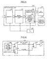
- Fig. 5 is a detailed functional block diagram of the write control unit 310.
- the write control unit 310 receives a synchronization signal, and includes a memory 340 such as a FIFO buffer for storing and memorizing image data sent from the IPU 306, and passes the image data sent from the IPU 306 to an image processing unit 342 via the memory 340.
- the image processing unit 342 reads the image data from the memory 340, and executes processes of a resolution conversion of the image data, an allocation of the channel of the semiconductor laser element, and addition/deletion of image bits (i.e., corrected pixel for enlargement/reduction of the image data) (i.e., a correction process of the image data).
- the position of the photosensitive drum 104a exposed to light beams corresponding to the image data is defined by a main-scanning line address value defining the main scanning direction and a sub-scanning line address value defining the sub-scanning direction.
- An output-data control unit 344 adjusts light quantity of the VCSEL 200, and sends a drive control signal of the VCSEL 200 to the LD driver 312.
- the output-data control unit 344 includes a light-quantity-adjustment-amount control unit 345 for controlling the adjustment of light quantity of the VCSEL 200 by the LD driver 312.
- the light-quantity-adjustment-amount control unit 345 controls a light-quantity adjustment amount for the LD driver 312 to adjust a quantity of light emitted from the VCSEL 200.
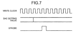
- Fig. 6 is an explanatory diagram of detailed configurations of interfaces of the light-quantity-adjustment-amount control unit 345 and the LD driver 312.
- the light-quantity-adjustment-amount control unit 345 is provided with a DAC-setting-value/strobe deriving unit 355 and flip-flop circuits 351 and 352.
- the LD driver 312 is provided with a flip-flop circuit 353 and a shading correction DAC (D/A converter) 354.
- the DAC-setting-value/strobe deriving unit 355 of the light-quantity-adjustment-amount control unit 345 derives a DAC setting value and a strobe, outputs the DAC setting value to the flip-flop circuit 351, and outputs the strobe to the flip-flop circuit 352.
- a write clock is input to the flip-flop circuits 351 and 352 of the light-quantity-adjustment-amount control unit 345, and the DAC setting value is output as a light-quantity adjustment amount from the flip-flop circuit 351 to the LD driver 312.
- the strobe is output from the flip-flop circuit 352 to the LD driver 312.
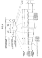
- the number of increases in the light-quantity adjustment amount is set to four.
- the light-quantity-adjustment-amount control unit 345 increases light-quantity adjustment amounts SSn-3' to SSn' in the last time period T1' in the time period T2'; consequently, the corrected light quantity gradually rises by 0.1% to 0.13%.
- the light-quantity-adjustment-amount control unit 345 continues to output the last light-quantity adjustment amount SSn' until it comes to the period of time T3.
- the light-quantity-adjustment-amount control unit 345 outputs the light-quantity adjustment amount S1 from the point of time when it comes to the period of time T3.
- an upper limit to a lower limit of a light-quantity adjustment amount i.e., a limit of resolution in the light-quantity-adjustment-amount control unit 345 is identical to that of the LD driver 312
- a range of the upper limit to the lower limit of the light-quantity adjustment amount in the light-quantity-adjustment-amount control unit 345 is set to be wider than a range of the light quantity of the LD driver 312. Consequently, it is possible to execute a desired shading correction as shown on the top of Fig. 10 .
Landscapes
- Physics & Mathematics (AREA)
- General Physics & Mathematics (AREA)
- Facsimile Scanning Arrangements (AREA)
- Laser Beam Printer (AREA)
- Exposure Or Original Feeding In Electrophotography (AREA)
- Control Or Security For Electrophotography (AREA)
Applications Claiming Priority (2)
| Application Number | Priority Date | Filing Date | Title |
|---|---|---|---|
| JP2009067125 | 2009-03-18 | ||
| JP2010058494A JP5598034B2 (ja) | 2009-03-18 | 2010-03-15 | 画像形成装置および画像形成方法 |
Publications (2)
| Publication Number | Publication Date |
|---|---|
| EP2230565A2 true EP2230565A2 (de) | 2010-09-22 |
| EP2230565A3 EP2230565A3 (de) | 2011-04-27 |
Family
ID=42072913
Family Applications (1)
| Application Number | Title | Priority Date | Filing Date |
|---|---|---|---|
| EP10156746A Withdrawn EP2230565A3 (de) | 2009-03-18 | 2010-03-17 | Bilderzeugungsgerät und Bilderzeugungsverfahren |
Country Status (3)
| Country | Link |
|---|---|
| US (2) | US20100239288A1 (de) |
| EP (1) | EP2230565A3 (de) |
| JP (1) | JP5598034B2 (de) |
Families Citing this family (6)
| Publication number | Priority date | Publication date | Assignee | Title |
|---|---|---|---|---|
| JP5636832B2 (ja) * | 2009-09-15 | 2014-12-10 | 株式会社リコー | 画像形成装置、画像形成方法およびプログラム |
| US8957928B2 (en) | 2010-06-04 | 2015-02-17 | Ricoh Company, Ltd. | Image forming apparatus |
| JP5679110B2 (ja) * | 2011-01-25 | 2015-03-04 | 株式会社リコー | 画像形成装置 |
| JP6277800B2 (ja) | 2014-03-17 | 2018-02-14 | 株式会社リコー | 画像書込装置及び画像形成装置と画像書込方法 |
| JP6642053B2 (ja) | 2016-02-01 | 2020-02-05 | 株式会社リコー | 半導体レーザ駆動装置及び画像形成装置 |
| JP7707814B2 (ja) | 2021-09-30 | 2025-07-15 | 株式会社リコー | 画像形成システム、識別情報印刷方法およびプログラム |
Citations (1)
| Publication number | Priority date | Publication date | Assignee | Title |
|---|---|---|---|---|
| JP2002172817A (ja) | 2000-09-29 | 2002-06-18 | Ricoh Co Ltd | 画像形成装置 |
Family Cites Families (12)
| Publication number | Priority date | Publication date | Assignee | Title |
|---|---|---|---|---|
| JPH0614663B2 (ja) * | 1986-09-19 | 1994-02-23 | 株式会社リコー | 光走査装置 |
| JPH0698104A (ja) * | 1992-09-11 | 1994-04-08 | Ricoh Co Ltd | Ld駆動回路およびシェーディング補正方法 |
| US7161712B2 (en) * | 2001-04-20 | 2007-01-09 | Ricoh Company, Ltd. | Apparatus for forming images with proper gamma correction |
| JP2004338125A (ja) * | 2003-05-13 | 2004-12-02 | Ricoh Co Ltd | 光源制御方法、画像形成方法、画像形成装置及び電子写真装置 |
| JP3938144B2 (ja) * | 2004-02-17 | 2007-06-27 | キヤノン株式会社 | 画像形成装置、その制御方法、及び制御プログラム |
| JP2005262485A (ja) * | 2004-03-16 | 2005-09-29 | Canon Inc | 画像形成装置及びその制御方法 |
| JP4841232B2 (ja) * | 2005-11-09 | 2011-12-21 | 株式会社リコー | レーザ露光装置,画像形成装置および複写装置 |
| JP5043345B2 (ja) * | 2006-02-14 | 2012-10-10 | キヤノン株式会社 | 画像形成装置 |
| JP4912071B2 (ja) * | 2006-08-04 | 2012-04-04 | 株式会社リコー | 光走査装置、光走査方法、画像形成装置、カラー画像形成装置、プログラム、記録媒体 |
| JP4861253B2 (ja) * | 2007-06-12 | 2012-01-25 | 株式会社リコー | 画像処理装置、画像形成装置、プログラムおよび記録媒体 |
| JP2009053466A (ja) * | 2007-08-28 | 2009-03-12 | Kyocera Mita Corp | 画像形成装置 |
| JP5636832B2 (ja) | 2009-09-15 | 2014-12-10 | 株式会社リコー | 画像形成装置、画像形成方法およびプログラム |
-
2010
- 2010-03-15 JP JP2010058494A patent/JP5598034B2/ja not_active Expired - Fee Related
- 2010-03-17 EP EP10156746A patent/EP2230565A3/de not_active Withdrawn
- 2010-03-18 US US12/726,894 patent/US20100239288A1/en not_active Abandoned
-
2012
- 2012-11-13 US US13/675,845 patent/US8605131B2/en not_active Expired - Fee Related
Patent Citations (1)
| Publication number | Priority date | Publication date | Assignee | Title |
|---|---|---|---|---|
| JP2002172817A (ja) | 2000-09-29 | 2002-06-18 | Ricoh Co Ltd | 画像形成装置 |
Also Published As
| Publication number | Publication date |
|---|---|
| EP2230565A3 (de) | 2011-04-27 |
| US8605131B2 (en) | 2013-12-10 |
| JP5598034B2 (ja) | 2014-10-01 |
| JP2010241125A (ja) | 2010-10-28 |
| US20100239288A1 (en) | 2010-09-23 |
| US20130127975A1 (en) | 2013-05-23 |
Similar Documents
| Publication | Publication Date | Title |
|---|---|---|
| US8957928B2 (en) | Image forming apparatus | |
| JP5564806B2 (ja) | 画像形成装置、画像形成方法、画像形成プログラム及び記録媒体 | |
| US9703244B2 (en) | Image forming apparatus to correct a driving signal for driving a light source | |
| US8605131B2 (en) | Image forming apparatus and image forming method | |
| US10133971B2 (en) | Image forming apparatus and method for driving light source | |
| US20110032323A1 (en) | Image forming apparatus, light-intensity correction method, and computer program product | |
| JP5636832B2 (ja) | 画像形成装置、画像形成方法およびプログラム | |
| US20130044176A1 (en) | Optical writing device, image forming apparatus, and method for controlling optical writing device | |
| JP2014015047A (ja) | 画像形成装置、画像形成方法、画像形成プログラム及び記録媒体 | |
| JP4045822B2 (ja) | 画像形成装置 | |
| JP5446635B2 (ja) | 画像形成装置および画像形成方法 | |
| EP1111903A1 (de) | Optisches Schreibgerät und -Verfahren | |
| JP2011189692A (ja) | 光書き込み装置、画像形成装置及び光書き込み装置の制御方法 | |
| JP2019123189A (ja) | 画像形成装置 | |
| JP4403744B2 (ja) | 補正データ生成装置、光プリントヘッドの光量補正方法 | |
| JP5516373B2 (ja) | 画像形成装置、画像形成方法、プログラムおよび記録媒体 | |
| JP5660187B2 (ja) | 画像形成装置、画像形成方法、画像形成プログラム及び記録媒体 | |
| US9417554B2 (en) | Image forming apparatus and image formation method that perform smoothing | |
| JP6740796B2 (ja) | 情報処理装置、画素設定方法、及び、プログラム | |
| JP5614194B2 (ja) | 画像形成装置、画像形成方法、プログラムおよび記録媒体 | |
| JP2006076179A (ja) | プリントヘッド、画像形成装置 | |
| JP2007108576A (ja) | 画像形成装置およびその露光制御方法 | |
| JP2004289303A (ja) | デジタル複写機 | |
| JP2013011765A (ja) | 画像形成装置および画像形成方法 |
Legal Events
| Date | Code | Title | Description |
|---|---|---|---|
| PUAI | Public reference made under article 153(3) epc to a published international application that has entered the european phase |
Free format text: ORIGINAL CODE: 0009012 |
|
| AK | Designated contracting states |
Kind code of ref document: A2 Designated state(s): AT BE BG CH CY CZ DE DK EE ES FI FR GB GR HR HU IE IS IT LI LT LU LV MC MK MT NL NO PL PT RO SE SI SK SM TR |
|
| AX | Request for extension of the european patent |
Extension state: AL BA ME RS |
|
| PUAL | Search report despatched |
Free format text: ORIGINAL CODE: 0009013 |
|
| AK | Designated contracting states |
Kind code of ref document: A3 Designated state(s): AT BE BG CH CY CZ DE DK EE ES FI FR GB GR HR HU IE IS IT LI LT LU LV MC MK MT NL NO PL PT RO SE SI SK SM TR |
|
| AX | Request for extension of the european patent |
Extension state: AL BA ME RS |
|
| 17P | Request for examination filed |
Effective date: 20110829 |
|
| 17Q | First examination report despatched |
Effective date: 20131220 |
|
| STAA | Information on the status of an ep patent application or granted ep patent |
Free format text: STATUS: EXAMINATION IS IN PROGRESS |
|
| STAA | Information on the status of an ep patent application or granted ep patent |
Free format text: STATUS: THE APPLICATION IS DEEMED TO BE WITHDRAWN |
|
| 18D | Application deemed to be withdrawn |
Effective date: 20191011 |