EP2230700A2 - Structure de conditionnement de diode électroluminescente et son procédé de fabrication correspondant - Google Patents
Structure de conditionnement de diode électroluminescente et son procédé de fabrication correspondant Download PDFInfo
- Publication number
- EP2230700A2 EP2230700A2 EP10156859A EP10156859A EP2230700A2 EP 2230700 A2 EP2230700 A2 EP 2230700A2 EP 10156859 A EP10156859 A EP 10156859A EP 10156859 A EP10156859 A EP 10156859A EP 2230700 A2 EP2230700 A2 EP 2230700A2
- Authority
- EP
- European Patent Office
- Prior art keywords
- package structure
- fluorescent layer
- led chip
- led
- light emitting
- Prior art date
- Legal status (The legal status is an assumption and is not a legal conclusion. Google has not performed a legal analysis and makes no representation as to the accuracy of the status listed.)
- Withdrawn
Links
Images


Classifications
-
- H—ELECTRICITY
- H10—SEMICONDUCTOR DEVICES; ELECTRIC SOLID-STATE DEVICES NOT OTHERWISE PROVIDED FOR
- H10H—INORGANIC LIGHT-EMITTING SEMICONDUCTOR DEVICES HAVING POTENTIAL BARRIERS
- H10H20/00—Individual inorganic light-emitting semiconductor devices having potential barriers, e.g. light-emitting diodes [LED]
- H10H20/80—Constructional details
- H10H20/85—Packages
- H10H20/851—Wavelength conversion means
- H10H20/8511—Wavelength conversion means characterised by their material, e.g. binder
- H10H20/8512—Wavelength conversion materials
- H10H20/8513—Wavelength conversion materials having two or more wavelength conversion materials
-
- H—ELECTRICITY
- H10—SEMICONDUCTOR DEVICES; ELECTRIC SOLID-STATE DEVICES NOT OTHERWISE PROVIDED FOR
- H10H—INORGANIC LIGHT-EMITTING SEMICONDUCTOR DEVICES HAVING POTENTIAL BARRIERS
- H10H20/00—Individual inorganic light-emitting semiconductor devices having potential barriers, e.g. light-emitting diodes [LED]
- H10H20/01—Manufacture or treatment
- H10H20/036—Manufacture or treatment of packages
- H10H20/0361—Manufacture or treatment of packages of wavelength conversion means
-
- H—ELECTRICITY
- H10—SEMICONDUCTOR DEVICES; ELECTRIC SOLID-STATE DEVICES NOT OTHERWISE PROVIDED FOR
- H10H—INORGANIC LIGHT-EMITTING SEMICONDUCTOR DEVICES HAVING POTENTIAL BARRIERS
- H10H20/00—Individual inorganic light-emitting semiconductor devices having potential barriers, e.g. light-emitting diodes [LED]
- H10H20/80—Constructional details
- H10H20/85—Packages
- H10H20/852—Encapsulations
-
- H—ELECTRICITY
- H10—SEMICONDUCTOR DEVICES; ELECTRIC SOLID-STATE DEVICES NOT OTHERWISE PROVIDED FOR
- H10W—GENERIC PACKAGES, INTERCONNECTIONS, CONNECTORS OR OTHER CONSTRUCTIONAL DETAILS OF DEVICES COVERED BY CLASS H10
- H10W72/00—Interconnections or connectors in packages
- H10W72/01—Manufacture or treatment
- H10W72/015—Manufacture or treatment of bond wires
- H10W72/01515—Forming coatings
-
- H—ELECTRICITY
- H10—SEMICONDUCTOR DEVICES; ELECTRIC SOLID-STATE DEVICES NOT OTHERWISE PROVIDED FOR
- H10W—GENERIC PACKAGES, INTERCONNECTIONS, CONNECTORS OR OTHER CONSTRUCTIONAL DETAILS OF DEVICES COVERED BY CLASS H10
- H10W72/00—Interconnections or connectors in packages
- H10W72/071—Connecting or disconnecting
- H10W72/075—Connecting or disconnecting of bond wires
-
- H—ELECTRICITY
- H10—SEMICONDUCTOR DEVICES; ELECTRIC SOLID-STATE DEVICES NOT OTHERWISE PROVIDED FOR
- H10W—GENERIC PACKAGES, INTERCONNECTIONS, CONNECTORS OR OTHER CONSTRUCTIONAL DETAILS OF DEVICES COVERED BY CLASS H10
- H10W74/00—Encapsulations, e.g. protective coatings
Definitions
- the present invention relates to a semiconductor package structure and a manufacturing method thereof, and more generally to a light emitting diode (LED) package structure and a manufacturing method thereof.
- LED light emitting diode
- a light emitting diode Since a light emitting diode (LED) has such advantages as long service life, small volume, high shock resistance, low heat output and low power consumption, it has been widely applied in indicators or light sources for household appliances and various equipment. In recent years, the LED has been developed towards multicolor and high brightness; therefore, its application scope has been expanded to large outdoor display boards, traffic signal lights and the like. In the future, the LED chip may even become the main illumination light source with both power-saving and environment-protecting functions.
- LED light emitting diode
- a conventional LED package structure is fabricated by a mass production, in which a dispensing process is performed to fill a molding compound into a cave of the chip, and a baking process is then performed to cure the molding compound to complete the LED package structure.
- the molding compound has a fluorescent material therein, and during the step of waiting for the baking process, the fluorescent material is deposited due to the slow filling of the molding compound into the cave of the chip or different timing of filling the molding compound. Accordingly, the distribution of the fluorescent material is not uniform. That is, most portion of the fluorescent material is deposited on the bottom of the cave or the surface of the chip, and only a small portion of the same is distributed in the molding compound sporadically, so as to affect the uniformity of the light emitted from the LED package structure.
- the carriers of the conventional LED package structures have various shapes.
- the equipment has to be adjusted for different carriers. Therefore, the production efficiency is reduced and the fabrication cost is enhanced.
- the present invention provides a LED package structure and a method of fabricating the same, so as to enhance the light-emitting uniformity of the LED package structure.
- the present invention provides a method of fabricating a LED package structure.
- First, at least one LED chip is provided.
- the LED chip is disposed on a carrier and has a light emitting surface and a plurality of side surfaces connected to the light emitting surface.
- a first mask is provided.
- the first mask has at least one first opening, and the first opening at least exposes the LED chip.
- a spray coating apparatus is provided.
- the spray coating apparatus is disposed above the first mask to perform a first spray coating process.
- the spray coating apparatus moves back and forth to spray a first phosphor solution over the LED chip so that the light-emitting surface and the side surfaces of the LED chip can be conformally covered by the sprayed first phosphor solution.
- a curing process is then performed, so as to cure the first phosphor solution on the light emitting surface and the side surfaces of the LED chip to form a first fluorescent layer. Further, a molding compound is formed to encapsulate the first fluorescent layer and a portion of the carrier.
- the first phosphor solution includes a solvent, a gel and a fluorescent powder.
- the method further includes performing a first heating process on the LED chip and the carrier to evaporate the solvent in the first phosphor solution on the LED chip.
- the method further includes removing the first mask. Thereafter, a second mask is provided above the LED chip.
- the second mask has at least one second opening smaller than the first opening, and the second opening correspondingly exposes a portion of the first phosphor solution on the light emitting surface of the LED chip.
- a second spray coating process is performed. The spray coating apparatus moves back and forth to spray a second phosphor solution on the portion of the first phosphor solution exposed by the second opening.
- the second phosphor solution includes a solvent, a gel and fluorescent powder.
- the solvent includes xylene, n-heptane or acetone.
- the gel includes silicone or silica gel or epoxy resin.
- the solvent, the gel and the fluorescent powder respectively account for about 50%, 20% and 30% in the first phosphor solution.
- the method further includes performing a second heating process to evaporate the solvent in the second phosphor solution on the LED chip.
- the spray coating apparatus includes a spray nozzle, and the spray nozzle sprays the first phosphor solution and the second phosphor solution on the LED chip respectively by atomization.
- the method further includes curing the second phosphor solution on the LED chip to form a second fluorescent layer.
- the method further comprises forming at least one wire, and the LED chip is electrically connected to the carrier through the wire.
- the carrier includes a circuit board or a lead frame.
- the present invention further provides a LED package structure including a LED chip, a first fluorescent layer, a second fluorescent layer and a molding compound.
- the LED chip is disposed on a carrier and has a light emitting surface and a plurality of side surfaces connected to the light emitting surface.
- the first fluorescent layer conformally covers the light emitting surface and the side surfaces of the LED chip.
- the second fluorescent layer is disposed on a portion of the first fluorescent layer on the light emitting layer of the LED chip.
- the lens is disposed on the first fluorescent layer, the second fluorescent layer and a portion of the carrier.
- the first fluorescent layer includes a gel and a fluorescent powder.
- the gel includes silicone or silica gel or epoxy resin.
- the second fluorescent layer includes a gel and a fluorescent powder.
- the second fluorescent layer has substantially the same thickness on the first fluorescent layer.
- the thickness of the second fluorescent layer is smaller than, equal than or greater than that of the first fluorescent layer.
- the thickness of the first fluorescent layer is between about 10 ⁇ m and 30 ⁇ m
- the thickness of the second fluorescent layer is between about 10 ⁇ m and 20 ⁇ m.
- the LED package structure further includes at least one wire, and the LED chip is electrically connected to the carrier through the wire.
- the carrier includes a circuit board or a lead frame.
- the phosphor solution is sprayed on the light emitting surface and the side surfaces of the LED chip, and the fluorescent layer has substantially the same thickness on the light emitting surface and the side surfaces of the LED chip. That is, the fluorescent layer is disposed on the emitting surface and the side surfaces of the LED chip with a uniform thickness, and the thickness of the fluorescent layer on the light emitting layer is substantially the same as that on each side surface. Therefore, when the light emitted from the LED chip is transmitted to the external environment through the molding compound, the LED package structure has better light emitting uniformity.
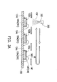
- FIG 1 schematically illustrates a cross-sectional view of a LED package structure according to an embodiment of the present invention.
- FIG. 2 illustrates a flow chart of a method of fabricating a LED package structure according to an embodiment of the present invention.
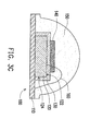
- FIGs. 3A to 3C schematically illustrate cross-sectional views of a method of fabricating a LED package structure according to an embodiment of the present invention.
- FIG. 1 schematically illustrates a cross-sectional view of a LED package structure according to an embodiment of the present invention.
- the LED package structure 100 includes a carrier 110, a LED chip 120, a first fluorescent layer 130, a second fluorescent layer 140 and a lens, for example a molding compound 150.
- the LED chip 120 is disposed on the carrier 110.
- the LED chip 120 has a light emitting surface 122 and a plurality of side surfaces 124 connected to the light emitting surface 122.
- the LED chip 120 is electrically connected to the carrier 110 through at least one wire 160 ( FIG. 1 only schematically illustrates one wire for illustration purposes).
- the carrier 110 is a circuit board or a lead frame, for example.
- the LED chip 120 includes a blue LED chip, a red LED chip, a green LED chip or a purple LED chip, for example.
- the first fluorescent layer 130 is disposed on the LED chip 120 and conformally covers the light emitting surface 122 and the side surfaces 124 of the LED chip 120.
- the first fluorescent layer 130 has substantially the same thickness on the light emitting surface 122 and the side surfaces 124. That is, the first fluorescent layer 130 is disposed on the light emitting surface 122 and the side surfaces 124 of the LED chip 120 with a uniform thickness, and the thickness of the first fluorescent layer 130 on the light emitting surface 122 is substantially the same as that on each side surface 124.
- the first fluorescent layer 130 includes a gel and a fluorescent powder.
- the second fluorescent layer 140 is disposed on a portion of the first fluorescent layer 130 on the light emitting surface 122 of the LED chip 120.
- the second fluorescent layer 140 has substantially the same thickness on the first fluorescent layer 130. That is, the second fluorescent layer 140 is disposed on the portion of the first fluorescent layer 130 on the light emitting surface 122 of the LED chip 120 with a uniform thickness. Further, in this embodiment, the thickness of the second fluorescent layer 140 can be greater than, smaller than or equal to that of the first fluorescent layer 130. Preferably, the thickness of the first fluorescent layer 130 is between about 10 ⁇ m and 30 ⁇ m, and thickness of the second fluorescent layer 140 is between 10 ⁇ m and 20 ⁇ m.
- the second fluorescent layer 140 includes a gel and a fluorescent powder.
- the fluorescent powder of the first fluorescent layer 130 is substantially the same as that of the second fluorescent layer 140, but the present invention is not limited thereto. It is appreciated by persons skilled in the art that the first fluorescent layer 130 and the second fluorescent layer 140 can have different fluorescent powders upon request.
- the molding compound 150 encapsulates the first fluorescent layer 130, the second fluorescent layer 140, the wire 160 and a portion of the carrier 110.
- the molding compound is for protecting the LED chip 120 and the wire 160 from being affected by the temperature, humidity and signals in the external environment.
- the molding compound includes silicone or silica gel or epoxy resin, for example.
- the color light emitted from the light emitting surface 122 or the side surfaces 124 of the LED chip 120 is transmitted to the external environment through the molding compound 150.
- a portion of the color light emitted from the LED chip 120 irradiates the first fluorescent layer 130 and the second fluorescent layer 140 from the light emitting surface 122, and another portion of the same irradiates the first fluorescent layer 130 from the side surfaces 124.
- the color light emitted from the LED chip 120 respectively excites the fluorescent powders in the first fluorescent layer 130 and the second fluorescent layer 140 to emit another color light, which is mixed with the color light emitted from the LED chip 120 itself to form white light as seen by human eyes.
- the first fluorescent layer 130 is disposed on the light emitting surface 122 and the side surfaces 124 of the LED chip 120 with a uniform thickness
- the second fluorescent layer 140 is disposed on a portion of the first fluorescent layer 130 on the light emitting surface 122 of the LED chip 120 with a uniform thickness. Therefore, the mixed color light of the color light emitted from the first fluorescent layer 130 and the second fluorescent layer 140 and the color light emitted from the LED chip 120 itself has a better uniformity. That is, when the mixed color light is transmitted to the external environment through the light-transmissive molding compound 150, the uniformity of the light emitted from the LED package structure 100 over all angles is better. In other words, the LED package structure 100 of the present invention has better light emitting uniformity.
- the present invention also provides a method of fabricating a LED package structure.
- the manufacturing method is depicted with accompanying diagrams of FIGs. 2 and 3A-3C , wherein the LED package structure 100 in FIG. 1 is taken as an example.
- FIG. 2 illustrates a flow chart of a method of fabricating a LED package structure according to an embodiment of the present invention.
- FIGs. 3A to 3C schematically illustrate cross-sectional views of a method of fabricating a LED package structure according to an embodiment of the present invention.
- a carrier 110 and a LED chip array 201 are provided in the step S301.
- the LED chip array 201 includes a first LED chip 120a, a second LED chip 120b and a third LED chip 120c.
- Three LED chips in FIG. 3A are provided for illustration purposes, and are not construed as limiting the present invention.
- the LED chips 120a, 120b and 120c are disposed on a carrier 110.
- Each of the LED chips 120a,120b and 120c respectively has a light emitting surface 122a, 122b and 122c and a plurality of side surfaces 124a, 124b and 124c connected to the emitting surface 122a,122b and 122c.
- Each of the LED chips 120a, 120b and 120c is electronically connected to the carrier 110 through at least one wire 160 ( FIG 3A only schematically illustrates one wire for illustration purposes).
- the carrier 110 includes a circuit board or a lead frame (not shown), for example.
- Each LED chip 120a, 120b and 120c of the LED chip array 201 includes a blue LED chip, a red LED chip, a green LED chip or a purple LED chip, for example.
- a first mask M1 is provided above the LED chip array 201.
- the first mask M1 has at least one first opening 01 ( FIG. 3A only schematically illustrates three first openings for illustration purposes), and these first openings O1 respectively exposes the corresponding light emitting surfaces 122a, 122b and 122c of the LED chips 120a, 120b and 120c and a portion of the carrier 110.
- a spray coating apparatus 200 is provided above the first mask M1 to perform a first spray coating process.
- the spray coating apparatus 200 moves back and forth (the arrow direction in FIG 3A ) to spray a first phosphor solution 130' over the LED chips 120a, 120b and 120c so that the light-emitting surface 122a, 122b and 122c and the side surfaces 124a, 124b and 124c of the LED chips 120a, 120b and 120c can be conformally covered by the sprayed first phosphor solution 130'.
- the first phosphor solution 130' is spray-coated, back and forth along the same path, on the light emitting surfaces 122a, 122b and 122c and the side surfaces 124a, 124b and 124c of the LED chip 120a, 120b and 120c. Therefore, the distribution of the fluorescent powder is substantially the same on the light emitting surface 122a and the side surfaces 124a of the LED chip 120a as well as on the light emitting surface 122c and the side surfaces 124c of the LED chip 120c. Accordingly, the light emitting uniformity of each of the LED chip 120a, 120b and 120c is enhanced.
- the spray coating apparatus 200 includes a two-fluid spray nozzle 202.
- the two-fluid spray nozzle 202 utilizes the theory that compressed air flows in a high speed to atomize the fluid.
- the spray coating apparatus 200 spray-coats the first phosphor solution 130' on the light emitting surfaces 122a, 122b and 122c and the side surfaces 124a, 124b and 124c of the LED chip 120a, 120b and 120c through atomization of the two-fluid spray nozzle 202.
- the first phosphor solution 130' includes a solvent, a gel and a fluorescent powder, for example.
- the solvent includes xylene, n-heptane or acetone, for example.
- the solvent, the gel and the fluorescent powder respectively accounts for about 50%, 20% and 30% in the phosphor solution 130'.
- first phosphor solution 130' is sprayed on the light emitting surfaces 122a, 122b and 122c and the side surfaces 124a, 124b and 124c of the LED chip 120a, 120b and 120c, a first heating process is performed to evaporate the solvent in the first phosphor solution 130'.
- the first phosphor solution 130' of the present invention has the solvent, and the solvent helps to reduce the viscosity of the first phosphor solution 130', so that when the two-fluid spray nozzle 202 is adopted to spray-coat the first phosphor solution 130', the first phosphor solution 130' can distribute uniformly on the light emitting surfaces 122a, 122b and 122c and the side surfaces 124a, 124b and 124c of the LED chip 120a, 120b and 120c. Meanwhile, the first heating process is performed to solidify the first phosphor solution 130'. Therefore, a non-uniform distribution of the fluorescent powder in the first phosphor solution 130' is not observed.
- the first mask M1 is then removed.
- a second mask M2 is provided above the LED chip 120a, 120b and 120c.
- the second mask M2 is disposed between each of the LED chips 120a, 120b and 120c and the spray coating apparatus 200.
- the second mask M2 has at least one second opening 02 ( FIG. 3B only schematically illustrate three second openings for illustration purposes), and these second openings 02 exposes a portion of the first phosphor solution 130' on the corresponding light emitting surfaces 122a, 122b and 122c of the LED chip 120a, 120b and 120c.
- a second spray-coating process is performed.
- the spray coating apparatus 200 moves back and forth (the arrow direction in FIG. 3B ) to spray a second phosphor solution 140' on the portion of the first phosphor solution 130' on the light emitting surfaces 122a, 122b and 122c of the LED chip 120a, 120b and 120c exposed by the second openings 02.
- the second phosphor solution 140' is spray-coated on the portion of the first phosphor solution 130' on the light emitting surfaces 122a, 122b and 122c of the LED chip 120a, 120b and 120c through atomization of the two-fluid spray nozzle 202.
- the second phosphor solution 140' includes a solvent, a gel and a fluorescent powder, for example.
- the solvent includes xylene, n-heptane or acetone, for example.
- the solvent, the gel and the fluorescent powder respectively accounts for about 50%, 20% and 30% in the second phosphor solution 140'.
- the second phosphor solution 140' of the present invention has the solvent, and the solvent helps to reduce the viscosity of the second phosphor solution 140', so that when the two-fluid spray nozzle 202 is adopted to spray the second phosphor solution 140', the second phosphor solution 140' can distribute uniformly on the first phosphor solution 130' on the light emitting surfaces 122a, 122b and 122c of the LED chip 120a, 120b and 120c. Meanwhile, the second heating process is performed to solidify the second phosphor solution 140'. Therefore, a non-uniform distribution of the fluorescent powder in the second phosphor solution 140' is not observed.
- the first phosphor solution 130' is substantially the same as the second phosphor solution 140', but the present invention is not limited thereto. It is for sure that the first phosphor solution 130' can be different from the second phosphor solution 140' due the different fluorescent powders used in the phosphor solutions, which still belong to a technical means adoptable in the present invention and falls within the protection scope of the present invention.
- the first fluorescent layer 130 has substantially the same thickness on the light emitting surfaces 122a, 122b and 122c and the side surfaces 124a, 124b and 124c of the LED chips 120a, 120b and 120c. That is, the first fluorescent layer 130 is disposed on the light emitting surfaces 122a, 122b and 122c and the side surfaces 124a, 124b and 124c of the LED chips 120a, 120b and 120c with a uniform thickness.
- the thickness of the first fluorescent layer 130 on each of the light emitting surfaces 122a, 122b and 122c is the same as that on each of the side surfaces 124a, 124b and 124c.
- the second fluorescent layer 140 has substantially the same thickness on the portion of the first fluorescent layer 130 on the light emitting surfaces 122a, 122b and 122c of the LED chips 120a, 120b and 120c, and the thickness of the second fluorescent layer 140 is smaller than , equal than or greater than that of the first fluorescent layer 130.
- the second mask M2 is then removed.
- a molding compound 150 is formed to encapsulate the first fluorescent layer 130, the second fluorescent layer 140, the wire 160 and a portion of the carrier 110.
- the molding compound 150 is for protecting the LED chips 120a, 120b and 120c and each wire 160 from being affected by the temperature, humidity and signals in the external environment.
- the molding compound includes light-transmissive epoxy resin or silicone, for example.
- a singulation process is preformed to form a plurality of independent LED package structure 100, as shown in FIG. 3C .
- the first phosphor solution 130' is sprayed on the light emitting surfaces 122a, 122b and 122c and the side surfaces 124a, 124b and 124c of the LED chips 120a, 120b and 120c.
- the first fluorescent layer 130 is disposed on the light emitting surfaces 122a, 122b and 122c and the side surfaces 124a, 124b and 124c of the LED chips 120a, 120b and 120c with a uniform thickness.
- the thickness of the first fluorescent layer 130 on each of the light emitting surfaces 122a, 122b and 122c is substantially the same as that on each of the side surfaces 124a, 124b and 124c. Therefore, the light emitting uniformity of each LED package structure 100 is enhanced by the manufacturing method of the present invention.
- the color light emitted from each of the LED chips 120a, 120b and 120c is very directional (i.e. stronger light emitted from the light emitting surface).
- the second mask M2 which has a different dimension from the first mask M1 is used to perform the second spray coating process, so as to form the second fluorescent layer 140 on the first fluorescent layer 130 of the LED chips 120a, 120b and 120c.
- a local multi-phosphor layer structure is formed on each of the LED chips 120a, 120b and 120c, so as to enhance the uniformity of the light emitted from each LED package structure 100.
- the spray coating apparatus 200 sprays the second phosphor solution 140' back and forth along the same path on the first fluorescent layer 130 on the light emitting surfaces 122a, 122b and 122c of the LED chips 120a, 120b and 120c. Accordingly, the second fluorescent layer 140 is disposed on the first fluorescent layer 130 on the light emitting surfaces 122a, 122b and 122c of the LED chips 120a, 120b and 120c with a uniform thickness.
- each LED package structure 100 fabricated by the method of the present invention has better light emitting uniformity.
- the first phosphor solution is sprayed back and forth along the same path on the light emitting surfaces and the side surfaces of the LED chips, and the second phosphor solution is sprayed in the same manner on the first fluorescent layer 130.
- the first fluorescent layer is disposed on the light emitting surfaces and the side surfaces of the LED chips with a uniform thickness
- the second fluorescent layer is disposed on the first fluorescent layer on the light emitting surfaces with a uniform thickness. Therefore, when the color light emitted from the first fluorescent layer and/or the second fluorescent layer is mixed with the color light emitted from each LED chip itself, and the mixed color light is transmitted to the external environment through the molding compound, the uniformity of the light emitted from each LED package structure over all angles is better. In other words, each LED package structure of the present invention has better light emitting uniformity.
Landscapes
- Led Device Packages (AREA)
- Encapsulation Of And Coatings For Semiconductor Or Solid State Devices (AREA)
- Structures Or Materials For Encapsulating Or Coating Semiconductor Devices Or Solid State Devices (AREA)
- Led Devices (AREA)
Applications Claiming Priority (1)
| Application Number | Priority Date | Filing Date | Title |
|---|---|---|---|
| TW098109175A TWI381556B (zh) | 2009-03-20 | 2009-03-20 | 發光二極體封裝結構及其製作方法 |
Publications (2)
| Publication Number | Publication Date |
|---|---|
| EP2230700A2 true EP2230700A2 (fr) | 2010-09-22 |
| EP2230700A3 EP2230700A3 (fr) | 2014-01-01 |
Family
ID=42245597
Family Applications (1)
| Application Number | Title | Priority Date | Filing Date |
|---|---|---|---|
| EP10156859.0A Withdrawn EP2230700A3 (fr) | 2009-03-20 | 2010-03-18 | Structure de conditionnement de diode électroluminescente et son procédé de fabrication correspondant |
Country Status (4)
| Country | Link |
|---|---|
| US (1) | US20100237775A1 (fr) |
| EP (1) | EP2230700A3 (fr) |
| JP (1) | JP5596382B2 (fr) |
| TW (1) | TWI381556B (fr) |
Cited By (2)
| Publication number | Priority date | Publication date | Assignee | Title |
|---|---|---|---|---|
| CN103178194A (zh) * | 2011-12-23 | 2013-06-26 | 山东浪潮华光光电子股份有限公司 | 一种大功率白光led封装结构及其制备方法 |
| WO2014180697A1 (fr) * | 2013-05-06 | 2014-11-13 | Osram Opto Semiconductors Gmbh | Procédé de fabrication d'un composant optoélectronique |
Families Citing this family (48)
| Publication number | Priority date | Publication date | Assignee | Title |
|---|---|---|---|---|
| US10036099B2 (en) | 2008-08-07 | 2018-07-31 | Slt Technologies, Inc. | Process for large-scale ammonothermal manufacturing of gallium nitride boules |
| US9293644B2 (en) | 2009-09-18 | 2016-03-22 | Soraa, Inc. | Power light emitting diode and method with uniform current density operation |
| US8933644B2 (en) | 2009-09-18 | 2015-01-13 | Soraa, Inc. | LED lamps with improved quality of light |
| US10147850B1 (en) | 2010-02-03 | 2018-12-04 | Soraa, Inc. | System and method for providing color light sources in proximity to predetermined wavelength conversion structures |
| US8647900B2 (en) * | 2010-09-20 | 2014-02-11 | Tsmc Solid State Lighting Ltd. | Micro-structure phosphor coating |
| DE102010054280B4 (de) * | 2010-12-13 | 2025-05-22 | OSRAM Opto Semiconductors Gesellschaft mit beschränkter Haftung | Verfahren zum Erzeugen einer Lumineszenzkonversionsstoffschicht, Zusammensetzung hierfür und Bauelement umfassend eine solche Lumineszenzkonversionsstoffschicht |
| US8860056B2 (en) * | 2011-12-01 | 2014-10-14 | Tsmc Solid State Lighting Ltd. | Structure and method for LED with phosphor coating |
| JP5772293B2 (ja) * | 2011-06-28 | 2015-09-02 | 日亜化学工業株式会社 | 発光装置及びその製造方法 |
| JP5817521B2 (ja) * | 2011-12-28 | 2015-11-18 | 日亜化学工業株式会社 | 発光装置の製造方法 |
| JP5712949B2 (ja) * | 2012-02-16 | 2015-05-07 | コニカミノルタ株式会社 | 発光装置の製造方法 |
| WO2013121646A1 (fr) * | 2012-02-16 | 2013-08-22 | コニカミノルタ株式会社 | Procédé de fabrication de dispositif électroluminescent et dispositif d'application de substance fluorescente |
| EP2823515A4 (fr) | 2012-03-06 | 2015-08-19 | Soraa Inc | Diodes électroluminescentes à couches de matériau à faible indice de réfraction destinées à réduire des effets de guidage de lumière |
| US10439112B2 (en) | 2012-05-31 | 2019-10-08 | Cree, Inc. | Light emitter packages, systems, and methods having improved performance |
| US9349929B2 (en) | 2012-05-31 | 2016-05-24 | Cree, Inc. | Light emitter packages, systems, and methods |
| USD709464S1 (en) | 2012-05-31 | 2014-07-22 | Cree, Inc. | Light emitting diode (LED) package |
| USD749051S1 (en) | 2012-05-31 | 2016-02-09 | Cree, Inc. | Light emitting diode (LED) package |
| US10145026B2 (en) | 2012-06-04 | 2018-12-04 | Slt Technologies, Inc. | Process for large-scale ammonothermal manufacturing of semipolar gallium nitride boules |
| CN102751428B (zh) * | 2012-07-20 | 2016-02-17 | 佛山市国星光电股份有限公司 | 一种光转换结构及其制造方法及发光二级管器件 |
| US9978904B2 (en) | 2012-10-16 | 2018-05-22 | Soraa, Inc. | Indium gallium nitride light emitting devices |
| US9761763B2 (en) * | 2012-12-21 | 2017-09-12 | Soraa, Inc. | Dense-luminescent-materials-coated violet LEDs |
| JP5994628B2 (ja) * | 2012-12-26 | 2016-09-21 | 日亜化学工業株式会社 | 発光装置の製造方法およびスプレーコーティング装置 |
| KR101958418B1 (ko) * | 2013-02-22 | 2019-03-14 | 삼성전자 주식회사 | 발광 소자 패키지 |
| JP6233872B2 (ja) * | 2013-03-13 | 2017-11-22 | エムテックスマート株式会社 | Ledの製造方法 |
| DE102013211634A1 (de) * | 2013-06-20 | 2014-12-24 | Osram Opto Semiconductors Gmbh | Verfahren zum Herstellen eines Konversionselements |
| CN104300074B (zh) * | 2013-07-19 | 2017-09-12 | 深圳大学 | 一种荧光粉的涂覆方法及发光二极管装置 |
| JP2015039975A (ja) * | 2013-08-22 | 2015-03-02 | 株式会社World Wing | 自動車用照明装置の製造方法 |
| JP2015041709A (ja) * | 2013-08-22 | 2015-03-02 | 株式会社東芝 | 発光装置 |
| US9410664B2 (en) | 2013-08-29 | 2016-08-09 | Soraa, Inc. | Circadian friendly LED light source |
| JP6713720B2 (ja) * | 2013-08-30 | 2020-06-24 | エルジー イノテック カンパニー リミテッド | 発光素子パッケージ及びそれを含む車両用照明装置 |
| JP6229412B2 (ja) * | 2013-09-30 | 2017-11-15 | 日亜化学工業株式会社 | 発光装置の製造方法 |
| KR101520017B1 (ko) * | 2013-10-10 | 2015-05-14 | 한국생산기술연구원 | 주입유닛을 이용한 발광 다이오드 패키지용 형광층 제조장치, 그리고 이를 이용한 발광 다이오드 패키지용 형광층 제조방법 및 발광 다이오드 패키지 제조방법 |
| US9419189B1 (en) | 2013-11-04 | 2016-08-16 | Soraa, Inc. | Small LED source with high brightness and high efficiency |
| JP6237316B2 (ja) * | 2014-02-18 | 2017-11-29 | 日亜化学工業株式会社 | 発光装置の製造方法および発光装置 |
| JP6237181B2 (ja) * | 2013-12-06 | 2017-11-29 | 日亜化学工業株式会社 | 発光装置の製造方法 |
| DE102014106074A1 (de) * | 2014-04-30 | 2015-11-19 | Osram Opto Semiconductors Gmbh | Leuchtvorrichtung und Verfahren zum Herstellen einer Leuchtvorrichtung |
| US9660151B2 (en) | 2014-05-21 | 2017-05-23 | Nichia Corporation | Method for manufacturing light emitting device |
| JP2016018960A (ja) | 2014-07-10 | 2016-02-01 | エムテックスマート株式会社 | Ledの製造方法及びled |
| JP6428106B2 (ja) * | 2014-09-29 | 2018-11-28 | 日亜化学工業株式会社 | 発光装置及びその製造方法 |
| DE102014116076A1 (de) * | 2014-11-04 | 2016-05-04 | Osram Opto Semiconductors Gmbh | Verfahren zum Aufbringen eines Materials auf einer Oberfläche |
| JP6551015B2 (ja) * | 2015-02-27 | 2019-07-31 | 日亜化学工業株式会社 | 発光装置の製造方法 |
| US20160380162A1 (en) * | 2015-06-26 | 2016-12-29 | Everlight Electronics Co., Ltd. | Light Emitting Device And Manufacturing Method Thereof |
| US10193031B2 (en) * | 2016-03-11 | 2019-01-29 | Rohinni, LLC | Method for applying phosphor to light emitting diodes and apparatus thereof |
| CN107680497B (zh) * | 2017-11-03 | 2019-12-03 | 京东方科技集团股份有限公司 | 显示基板的制造方法、显示基板、显示面板和显示装置 |
| JP2019134150A (ja) * | 2018-01-29 | 2019-08-08 | 日亜化学工業株式会社 | 発光装置 |
| JP6760350B2 (ja) * | 2018-10-25 | 2020-09-23 | 日亜化学工業株式会社 | 発光装置 |
| WO2020182313A1 (fr) * | 2019-03-14 | 2020-09-17 | Osram Opto Semiconductors Gmbh | Composant optoélectronique semi-conducteur et procédé de production d'un composant optoélectronique semi-conducteur |
| CN114156377A (zh) * | 2021-11-30 | 2022-03-08 | 深圳市德明新微电子有限公司 | 一种无模具的led封装方法 |
| CN115579433B (zh) * | 2022-10-28 | 2025-07-08 | 深圳市同一方光电技术有限公司 | 提高产品良率的光源喷粉方法 |
Family Cites Families (19)
| Publication number | Priority date | Publication date | Assignee | Title |
|---|---|---|---|---|
| US6580097B1 (en) * | 1998-02-06 | 2003-06-17 | General Electric Company | Light emitting device with phosphor composition |
| JP4165592B2 (ja) * | 2001-04-17 | 2008-10-15 | 日亜化学工業株式会社 | 発光装置 |
| JP4122738B2 (ja) * | 2001-07-26 | 2008-07-23 | 松下電工株式会社 | 発光装置の製造方法 |
| EP1437776B1 (fr) * | 2001-10-12 | 2011-09-21 | Nichia Corporation | Dispositif d'emission de lumiere et procede de fabrication de celui-ci |
| JP4269709B2 (ja) * | 2002-02-19 | 2009-05-27 | 日亜化学工業株式会社 | 発光装置およびその製造方法 |
| JP4450547B2 (ja) * | 2002-08-29 | 2010-04-14 | 日亜化学工業株式会社 | 発光装置の製造方法 |
| JP5138145B2 (ja) * | 2002-11-12 | 2013-02-06 | 日亜化学工業株式会社 | 蛍光体積層構造及びそれを用いる光源 |
| US7915085B2 (en) * | 2003-09-18 | 2011-03-29 | Cree, Inc. | Molded chip fabrication method |
| JP2006135225A (ja) * | 2004-11-09 | 2006-05-25 | Toshiba Corp | 発光装置 |
| KR101203672B1 (ko) * | 2005-07-01 | 2012-11-23 | 라미나 라이팅, 인크. | 백색 발광 다이오드 및 다이오드 어레이를 포함하는 조명 디바이스 및 이를 만들기 위한 방법 및 장치 |
| US20070128745A1 (en) * | 2005-12-01 | 2007-06-07 | Brukilacchio Thomas J | Phosphor deposition method and apparatus for making light emitting diodes |
| KR100665372B1 (ko) * | 2006-02-21 | 2007-01-09 | 삼성전기주식회사 | 광 추출 효율이 높은 발광 다이오드 패키지 구조 및 이의제조방법 |
| JP4859050B2 (ja) * | 2006-11-28 | 2012-01-18 | Dowaエレクトロニクス株式会社 | 発光装置及びその製造方法 |
| US7781783B2 (en) * | 2007-02-07 | 2010-08-24 | SemiLEDs Optoelectronics Co., Ltd. | White light LED device |
| TWI326923B (en) * | 2007-03-07 | 2010-07-01 | Lite On Technology Corp | White light emitting diode |
| US8647900B2 (en) * | 2010-09-20 | 2014-02-11 | Tsmc Solid State Lighting Ltd. | Micro-structure phosphor coating |
| CN107654912B (zh) * | 2011-11-01 | 2020-03-17 | 日亚化学工业株式会社 | 发光装置及照明器具 |
| TW201327937A (zh) * | 2011-12-30 | 2013-07-01 | Radiant Opto Electronics Corp | 發光二極體元件 |
| USD709464S1 (en) * | 2012-05-31 | 2014-07-22 | Cree, Inc. | Light emitting diode (LED) package |
-
2009
- 2009-03-20 TW TW098109175A patent/TWI381556B/zh not_active IP Right Cessation
-
2010
- 2010-03-18 EP EP10156859.0A patent/EP2230700A3/fr not_active Withdrawn
- 2010-03-19 US US12/727,238 patent/US20100237775A1/en not_active Abandoned
- 2010-03-19 JP JP2010065152A patent/JP5596382B2/ja not_active Expired - Fee Related
Non-Patent Citations (1)
| Title |
|---|
| None |
Cited By (4)
| Publication number | Priority date | Publication date | Assignee | Title |
|---|---|---|---|---|
| CN103178194A (zh) * | 2011-12-23 | 2013-06-26 | 山东浪潮华光光电子股份有限公司 | 一种大功率白光led封装结构及其制备方法 |
| CN103178194B (zh) * | 2011-12-23 | 2016-05-25 | 山东浪潮华光光电子股份有限公司 | 一种大功率白光led封装结构及其制备方法 |
| WO2014180697A1 (fr) * | 2013-05-06 | 2014-11-13 | Osram Opto Semiconductors Gmbh | Procédé de fabrication d'un composant optoélectronique |
| US9911905B2 (en) | 2013-05-06 | 2018-03-06 | Osram Opto Semiconductors Gmbh | Method of producing an optoelectronic component |
Also Published As
| Publication number | Publication date |
|---|---|
| EP2230700A3 (fr) | 2014-01-01 |
| TW201036200A (en) | 2010-10-01 |
| JP5596382B2 (ja) | 2014-09-24 |
| JP2010226110A (ja) | 2010-10-07 |
| US20100237775A1 (en) | 2010-09-23 |
| TWI381556B (zh) | 2013-01-01 |
Similar Documents
| Publication | Publication Date | Title |
|---|---|---|
| EP2230700A2 (fr) | Structure de conditionnement de diode électroluminescente et son procédé de fabrication correspondant | |
| EP2472610B1 (fr) | Boîtier-puce de diode électroluminescente et son procédé de fabrication | |
| US9431592B2 (en) | Submount with cavities and through vias for LED packaging | |
| KR100755612B1 (ko) | Led 패키지 제조방법 및 백색 광원 모듈 제조방법 | |
| US7893453B2 (en) | LED device and method for manufacturing the same | |
| CN101840973A (zh) | 发光二极管封装结构及其制作方法 | |
| CN101937962A (zh) | 一种led封装结构及其封装方法 | |
| TW201401564A (zh) | 發光二極體封裝結構及其封裝方法 | |
| US8658445B2 (en) | Method for manufacturing phosphor film and method for making LED package having the phosphor film | |
| TWI445216B (zh) | 具有沈積式螢光批覆層之發光二極體封裝結構及其製作方法 | |
| TWI478398B (zh) | 發光二極體封裝結構及其螢光薄膜的製造方法 | |
| US20070194691A1 (en) | Light emitting diode package structure having high light extraction efficiency and method of manufacturing the same | |
| CN103797596B (zh) | 发光模块 | |
| TW201429005A (zh) | 具有齊納(zener)二極體上之整合式反射遮罩的發光二極體封裝 | |
| US20130285096A1 (en) | Light emitting diode package and method for manufacturing the same | |
| US20110227118A1 (en) | Light Emitting Diode Package Structure and Manufacturing Method Thereof | |
| KR101984897B1 (ko) | 발광 다이오드 패키지 및 그 제조 방법 | |
| KR20110109425A (ko) | 발광 다이오드 패키지 구조 및 그 제조 방법 | |
| CN106716652B (zh) | 光电子组件 | |
| TW201344989A (zh) | 發光二極體封裝結構的製造方法 | |
| CN104934516A (zh) | 具有透明隔热胶层的led封装 | |
| TW201344977A (zh) | 發光二極體封裝結構的製造方法 | |
| CN110911540A (zh) | 一种csp封装结构、制造方法及基于csp封装结构的灯条 | |
| CN105957862A (zh) | 一种1615红绿蓝黄白五色发光元件及生产工艺 | |
| KR20120114041A (ko) | 글래스 커버를 갖는 led 패키지 제조 방법 |
Legal Events
| Date | Code | Title | Description |
|---|---|---|---|
| PUAI | Public reference made under article 153(3) epc to a published international application that has entered the european phase |
Free format text: ORIGINAL CODE: 0009012 |
|
| AK | Designated contracting states |
Kind code of ref document: A2 Designated state(s): AT BE BG CH CY CZ DE DK EE ES FI FR GB GR HR HU IE IS IT LI LT LU LV MC MK MT NL NO PL PT RO SE SI SK SM TR |
|
| AX | Request for extension of the european patent |
Extension state: AL BA ME RS |
|
| PUAL | Search report despatched |
Free format text: ORIGINAL CODE: 0009013 |
|
| AK | Designated contracting states |
Kind code of ref document: A3 Designated state(s): AT BE BG CH CY CZ DE DK EE ES FI FR GB GR HR HU IE IS IT LI LT LU LV MC MK MT NL NO PL PT RO SE SI SK SM TR |
|
| AX | Request for extension of the european patent |
Extension state: AL BA ME RS |
|
| RIC1 | Information provided on ipc code assigned before grant |
Ipc: H01L 33/52 20100101ALN20131126BHEP Ipc: H01L 33/50 20100101AFI20131126BHEP |
|
| 17P | Request for examination filed |
Effective date: 20140701 |
|
| RBV | Designated contracting states (corrected) |
Designated state(s): AT BE BG CH CY CZ DE DK EE ES FI FR GB GR HR HU IE IS IT LI LT LU LV MC MK MT NL NO PL PT RO SE SI SK SM TR |
|
| 17Q | First examination report despatched |
Effective date: 20141217 |
|
| STAA | Information on the status of an ep patent application or granted ep patent |
Free format text: STATUS: THE APPLICATION IS DEEMED TO BE WITHDRAWN |
|
| 18D | Application deemed to be withdrawn |
Effective date: 20150429 |