EP2230794A2 - En route vers l'intégration des systèmes SIMPL intégrés - Google Patents
En route vers l'intégration des systèmes SIMPL intégrés Download PDFInfo
- Publication number
- EP2230794A2 EP2230794A2 EP09175069A EP09175069A EP2230794A2 EP 2230794 A2 EP2230794 A2 EP 2230794A2 EP 09175069 A EP09175069 A EP 09175069A EP 09175069 A EP09175069 A EP 09175069A EP 2230794 A2 EP2230794 A2 EP 2230794A2
- Authority
- EP
- European Patent Office
- Prior art keywords
- shic
- systems
- unit
- measurement
- read
- Prior art date
- Legal status (The legal status is an assumption and is not a legal conclusion. Google has not performed a legal analysis and makes no representation as to the accuracy of the status listed.)
- Withdrawn
Links
Images








Classifications
-
- H—ELECTRICITY
- H04—ELECTRIC COMMUNICATION TECHNIQUE
- H04L—TRANSMISSION OF DIGITAL INFORMATION, e.g. TELEGRAPHIC COMMUNICATION
- H04L9/00—Cryptographic mechanisms or cryptographic arrangements for secret or secure communications; Network security protocols
- H04L9/32—Cryptographic mechanisms or cryptographic arrangements for secret or secure communications; Network security protocols including means for verifying the identity or authority of a user of the system or for message authentication, e.g. authorization, entity authentication, data integrity or data verification, non-repudiation, key authentication or verification of credentials
- H04L9/3218—Cryptographic mechanisms or cryptographic arrangements for secret or secure communications; Network security protocols including means for verifying the identity or authority of a user of the system or for message authentication, e.g. authorization, entity authentication, data integrity or data verification, non-repudiation, key authentication or verification of credentials using proof of knowledge, e.g. Fiat-Shamir, GQ, Schnorr, ornon-interactive zero-knowledge proofs
-
- B—PERFORMING OPERATIONS; TRANSPORTING
- B82—NANOTECHNOLOGY
- B82Y—SPECIFIC USES OR APPLICATIONS OF NANOSTRUCTURES; MEASUREMENT OR ANALYSIS OF NANOSTRUCTURES; MANUFACTURE OR TREATMENT OF NANOSTRUCTURES
- B82Y10/00—Nanotechnology for information processing, storage or transmission, e.g. quantum computing or single electron logic
-
- G—PHYSICS
- G06—COMPUTING OR CALCULATING; COUNTING
- G06F—ELECTRIC DIGITAL DATA PROCESSING
- G06F21/00—Security arrangements for protecting computers, components thereof, programs or data against unauthorised activity
- G06F21/30—Authentication, i.e. establishing the identity or authorisation of security principals
- G06F21/44—Program or device authentication
-
- G—PHYSICS
- G06—COMPUTING OR CALCULATING; COUNTING
- G06F—ELECTRIC DIGITAL DATA PROCESSING
- G06F21/00—Security arrangements for protecting computers, components thereof, programs or data against unauthorised activity
- G06F21/70—Protecting specific internal or peripheral components, in which the protection of a component leads to protection of the entire computer
- G06F21/71—Protecting specific internal or peripheral components, in which the protection of a component leads to protection of the entire computer to assure secure computing or processing of information
- G06F21/73—Protecting specific internal or peripheral components, in which the protection of a component leads to protection of the entire computer to assure secure computing or processing of information by creating or determining hardware identification, e.g. serial numbers
-
- G—PHYSICS
- G06—COMPUTING OR CALCULATING; COUNTING
- G06N—COMPUTING ARRANGEMENTS BASED ON SPECIFIC COMPUTATIONAL MODELS
- G06N3/00—Computing arrangements based on biological models
- G06N3/02—Neural networks
- G06N3/06—Physical realisation, i.e. hardware implementation of neural networks, neurons or parts of neurons
- G06N3/063—Physical realisation, i.e. hardware implementation of neural networks, neurons or parts of neurons using electronic means
-
- G—PHYSICS
- G09—EDUCATION; CRYPTOGRAPHY; DISPLAY; ADVERTISING; SEALS
- G09C—CIPHERING OR DECIPHERING APPARATUS FOR CRYPTOGRAPHIC OR OTHER PURPOSES INVOLVING THE NEED FOR SECRECY
- G09C1/00—Apparatus or methods whereby a given sequence of signs, e.g. an intelligible text, is transformed into an unintelligible sequence of signs by transposing the signs or groups of signs or by replacing them by others according to a predetermined system
-
- H—ELECTRICITY
- H01—ELECTRIC ELEMENTS
- H01Q—ANTENNAS, i.e. RADIO AERIALS
- H01Q1/00—Details of, or arrangements associated with, antennas
- H01Q1/36—Structural form of radiating elements, e.g. cone, spiral, umbrella; Particular materials used therewith
- H01Q1/38—Structural form of radiating elements, e.g. cone, spiral, umbrella; Particular materials used therewith formed by a conductive layer on an insulating support
-
- H—ELECTRICITY
- H01—ELECTRIC ELEMENTS
- H01Q—ANTENNAS, i.e. RADIO AERIALS
- H01Q23/00—Antennas with active circuits or circuit elements integrated within them or attached to them
-
- H—ELECTRICITY
- H01—ELECTRIC ELEMENTS
- H01Q—ANTENNAS, i.e. RADIO AERIALS
- H01Q5/00—Arrangements for simultaneous operation of antennas on two or more different wavebands, e.g. dual-band or multi-band arrangements
- H01Q5/40—Imbricated or interleaved structures; Combined or electromagnetically coupled arrangements, e.g. comprising two or more non-connected fed radiating elements
-
- H—ELECTRICITY
- H04—ELECTRIC COMMUNICATION TECHNIQUE
- H04L—TRANSMISSION OF DIGITAL INFORMATION, e.g. TELEGRAPHIC COMMUNICATION
- H04L9/00—Cryptographic mechanisms or cryptographic arrangements for secret or secure communications; Network security protocols
- H04L9/32—Cryptographic mechanisms or cryptographic arrangements for secret or secure communications; Network security protocols including means for verifying the identity or authority of a user of the system or for message authentication, e.g. authorization, entity authentication, data integrity or data verification, non-repudiation, key authentication or verification of credentials
- H04L9/321—Cryptographic mechanisms or cryptographic arrangements for secret or secure communications; Network security protocols including means for verifying the identity or authority of a user of the system or for message authentication, e.g. authorization, entity authentication, data integrity or data verification, non-repudiation, key authentication or verification of credentials involving a third party or a trusted authority
- H04L9/3213—Cryptographic mechanisms or cryptographic arrangements for secret or secure communications; Network security protocols including means for verifying the identity or authority of a user of the system or for message authentication, e.g. authorization, entity authentication, data integrity or data verification, non-repudiation, key authentication or verification of credentials involving a third party or a trusted authority using tickets or tokens, e.g. Kerberos
-
- H—ELECTRICITY
- H04—ELECTRIC COMMUNICATION TECHNIQUE
- H04L—TRANSMISSION OF DIGITAL INFORMATION, e.g. TELEGRAPHIC COMMUNICATION
- H04L9/00—Cryptographic mechanisms or cryptographic arrangements for secret or secure communications; Network security protocols
- H04L9/32—Cryptographic mechanisms or cryptographic arrangements for secret or secure communications; Network security protocols including means for verifying the identity or authority of a user of the system or for message authentication, e.g. authorization, entity authentication, data integrity or data verification, non-repudiation, key authentication or verification of credentials
- H04L9/3271—Cryptographic mechanisms or cryptographic arrangements for secret or secure communications; Network security protocols including means for verifying the identity or authority of a user of the system or for message authentication, e.g. authorization, entity authentication, data integrity or data verification, non-repudiation, key authentication or verification of credentials using challenge-response
- H04L9/3278—Cryptographic mechanisms or cryptographic arrangements for secret or secure communications; Network security protocols including means for verifying the identity or authority of a user of the system or for message authentication, e.g. authorization, entity authentication, data integrity or data verification, non-repudiation, key authentication or verification of credentials using challenge-response using physically unclonable functions [PUF]
-
- H—ELECTRICITY
- H04—ELECTRIC COMMUNICATION TECHNIQUE
- H04L—TRANSMISSION OF DIGITAL INFORMATION, e.g. TELEGRAPHIC COMMUNICATION
- H04L2209/00—Additional information or applications relating to cryptographic mechanisms or cryptographic arrangements for secret or secure communication H04L9/00
- H04L2209/04—Masking or blinding
- H04L2209/043—Masking or blinding of tables, e.g. lookup, substitution or mapping
-
- H—ELECTRICITY
- H04—ELECTRIC COMMUNICATION TECHNIQUE
- H04L—TRANSMISSION OF DIGITAL INFORMATION, e.g. TELEGRAPHIC COMMUNICATION
- H04L2209/00—Additional information or applications relating to cryptographic mechanisms or cryptographic arrangements for secret or secure communication H04L9/00
- H04L2209/50—Oblivious transfer
-
- H—ELECTRICITY
- H04—ELECTRIC COMMUNICATION TECHNIQUE
- H04L—TRANSMISSION OF DIGITAL INFORMATION, e.g. TELEGRAPHIC COMMUNICATION
- H04L2209/00—Additional information or applications relating to cryptographic mechanisms or cryptographic arrangements for secret or secure communication H04L9/00
- H04L2209/60—Digital content management, e.g. content distribution
-
- H—ELECTRICITY
- H04—ELECTRIC COMMUNICATION TECHNIQUE
- H04L—TRANSMISSION OF DIGITAL INFORMATION, e.g. TELEGRAPHIC COMMUNICATION
- H04L2209/00—Additional information or applications relating to cryptographic mechanisms or cryptographic arrangements for secret or secure communication H04L9/00
- H04L2209/80—Wireless
- H04L2209/805—Lightweight hardware, e.g. radio-frequency identification [RFID] or sensor
-
- H—ELECTRICITY
- H10—SEMICONDUCTOR DEVICES; ELECTRIC SOLID-STATE DEVICES NOT OTHERWISE PROVIDED FOR
- H10B—ELECTRONIC MEMORY DEVICES
- H10B10/00—Static random access memory [SRAM] devices
Definitions
- the invention further relates to devices for security purposes.
- an arbiter circuit decides whether the top or bottom signal arrives first and generates a corresponding output signal.
- the known method is relatively stable with respect to varying environmental conditions, since the relative runtime delays are measured.
- the known method can further be implemented using a single chip as system.
- machine learning algorithms such as Support Vector Machines, Logistic Regression with R prop gradient descent, Evolution Strategies and Policy Gradients with parameter-based exploration can be applied successfully to machine learn and subsequently predict conventional electrical PUFs.
- the models used in the machine learning experiments are mostly the standard parametric Arbiter PUF model described already in LIM, D.: Extracting secret keys from integrated circuits, MSc thesis, MIT, 2004, or variants thereof.
- the prediction rates are above the known real-world stabilities of the respective PUFs.
- the server challenges the scattering token with a specific illumination and compares the key of the response with the known key.
- the scattering module is authenticated if the Hamming-distance between the actual key and the key measured previously is below a predefined threshold.
- PUF physical one-way functions
- PRF physical random functions
- PUF physical uncloneable functions
- the present invention seeks to provide simplified and/or improved security methods and devices.
- a complete read-out of the data content of the system can be prohibited. Due to the large information content of the inner structure and due to the restriction of the access time period for an unnoticed adversarial read-out process, an adversary cannot retrieve the full data content of the system within the predefined access time period during which has access could remain unnoticed. Since the data content is a random data content, the adversary cannot predict the responses from the restricted data amount already retrieved from the system if addressing signals are applied to the system that have not yet been applied to the system by himself since an subsequent numeric modeling of the input/output behavior of the structure after the access time period is not possible.
- the response signal associated with a particular addressing signal outside the subset of already used addressing signal is not predictable with a probability higher than the probability for randomly guessing the response signal.
- the method can be implemented in a very compact way.
- the method can easily be used since no moving components are needed. Therefore, the method comprises a high degree of reliability.
- such a system can be used to realize highly secure physical uncloneable function, whose security does not depend on assumptions on the adversary's computational power, but only on his access time to the system. It is automatically and naturally immune against any modeling or machine learning attacks. In other words, it is secure even against computationally unbounded adversaries, provided that they only had a limited period of access to the system such as a few days or even weeks.
- the inner structure of the system comprises a non-volatile memory-like structure with a high, random information content and with a slow access speed or low read-out rate, respectively.
- a type of memory can be realized, for example, by a crossbar memory with a plurality of input lines connected to the input terminals and a plurality of output lines connected with the output terminals.
- the data contained in the crossbar memory are stored in the crossbar memory in logical disorder (i.e. with a high, random information content), and the bandwidth for the readout process of the data content ensures an incomplete readout within a predefined access time period.
- the bandwidth can be restricted, for example, by the internal RC constants of the crossbar structure. Since the bandwidth and the access time period is restricted an adversary will not be able to retrieve the full data content of the memory within the access time period.
- the logical disorder of the data stored in the memory further ensures that the structure of data can not be derived from the data obtained by an incomplete readout and subsequent numeric modeling or prediction attempts.
- the response signal can be generated by sampling an output of the network which may be based on the current state of a particular node.
- This particular node might also be determined by the challenge signal which contains a selection of nodes to be sampled and the initial states of all or a selection of nodes. Since the method is based on a cellular network that includes a plurality of cells interconnected to other cells, the temporal behavior of the state of a particular cell depends on the state and on differentials with respect to the state of neighboring cells.
- Such systems can assume a degree of complexity in their temporal behavior that prevents any successful attack of an adversary and in particular the prediction of an unknown response signals that is caused by a challenge signal that has not yet been applied to the system.
- the cellular network can also be a cellular non-linear network (CNN) wherein the cellular non-linear network (CNN) comprises a plurality of cells interconnected to other cells within a finite radius and wherein a temporal behavior of a state variable of a particular cell depends on a state variable and on differentials with respect to the state variables of the interconnected cells. Since these non-linear cellular networks show a particular complex behavior, a method using these cellular non-linear networks (CNNs) is particularly suited for providing a secure PUF.
- CNN cellular non-linear network
- the method can also be realized by using wave signals as input signals generated by a plurality of input signals sources.
- These wave signals may be electromagnetic, mechanical or acoustic waves wherein the electromagnetic waves may be waves with wavelengths ranging from the microwave wavelength range up to the ultraviolet wavelength range.
- output signal detectors that are associated with terminals of the inner structure are generally arranged for receiving wave signals as output signals.
- the medium may, for example, be a optical gain medium comprising a plurality of scattering centers or be a non-amplifying medium comprising a plurality of amplifying particles.
- At least one set of challenge signal and response signal is changed, rewritten or erased from the system or set to a predefined state without affecting other sets of challenge signals and response signals.
- Such a method uses an erasable system. Erasable systems have the special property that arbitrary single measurement values can be changed or rewritten or erased without affecting the value of the other measurement values. Such a feature is not possible on the basis of previously known PUF-architectures, because they consist of many subcomponents that interact with each other. Changing the read-out value for one single external stimulus or measurement parameter hence also affects the read-out value for different measurement parameters or stimuli.
- Erasable systems can lead to strongly improved practicality in protocols that are based on the methods described above. For example, erasable systems can limit the storage volume that must be reserved for storing the response signals of previous measurements of the system in authentication or identification protocols. Furthermore, they allow to re-use the same system in many subsequent protocols without affecting the security of previous protocol executions. This leads to obvious economic advantages.
- the system can also be used for further methods for security purposes.
- the method starts by requesting a measurement on the system, wherein the measurement is performed by applying a challenge signal to the system and by receiving a response signal dependent on a setting of the challenge signal and dependent on the inner structure of the system.
- the response signal is further validated by comparing the response obtained by the measurement with a response obtained from a previous measurement.
- Such a method can in particular be used for a secure cryptographic key exchange, for securing identification of entities over an insecure network and for testing labels.
- the method can further be used for performing an oblivious transfer of information, or for performing any process or protocol according to the bounded storage model (BSM).
- BSM bounded storage model
- protocols based on the methods described may also use a number of systems, which can also form a joined system if the systems are arranged for generating a response signal that depends (i) on a challenge signal applied to the joined system and (ii) the inner structure of the joined system and (iii) the physical distance of the (sub-)systems forming the joined system.
- the response signal can be sent to a remote system, and the challenge signal can be provided by a remote system, too.
- This technique allows for proving the physical distance of the systems forming the joined system to a third party. In particular, it enables the proof that two systems are in close physical proximity (so-termed proof of colocality).
- the described method may be employed to build environmental sensors such as cameras, temperature sensors, audio sensors/microphones which can authenticate the recorded sensor data to a third party without using secret keys stored in the sensor system, or without secure environments build around the sensors.
- environmental sensors such as cameras, temperature sensors, audio sensors/microphones which can authenticate the recorded sensor data to a third party without using secret keys stored in the sensor system, or without secure environments build around the sensors.
- SHIC systems In the following, SHIC systems and some of their applications are described. In a nutshell, SHIC systems are very complex, disordered physical systems which must contain an extraordinarily high amount of structural information. More precisely, they should have the following properties:
- S be a physical system
- M be a measurement apparatus.
- S is called a SHIC system with respect to M if it is practically infeasible for any adversary Eve to succeed in the following experiment with a probability greater than 3 / 4 :
- the threshold can be made arbitrarily small by standard probability amplification. Whenever the set of possible measurement results has large cardinality, as is the case with many practical implementations of SHIC systems, the effective threshold will be much smaller from the start.
- Another measure to prevent Eve from creating a full look-up table can be to design the system S with an intrinsically low read-out rate.
- S can be achieved, for example, by devising S such that it reaches a stable equilibrium only after comparably long timescales, such as 10 -2 or 10 -3 sec. If S was an integrated circuit, one could realise this property by designing its RC constants in a suitable fashion. Please note that an intrinsically slow read out speed is not a necessary characteristic of a SHIC system; it is a complementary measure besides the large cardinality of P M .
- One advantageous strategy is to integrate the measurement apparatus within the SHIC system, and to excite the system with a so-called "combinatorial" excitation scheme:
- Several measuring probes or sensors are hardwired into the object, and can be operated and switched on and off independently. Upon being switched on, any probe independently stimulates the SHIC system with a signal at a controlled level. That method leads to a very large number of possible overall stimuli: Provided that each probe operates on two distinctive stimulus levels, and assuming that there are n probes, this results in 2 n overall possibilities to excite the system. For m distinctive stimulus levels, this number already raises to m n . This implies that the required large number of possible measurement parameters can be easily met by such combinatorial excitation schemes.
- FIG 1 shows a SHIC system 1 formed by an optical device 2, that comprises a plurality of input terminals 3, which are connected to an array of light sources 4, such as diodes or possibly phase locked diodes.
- the optical device 2 further comprises output terminals 5, that are connected to an array of detectors 6 such as a CCD or a photosensitive diode (array).
- a solid body transparent matrix 7 is disposed between the arrays of light sources 4 and detectors 6.
- One suggestive possibility for creating a SHIC system consists of a random distribution of optically active, possibly non-linear particles 8 in a transparent solid body matrix as shown in Figure 1 .
- Such as system 1 can be excited by the diode array 4, and read out by the detector arrangement 6.
- the light source 4, the medium 7 an the detectors 6 form a inner structure 9 of the optical device 2.
- nanoparticles can be used in the mixture, such as particles of different size and shape, elongated nanoparticles, metal nanoparticles, fluorescent particles, semiconductor particles such as colloidal quantum dots, etc.
- active nonlinear comprising nonlinear gain and / or loss, e.g. using saturation effects
- passive nonlinear particles can be used.
- the mixture can be generated in a thin film, if necessary, and that the approach is well suitable for on-chip implementation.
- the scenario of secret key exchange can be described as follows: Suppose that two cryptographic players Alice and Bob are located remotely. They are connected by a binary channel and a physical channel, over which physical objects can be sent (for example postal delivery).
- the binary channel is supposed to be authenticated, but can be eavesdropped, and the physical channel is assumed to be completely insecure, meaning that sent objects can be examined or taken from the channel, new objects can be inserted, and sent objects can be manipulated.
- Alice's and Bob's task is to agree upon a secret sequence of bits (the cryptographic key) by communication over these two channels.
- an adversary Eve who has got access to the channels in the described manner, shall be unable to learn significant information about the exchanged key.
- Alice and Bob can achieve secure key exchange as follows.
- Alice and Bob can apply an arbitrary publicly known procedure P to the values M(q j , S ) in order to obtain their joint secret binary key, for example a hash function [47, 49], a privacy amplification scheme [52, 51], etc.
- P arbitrary publicly known procedure
- any other alternative means for information reconciliation and/or privacy amplification can be employed (see, for example, [78], and/or chapter 2 of [78], and the references contained therein).
- the "labeling problem” consists of the following issue: How can we attach a physical marker, a so-called “label”, to a valuable item (e.g. a credit card, a banknote, a passport, a pharmaceutical product) in such a manner that the following requirements are met:
- SHIC systems can be successfully applied to this problem, as described in the following protocol.
- a central database which stores the properties of all valid labels, and which is contacted each time a testing apparatus wants to check a label.
- both versions of the protocol are secure since an adversary can neither physically copy the SHIC system, nor fully read it out to create an exhaustive look-up table, nor machine learn or model its behavior in order to simulate the correct answers M ( p i , S ) of the system.
- the SHIC system has an integrated measurement apparatus, the communication between the SHIC system and the testing apparatus is merely digital, and can thus be carried out very conveniently and reliably, for example via radiowave communication.
- a protocol between two players Alice and Bob is said to implement 1-out-of-2 oblivious transfer between Alice and Bob if the following holds:
- a protocol for interactive hashing can be constructed in the following way (see [54] and references therein):
- oblivious transfer is known to be a symmetric primitive [55a]. Therefore, the above protocol can also be used as a basis for executing oblivious transfer in the other direction, i.e. from Bob to Alice, without re-transferring the SHIC system from Alice to Bob.
- a single transfer of a SHIC system in one direction hence is sufficient to carry out many oblivious transfer protocols in both directions.
- Alice may hold the SHIC system and send it to Bob in an intial protocol phase.
- an oblivious transfer can principally also be performed using a convential PUF but posisibly at a lower security level depending on the computational power of an adversary.
- BSM Bounded Storage Model
- the BSM has been introduced in [57] and has been discussed in a large number of subsequent publications. In particular, it has been shown that secure key exchange, encryption, authentication, oblivious transfer, non-interactive time stamping and several other problems can be treated with provable security in this model.
- the Bounded Storage Model can be practically realised in a secure fashion.
- Another, possibly more practical option is to use SHIC systems for the same purpose.
- the source S can send one or more SHIC systems to the participants.
- the measurement values M(p i , S) serve as the equivalent to the large number of bits B 1 ⁇ B N in the BSM.
- SHIC systems can also be used to generate "true" random numbers of very high quality. Their high internal complexity makes the prediction of their behaviour and of the generated random numbers extremely difficult. If implemented correctly, they are presumably more secure than the pseudo-random, algorithmic random number generators which, in fact, operate deterministically and start from a comparably smaller amount of random information, the so-called numeric "seed".
- phase change materials or other substances that show a (at least partly) reversible behavior in the construction of random number generators.
- their internal states can be reconfigured without loosing structural entropy, or without the whole system converging to a state with low disorder/entropy, whose input/output behavior is less complex and less suited for the generation of (pseudo)-random numbers.
- the protocol requires that Alice holds a relatively long list of pairs ( p i , M ( p i , S )), each of which should not be used for more than one check. Whenever the resulting storage requirements cannot be met by Alice, the following protocol can be applied. It trades less storage against unproven computational assumptions, since it employs an encryption scheme for the communication between Alice and the hardware system.
- Alice holds a list of the same form as at the beginning of the protocol, meaning that the protocol can be repeated many times without using up Alice's list. This saves her large storage requirements, but in turn makes the protocol dependent on the security of the employed encryption scheme (steps 2 and 3). Furthermore, please note that we assume that the communication between Alice and the hardware system is authenticated. This can be achieved by some standard means, or also by keys that are derived from the system S .
- S 1 and S 2 be two SHIC systems with respect to some measurement apparatuses M 1 and M 2 with sets of measurement parameters P M 1 and P M 2 .
- S 1 and S 2 are called interacting SIMPL systems if the following holds:
- the two ICs can be coupled in many ways, ranging from optical, electrical, radiowave to magnetic or other data transmission or coupling effects. For example, it might be useful to convert the internal IC signals at the interface between the two SIMPL systems into radiowave or optical signals, in order to get better control of delay or temperature effects, or in order to achieve higher practicality and easier coupling.
- An erasable SHIC system is a SHIC system S with the following additional property: There is a special operation that can be performed on S, which "erases" the measurement value M(p i , S) associated with one particular measurement parameter p i , but without affecting the readability and/or the specific values of other measurement values M(p j , S), for p j ⁇ p i . In other words, said operation erases the value M(p i , S) from the system, while leaving all other values M(p j , S) intact. (More generally, one could also stipulate that the erasure of several particular measurement values is possible, while leaving most other measurement values intact.)
- Such erasable SHIC systems can be realized on the basis of slow read-out memories (like specially constructed crossbar memories and/or Flash memories).
- slow read-out memories like specially constructed crossbar memories and/or Flash memories.
- memories or memory-like structures consist of many isolated components which can be addressed (and “erased” or “overwritten") individually.
- many random subcomponents interact in order to produce the output. This makes them unsuited as erasable or rewritable SHIC systems: The alteration of one system component in the erasure process also affects the value of other measurement values M(p j , S).
- the erasure process itself in erasable SHIC systems can consist, for example, of writing a random or predefined value in the respective part of the structure, or even of "burning" or destroying a part of the structure, thereby making it unreadable.
- Example 1 Suppose that Alice and Bob have exchanged a secret key by use of an erasable SHIC system. Then, the party that is in possession of the system at the end of the protocol can alter/erase the relevant information that they have been extracting from the system (i.e. the measurement values M(p i , S) from Alice and Bob derived their key). This step is necessary since future holders of the system S should be unable to extract the same values from S - otherwise they would learn Alice's and Bob's secret key.
- Example 2 In [81], a protocol has been introduced that allows the exchange of a secure session key between a Bank and a Automated Teller Machine (ATM)/a PUF.
- This session key can subsequently be used for various purposes, including the encryption and authentication of new challenge-response-pairs (CRPs) that have been measured at the ATM, and which are transferred from the ATM to the Bank.
- CRPs challenge-response-pairs
- This allows the "refreshment" of a list of CRPs stored at the Bank, which is later used in identification protocols between the Bank and the PUF. It thereby reduces the storage requirements imposed on the Bank.
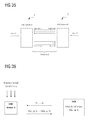
- Fig. 2 The concrete protocol for the (supposedly) secure establishment of a session key that was given in [81] is shown in Fig. 2 . It illustrates the exchange of a session key K between two parties, in this case the Bank (Party 1) on the one hand and, on the other hand, the Automated Teller Machine (ATM) with a Physical Unclonable Function (PUF) (Party 2).
- ATM Automated Teller Machine
- PAF Physical Unclonable Function
- the rest of the protocol can be understood from Fig. 2 and [81].
- the session key K exchanged in the protocol allows later "refreshment" of the challenge-response-pairs (CRPs) or the set ⁇ C i , W i , S i ⁇ stored at the bank: It can be used to transmit encrypted information between the ATM and the Bank, such as encrypted, newly measured CRPs or encrypted, newly measured tuples (C j , W j , S j '). These new CRPs/tuples (C j , W j , S j ') can then be added to the bank's CRP list/to its set ⁇ C i , W i , S i ' ⁇ .
- E&MAC K2' ( ⁇ , C 2 , W, ⁇ )
- E&MAC K3' ( ⁇ , C 3 , W, ⁇ )
- E&MAC K4' ( ⁇ , C 4 , W, ⁇ ) and may obtain C 2 , C 3 , C 4 , ... ).
- Eve can measure the PUF with the challenge C (and all other challenges C 2 , C 3 , C 4 , if applicable). She can obtain S from the measured responses, and can derive the session key K.
- the ATM can erase the measurement values M(p i , S) of the SHIC system that were used to derive K. Eve hence is unable to determine these measurement values in her second period of access, and cannot derive K herself. All previously exchanged session keys remain secure, too.
- Erasable SHIC systems therefore allow the first session key exchange protocol that remains secure if an adversary has access to the PUF twice, in particular if one access phase lies after the execution of the key exchange protocol. They hence allow secure identification applications with CRP refreshment, and significantly lowered storage requirement on the central server holding the CRP list, leading to obvious cost advantages.
- This information can be set to be a certain public key PK A that is associated with a certain party A.
- the SHIC system "hides" a public key that can be derived from the system if the set L is known.
- current PUFs can only store random bit sequences, no predetermined values.
- a certain public key today is often stored in the following way in a system that comprises a PUF: A key K is derived from the responses of the PUF; the public key is encrypted (for example by the one-time pad) with K; and the encrypted public key is is stored in a non-volatile manner in the system.
- the downside is that this requires non-volatile memory cells in the system, which can be expensive. Furthermore, these cells can be identified relatively easily, allowing read-out of the encrypted key. The method proposed above can avoid this problem.
- Alice has a sensor S with her, which makes a recording of some parameter.
- examples may include a temperature sensor, a pressure sensor, a humidity sensor, a camera, an audio-sensor, a fingerprint sensor, etc.
- Alice sends the (digital) data supposedly recorded by the sensor to Bob, and claims that the data is authentic.
- Bob could have replaced the real sensor data by any other value of her choice; she could claim a temperature of 30°C instead of the real 20°C, or send a false fingerprint, or transfer a manipulated image.
- the standard security solution to this problem would be that Bob prepares a tamper proof sensor, which is encapsulated in a secure environment. This sensor would could contain a secret key known only to the sensor and Bob. Bob hands over that specially prepared sensor to Alice. Whenever the sensor makes a recording, it authenticates the data by its key, and sends it to Bob (or Alice passes it on to Bob).
- S be a physical system
- M be a measurement apparatus.
- S is called a SHIC sensor with respect to a physical quantity Q and with respect to M if the following holds:
- M may or may not be integrated into S .
- a SHIC sensor produces an individual, hard-to-predict output that depends both on its environment and the applied measurement parameter. It must be hard to predict its output without possessing the system and actually exposing it to the quantity q. This is in strong contrast to standard SHIC systems, which are most often expected to be independent of environmental features such as temperature, etc.
- Said feature can be applied for a proof that some sensor data is authentic.
- Protocol 7.2 Proof of Authenticity of Sensor Data
- this protocol can be repeated many times for different quantities q 0 , for example if the sensor is a camera that makes a sequence of recordings.
- the first class of SHIC systems realizes the large number of possible read-out parameters by a measurement apparatus, which applies precision measurements to extract information from the object.
- a measurement apparatus which applies precision measurements to extract information from the object.
- One example for this approach is the optical implementation of a Physical One-Way Function given in [2].
- there is only a small number of independent measurement parameters in this approach each of which can be tuned with high precision and a very small stepwidth.
- combinatorial SHIC systems realize a large number of possible measurement parameters through combinatorial complexity.
- measurement schemes applied to combinatorial SHIC systems are characterized by a large number of independent parameters, each of which can only take a small number of different values. Take as an example a situation where there are 100 different measurement parameters, each of which can independently take one of 5 values. This results in an overall number of 5 100 possible different measurement vectors.
- the read-out mechanism can be expected to be less demanding and may be integrated into the object itself. This has the advantage that the combination of the object and read-out mechanism does not require any moving part, can be protected against external influences, which significantly increases the stability and repeatability of the measurement outcomes in different measurements.
- a further advantage of closely intertwining the read-out mechanism and the object is that both entities cannot be separated physically any more without noticeably altering either one.
- the possible peculiarities of the integrated read-out may even influence the response of the combined system. That means that any approach to circumvent the established read-out mechanism will deliver different results: Either because it will destroy the SHIC system or the read-out mechanism, or because it does not share the peculiarities of the original integrated read-out.
- An additional benefit of the integrated read-out mechanism is a built-in, "intrinsic" delay between subsequent read-out events. This delay can either be realized by a peripheral general clock mechanism or by designing the SHIC system itself in such a way that the system cannot be read out in arbitrarily small read-out intervals, for example because it needs a relatively long time interval in order to reach a stable equilibrium.
- combinatorial SHIC systems consists of a random distribution of electrically active junctions in form of, for example, a thin film integrated electronic device. Such a system would contain information in the form individual current-voltage characteristics of a large number of interacting electronic junctions. A preferred property of such junctions is a strongly non-linear current-voltage behavior such as for a p-n-diode or a Schottky diode.
- the complexity of the system can be scaled by the amount of junctions realized in the device matrix. Since purely electrical signals are read out, the read-out mechanism can be based on the well-established multiplex addressing used in active matrix devices.
- I-V-curve For example, take a matrix with 1000 by 1000 individual junctions, each of which has its own characteristic I-V-curve, which may depend also on the voltage applied to neighboring junctions.
- a certain row of the matrix is biased with a fixed voltage which can take N different preset values.
- the resulting current in M selected columns is detected.
- the same situation is generated at L selected different rows, each of which is biased with one of the N different voltages.
- a built in delay mechanism can be realized advantageously in this particular example by providing each junction with a suitable parallel capacitor and requiring that a valid measurement result is stable in time. Further, the delay before a stable measurement value is reached forces any adversary to wait for this period, too.
- all of the above properties of a given junction can be influenced significantly by external illumination, external magnetic or electrical fields and/or temperature.
- a further preferred property of the junctions consists in the fact that their behavior is mutually dependent on the behavior of one or more other junctions.
- the electrical properties of a given junction can be prepared during fabrication in a sufficiently random fashion, so that a sufficiently large array of junctions will be prohibitively difficult to clone or reproduce.
- the unique properties of the described system can be read out electrically in a rather simple, reliable, inexpensive and time efficient manner, as is expected from a SHIC system.
- the physical principle behind the system as described above lies in the strong dependence of miniaturized electric semiconductor heterojunctions on physical parameters such as doping, temperature, area, defects, interface states and the applied bias.
- the basic physical quantity to be detected is the current across a given junction for a particular set of bias voltages applied to that junction or to other junctions interacting with that given junction.
- the present system of junctions can be produced in such a way as to purposely increase the device to device fluctuations to a level that makes the inter device difference conveniently measurable.
- the building blocks of an integrated circuit can show several percent (10%-20%) device to device variations upon fabrication.
- One concrete implementation of the earlier, general description which can be realized with inexpensive starting material and which would hence be suitable for mass production, consists of a matrix of silicon-based p-n- or Schottky diodes produced on a glass substrate by laterally inhomogeneous deposition techniques. This inhomogeneity is important to guarantee the desired significant junction to junction variations.
- a suitable deposition technique is the laser induced, thermal or metal catalyzed crystallization of thin amorphous or nanocrystalline precursor films of silicon, silicon-germanium, etc.
- the statistical nature of nucleation and growth of individual crystallites is of primary importance for the complexity and/or the unique properties of the system.
- electrical contact can be made to individual or multiple crystallites in the form of a sandwich geometry.
- the electrical contact can either be Ohmic or of Schottky type, depending on the electrode metals and/or the doping properties of the thin semiconductor film.
- non-linear interactions between neighboring junctions can be realized.
- a suitable read-out mechanism consists of the following protocol:
- a general advantage of electrically addressable SHIC system is the ease of the read-out procedure, which can occur either in direct electrical contact or remotely via electromagnetic waves. In both cases it is possible to shield them from the external environment by Faraday cage-like constructions containing both the SHIC and the read-out system. This ensures that the detected signal indeed originates from the SHIC system, and not from an external fraudster equipped with large computing power for simulating or emulating the behaviour of the original system. For remotely readable systems even triangulation of the position of the object would be possible with a suitable antenna array to again exclude external mimic attacks.
- Another advantage of some of the above examples is that the response can be probed over a wide range in frequency, thus further enhancing the uniqueness and the resistance of the objects against counterfeiting.
- the unique physical features of an electronic device can be given by:
- the amount of structural information contained in the structure can be estimated from the number of equivalent circuit parameters needed for device description. It should be a few bytes per device instance/component. Since the number of devices in a modem integrated circuit can reach billions, this grants a very high structural information content, as desirable for SHIC systems.
- Circuit SHIC systems are hence preferrably nonlinear, or they should have so large number of inputs and outputs that even a linear system can achieve the required high input/output complexity.
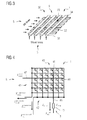
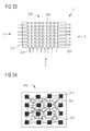
- a possible high-capacity nanoscale memory meeting the above properties for a SHIC system is a suitably designed passive crossbar structure 30, shown in Figure 3 , that shows the construction of a resistor/diode crossbar structure.
- FIG. 5 shows a read-out equivalent circuit 50 in a simplified form.
- the equivalent circuit 50 for the readout process of the crossbar memory 40 comprises the input voltage source 51 that is connected in series with a RC low-pass filter 52 comprising the input resistance R in and the net capacitance C word of the accessed word line 47, a junctional instance R junction and another RC element 53 comprising the sense resistance R sens and a capacitance C bit of the accessed bitline 48.
- a random electrical medium between the two cross bar layers (with inhomogeneities ideally on the 10 nm size scale or below, but possibly also on much larger lengthscales) can be realized, for example, by:
- the entire crossbar structure can be surrounded by a highly polarizable medium (such as an electrolyte) or capacitive trenches can be fabricated underneath the wires.
- a highly polarizable medium such as an electrolyte
- capacitive trenches can be fabricated underneath the wires.
- TFTs thin film transistors
- flash memory-like devices where the information content of the cells could be given by random manufacturing variations, for example.
- the very high information density of flash memories, combined with purposely high capacitances and / or long access paths (similar to the ones in NAND flash) can help them to fulfil the necessary security requirements.
- a further possibility is to add slow interface or oxide traps to the SHIC systems. This possibility is discussed in section 12.
- a crossbar memory used as a SHIC System (a so-called “SHIC-crossbar” or “SHIC-memory”) is different from a standard crossbar memory in the following aspects:
- junctions 43 of the circuit shown in Figure 4 are drawn by the same diode symbol, but their I ( V ) characteristics are obviously different, carrying the random structural information.
- a sense resistor 45 connected to the accessed bit line 48 which can have a low or a higher value, depending on whether current or voltage measurement is done by the sense amplifier connected to the accessed bit line 48.
- Transient behavior of the crossbar memory 40 can be modeled by adding the junction and wire-to-wire capacitances 67 to the model as shown in Figure 6 . It is required to consider the serial (Thevenin equivalent) resistance R in of the voltage generators that drive the accessed / unaccessed bit and word lines (these are omitted from Figure 6 ).
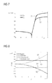
- junctions If more than a single bit of information is stored in the junctions (a plurality of curves can be distinguished in Figure 7 , not only curve 71 and 72) (analogously to multi-bit storage in modem memories), then the required measurement precision will further slow down circuit operation. Instead of reading out junctions one by one, one could compare the resistances of two randomly selected junctions. This may also provide compensation against power supply fluctuations and certain aging effects.
- One particular advantage of these processes is that they can be made compatible with modem semiconductor manufacturing technology.
- ALILE aluminum-induced layer exchange
- Figure 10 illustrates the following steps: An Al/amorphous Si (a-Si) layer stack, separated by a thin oxide film ( Figure 10 a ), is annealed at temperatures below the eutectic temperature of the Al-Si system. Annealing of the sample leads to diffusion of Si atoms into the Al layer. Crystallite formation occurs where local supersaturation of the Al with Si is achieved. In addition to that, irregularities and defects, e.g. grain boundaries of the Al, can serve as crystallization sites. As nuclei have appeared, they grow until they reach the substrate. From this point crystallites grow laterally (see Figure 10 c ) until a closed poly-Si layer has formed ( Figure 10 d ). After the process is completed, the silicon and aluminum layers exchanged their respective positions and the a-Si has been crystallized.
- a-Si Al/amorphous Si
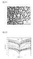
- FIG. 11 is a top-view optical microscopy image of the resulting layer where the white areas represent the crystallized silicon grains and the black surrounding the glass substrate.
- the Al remaining on top of the poly-Si layer has been removed by wet chemical etching.
- the ratio between the area covered with crystallites and the bare glass can be adjusted by the Al/Si thickness ratio.
- the size of the crystallites is determined by the annealing temperature. Since the crystallized silicon grains are Al-doped after the layer exchange process, this method results in conducting (Si-grains) and nonconducting (bare glass) regions in a truly random arrangement.
- Fully crystallized layers also reflect the randomness of their formation process and show inhomogenous conductivity.
- Poly-Si wires with a width of 1 ⁇ m - 4 ⁇ m were crystallized by the ALILE-process.
- the ALILE layer constitutes the bottom wiring.
- aluminium wires of the same size were evaporated with a mask aligned perpendicular to the Si wires.
- Figure 12 shows some measured I ( V ) curves 120 on these junctions. It is clear that the I ( V ) show sufficient randomness.
- our previously specified design targets ofN 10 10 and a read-out rate of 100 - 1000 bits per second (see above), can even be realized within a small (1 cm 2 size) active chip surface.
- Table I gives specific figures for the slow-access, memory based cryptographic SHIC system.
- the leftmost column gives the resolution or the employed fabrication technology.
- the next columns denote the number of memory units, the storage capacity of each unit, their read-out rate and the net read-out rate of the entire memory the time required for full read-out, and the planar size of the (possibly multilayered memory).
- ALILE+T refers to a technology which is currently investigated in our group, which allows to further slow down the read-out rates by using very slow semiconductor traps at the crossbar junctions. It is discussed further in section 12 of this application.
- crossbar arrays as a preferable way to implement our general idea. They reach ultimate information densities and are potentially very cost effective, since they have a very regular geometry and use only two-terminal, passive devices. Due to their simple layout, they can be produced at the limit of current nanofabrication, which gives them high security against invasive attacks and increases their security lifetime.
- USB-stick type device with dimensions of a few mm ⁇ 1 cm ⁇ 1.5 cm, which is secure for ideally up to tens of years, and which can be used for user identification, hardware identification, key exchange, and other security appliances.
- Other implementation variants tailored for specific settings can be made yet smaller and cheaper, and may thus be integrated conveniently in existing microelectronic systems.
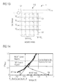
- FIG. 13 A possible wiring for such a TFT-based SHIC system 1 is shown in Figure 13 .
- the word lines 132 are connected to the TFTs' gates and the bit lines 133 to their source contacts.
- the drain contacts of all TFTs are connected over thin wires to a common voltage V COM .
- V COM common voltage
- the TFT in the upper right of the network 130 is read out.
- the parasitic current flow through the not addressed crossings is suppressed by applying a voltage V ⁇ V th to the corresponding transistor gates.
- a parallel read-out of all TFTs in one word line is prevented by the limiting current carrying capability of the wire connections between the drain contacts of the individual TFTs and V COM .
- the security of SHIC systems 1 based on the TFTs 131 relies on an inevitably low read out speed. Since the capacitances of the connecting wires are in the same range as for the SHIC systems 1 based on the crossbar memory 40, in principle the same security situation will apply. To further increase the capacitance in the system 1, the dielectric layer used in the transistor structure could be placed also between the wire connections decreasing the readout speed. Furthermore, the presence of slow traps in the insulating layer of the TFT structures also slows down the read out speed.
- non-volatile transistor - based memory cell constructions that can serve as SHIC systems with high information densities and slow read out speed.
- SHIC systems based on flash memory-like devices, where the information content of the cells could be given by random manufacturing variations, for example.
- the very high information density of flash memories, combined with purposely high capacitances and / or long access paths (similar to the ones in NAND flash) can help them to fulfil the necessary security requirements.
- a matrix array of TFTs 131 exhibiting variations in their device performances is proposed as a SHIC system 1.
- the TFT matrix offers the possibility to address the individual TFTs for read out, which minimizes leakage currents. Parallel read-out is prevented by a limited current carrying capability of the wire connections.
- the security of the system is comparable with SHICs systems 1 based on crossbar memories 40.
- the use of crystallization processes like metal-induced crystallization would also lead to high cost efficiency.
- the read-out of individual junctions can be slowed down by intentionally increasing their trap state density. Associated with these trap states, an additional capacitance is introduced to the system. By applying a certain voltage to the measured junction, the trap states have to be charged/discharged before a stable measurement value can be obtained. Depending on the corresponding time constants of the traps, which may typically lie in a range from 10 -5 s up to several hours [1301, 1302] the charge/discharge process can take considerable time frames slowing down the read out correspondingly.
- oxide traps can be occasionally introduced by high field stressing, exposure to ionizing radiation, electron avalanche injection, hole injection or Fowler-Nordheim electron injection.
- high-k dielectrics like e.g. HfO 2 , ZrO 2 , Ta 2 O 5 Certainly usually exhibit a worse quality than thermally grown SiO 2 and therefore exhibit a higher trap density.
- crossbar structures containing phase change materials can fulfill these requirements.
- the information carrying layer can be a chalcogenide-type phase change material [79].
- the phase change layer (and hence the information content of the structure) can be generally set to an essentially random value by heating the entire structure for a short time to a temperature close to the phase transition temperature, where small regions (in the size scale of a single junction) are randomly in the crystallyine or amporphous state (low or high resistance states, respectively), or by optically pre-programming [80] the device by a random-like pattern.
- the "erasure" of the information stored in one junction can then be done by applying a stronger current pulse for resetting / setting the junction, just as it is done in 'normal' phase change memories.
- This can set the information at the junction to either a predefined value or to a random value, which means that in both cases that the original information stored at the junction is no longer present.
- this procedure of setting/resetting the junction can be repeated multiple times.
- the current density required to rewrite the accessed junction are not significantly higher than the read-out current density. Since the ultimate read-out speed is determined by the finite current-carrying ability of the bit and word lines, a higher write (erase) current density would also allow a higher read-out current and faster read-out speed (which is prohibited by our construction).
- Figure 15 shows a possible random nonlinear network 150, that can also be used as system 1.
- the network 150 comprises a plurality of long range filaments 151 that are embedded in a medium 152.
- the filaments 151 can be contacted via a large number of contacts 153 that are drilled into the medium 152.
- This structure is measured by applying voltage/current at some of the contact wires and probing the current/voltage at another subset of the wires.
- the amount of extractable information should be so large ( bit) that it is practically impossible to create a look-up table for the emulation of the SHIC system behavior, even if the circuit can be accessed at a relatively fast rate.
- the medium should be a nonlinear system; it could contain long-range interconnections, to make the reconstruction of the circuit graph more difficult. Without long-range interconnections the coupling between physically distant contacts will be weak, which reduces the structure's input-output complexity.
- One preferred example of implementation is a coating layer on top of a standard silicon chip, which provides the contacts and the read-out (amplifying) circuitry.
- the coating can serve as a tamper-sensitive protective layer on top of a silicon chip, which can be used to sense any invasive tampering attempts.
- SHIC system an inhomogeneous nonlinear conducting/capacitive/inductive medium has been suggested as SHIC system, which is accessed by a large number of contacts and interrogated by static or dynamic electrical measurements.
- the structure is defined by nanometer-scale randomness and is possibly three-dimensional, providing a potentially very high security against copying and re-fabrication.
- the complexity of the internal interconnections (circuit graph) prohibits model building/emulation. Stability of a solid-state implementation is expected to be high.
- the object can be made very cheap.
- a silicon-based measurement/control circuitry is required.
- This class of electrical SHIC systems uses the dynamic behavior of nonlinear, interconnected active circuit elements (cells). The information is carried by the varying characteristics of the cells/their coupling to the neighbors. The circuit produces an output vector as a result of a dynamic pattern formation process. These devices can be viewed as a random (unique) Cellular Nonlinear Network (CNN, [14]).
- CNN Cellular Nonlinear Network
- cellular automata can be used for the design of SHIC systems with complex behavior.
- the cellular automata type implementation carries less structural information than the CNN-based device, but could be less sensitive to temperature, noise, and be more compatible with digital circuit technology.
- Each cell is characterized by a dynamical state variable, which obeys an ordinary differential equation (ODE).
- ODE ordinary differential equation
- the time derivative of the state variable depends on the y output of the neighboring cells (denoted by the k, l indices) via a the A cloning templates.
- Each cell has a bias ( z ) and inputs, which are coupled by the B template to the dynamical equation.
- the CNN behavior can be programmed by choosing appropriate templates. If only nearest neighbors are coupled, then the A and B templates are 3 ⁇ 3 matrices.
- a CNN cell which is realized from solid-state electronic components does not follow precisely the ideal CNN equations.
- Parameter deviations of the integrated circuit elements [16010] result in the deviation of templates from their nominal values. These deviations can be introduced by the fabrication process, noise, temperature, device degradation and noisy input signals [16011].
- Such mismatches represent a critical problem in scaling analog circuits in the sub-micrometer range.
- Templates which are called robust in the CNN literature, are tolerating a certain amount of mismatch.
- a CNN with not robust templates may show a unique challenge-response behavior and serve as a circuit-based SHIC system.
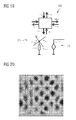
- the steady sate current distribution in the circuit shows a current intensity distribution pattern similar to interference patterns - this is illustrated by the contour plot of Figure 20 , which is the map of state variables (voltages) on the ship surface.
- Figure 20 is the map of state variables (voltages) on the ship surface.
- Figure 21 the pattern becomes more complex as the pattern of Figure 21 .
- Our simulations showed that in this design local effects (such as the change of the current or a circuit parameter in a single cell), spread strongly and globally throughout the circuit. This makes the structure dependent on relatively small fabrication variations, which is desired, and makes reverse engineering (i.e. determination of all relevant circuit parameters) extremely difficult.
- the electric field vector has only an Ez component, while the magnetic field bears the H x and Hy components.
- ⁇ x and ⁇ y are the step width of the spatial discretization.
- the 'CNN-hardware' that evolves according to the above equations (and thereby computes its solution) must be implemented as a three-layer CNN: One layer for each of the E z , H x and Hy variables. Comparing the above equations with the CNN dynamical equations, the templates can be directly determined.
- the H x and Hy layers are bi-directionally coupled to the E z layer, and there is no direct coupling between H x and Hy layers.
- the CNN If all the templates are fixed at their nominal value and the excitation vector is a single, fixedvalue cell placed at the center, then the CNN generates a wave, which is illustrated in Fig. 2a ).
- Figure 22 shows voltage distribution on chip for a mismatched Maxwell-equation solving CNN.
- the initial similarity to the non-mismatched case quickly disappears, and non-periodic nonlinear waves appear in the structure.
- the mismatches automatically lead into a non-linear regime, which is desirable in order to increase the system's complexity.
- the sigmoid-type nonlinearity has the further positive effect that it forces all the signals (circuit variables) to stay in the [-1;+1] range.
- mismatched B templates essentially are equivalent to a nonlinear, non-isotropic and optically active gain material. This 'world' is much more rich than the linear scattering effects used in [1], [2].
- the CNN model is only two-dimensional unlike the 3D token described there [1], [2].
- a more direct CNN analogy of the linear scattering PUF could also be built by placing fix zero-valued cells (obstacles, scatterers) at some (random) positions but this 'randomization strategy' realizes only lower information content and density, and is to some extent unnatural in the circuit implementation case, since there are better sources of random information and uniqueness there.
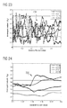
- a close-up view (from a different simulation) in Figure 24 shows that despite the 'chaotic' appearance of the curves 230 in Figure 23 , the curves 230 are changing continuously
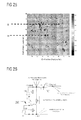
- Fig. 25 The simulations of Fig. 25 confirm that this structure sensitively responds to the change of circuit parameters (templates) as well. Changing only a single template at a particular position (denoted by B in the figure), even far away from an input (marked as In in the figure) going to alter the global behavior of the circuit detectably. These simulation results confirm that this circuit inherits the 'global sensitivity' property from optical PUFs, which make those devices so appealing. The circuit behavior also appears to be complex, as it is expected from a nonlinear dynamic system with many degrees of freedom. Work is in progress to set up machine learning experiments on simulated data to confirm that our circuit indeed withstands such types of attacks.
- Chaotic circuits are well known [16019] and several CNN templates are known to realize chaos [16020] [16021] [16022].
- the time trajectories of a chaotic system are irreproducable in a real physical environment and seem to be unsuitable as a PUF.
- a non-programmable (fixed-template) CNN cell can be built using three operational amplifiers. Additional passive elements (resistors) set the cell to cell coupling via the cloning templates, and the feedback.
- the circuit schematics is shown in Figure 26 .
- the state variable is represented by a voltage 261 of a capacitor C.
- An operational amplifier OP 1 is used for limiting the state voltage and connecting one end 262 of the capacitor C, in particular (node1), to virtual ground.
- An operational amplifier OP 2 , a resistor R 2 and a resistor R 3 work as an inverting amplifier which can realize the full nonlinear transfer characteristic to map V(state) nonlinearly to -V(output).
- the resistor R 3 is usually several times larger than resistor R 2 so as to have the operational amplifier OP 2 driven to the saturation region.
- Another inverting amplifier OP 3 is used with resistor R 5 and R 6 to provide the actual V(output).
- the weights in the A template can be controlled by changing the resistances of one of the feedback resistors, e.g. the resistor R 4 .
- the weight of the B templates are set by resistor values connecting from the neighboring cells to the node1. Kirchoff's current law applied for node1 can exactly present the CNN state equation we have discussed in Section 4. T
- CMOS operational amplifiers can be built using seven transistors so the circuit of Figure 26 requires 21 transistors.
- a state of the art CPU contains a few times ⁇ 10 7 circuit elements, an approximately 1000 ⁇ 1000 cell fixed-template CNN could be reasonable to build [16023].
- Each template carries at least a few bytes of information in its deviation from the nominal value. Obviously, some part of this information could be lost because of averaging / error correction, but the information content of the CNN-PUF should be comparable or even higher as the optical PUF of [1], [2].
- circuit-based SHIC systems An important benefit of circuit-based SHIC systems is that there are efficient circuit solutions to minimize the output instability of the circuit.
- bandgap references can provide temperature-independent voltage sources, albeit they make the circuit more complicated and slightly reduce the achievable information content per chip area.
- temperature compensation can be performed for certain templates by varying the currents and voltage levels.
- the response vector R i is read-out as a result of a stationary process. While R i depends on the internal dynamics / timing of the circuit, noise, glitches may be averaged out, increasing the stability of the circuit.
- the security is provided by the computational difficulty of reverse-engineering.
- the analog computer significantly outperforms its digital emulation and the even more extensive cryptoanalysis by digital computers seems formidably difficult. Even if model building would succeed, re-fabrication would require VLSI ASIC fabrication combined with nanolithography, which could be expensive and time consuming even for government agencies.
- the slowness of pattern formation can protect the full characterization of the device.
- the CNN-SHIC object could be relatively cheap just as today's VLSI chips.
- Figure 27 further shows elements of one particular implementation built from interconnected Chua's circuits [69], which are the classical example of chaotic circuits.
- Figure 27 shows a schematic view 271 of a Chua circuit, that is based on cells 272 which are arranged in an arrray 273, where the cell 272 is depicted by a black dot 274.
- Arrays of Chua circuits have been shown to produce complex patterns, such as spiral waves. The details of the patterns and the type of the pattern can be sensitive to the non-idealities of the circuit elements [70].
- Magnetic domains are among the most complex patterns occurring in nature and they are sensitive to atomic-scale variations of the material surface / roughness.
- magnetic domain walls can be defined artificially, e.g. writing them with an FIB (Focused Ion Beam) system on the surface of a chip.
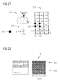
- Figure 28 show an example of a natural/random domain pattern 280 and an artificial, prestructured domain pattern 281 of a CoPt film. The example is taken from [75].
- Magnetic materials can be used in SHIC systems in two ways:
- a SHIC system where the information is carried by the unique domain patterns of a magnetic elements which change in an external magnetic fields, or the unique inductance values represented by nanoscale magnets or magnetic domains.
- Domain formation phenomena are directed by atomic-scale irregularities of the surface of the film, making characterization/re-fabrication very difficult.
- the magnetic film/nanoparticles can be fabricated cheaply and price of an integrated or external read-out circuitry is acceptable.
- SAWs Surface acoustic waves
- SAW-based SHIC object is a piezoelectric surface, with randomly positioned gratings / scratches / holes, with combinatorial excitations (microwave signals with varying amplitude / frequency) applied at chosen inputs and the electromechanical signals are picked up at the outputs, where their frequency / amplitude is measured.
- combinatorial excitations microwave signals with varying amplitude / frequency
- Figure 29 shows a device that can be used as a SHIC system 1 and is based on the propagation of surface acoustic waves.
- the device 290 comprise input transducers 291 and output transducers 292 and a disturbing structure 293 disposed between the input transducers 291 and the output transducers 292.
- the disturbing structure 293 maybe composed of gratings, scratches or holes.
- SAW-based filters are found in almost all cell phones.
- the SHIC system decribed in this section is a SHIC system whose physical uniqueness is coming from the surface irregularities of a piezoelectric film and where a complex interference pattern of surface acoustic waves can form.
- the SAW wave pattern is sensitive to irregularities on the 10 nm - 100 nm size scale and it operates on a high frequency. Due to the damping of the SAWs they are probably less secure than a optical wave propagation based SHIC system
- the device is similar to commercially available SAW filters and should be reasonably cheap.
- RFIDs radio-frequency identification devices
- the device is composed of:
- the device is build up from conductors (such as metal filaments), which act as frequency-selective antennas/resonators, the combinatorial input is directly generated by the absence or presence of this frequency in the excitation spectrum.
- conductors such as metal filaments
- the principle of operation is sketched in Figure 30 . It shows a device 300 that comprises a plurality of different frequencies elective antennas 301 on a substrate 302.
- the four intensity level per frequency band codes two bits of information for each of the frequency levels. If we assume that the antennas 301 can be excited by ten different frequencies and they are also polarization sensitive, then thirty antennas 301 can be applied in each device 300 enabling distinct combinatorial inputs.
- An example for the spectra 303 of such excitation signals is also shown in Figure 30 .
- the excited system for example, can be a random diode network measured in the frequency domain.
- This section relates to variants of the proposed SHIC systems, which are powered and interrogated by electromagnetic (e.g. radio frequency) waves and can be used as SHIC RFID's, i.e. as SHIC systems that can be interrogated remotely.
- electromagnetic e.g. radio frequency
- the security aspects are similar to those of the underlying SHIC system.
- optical system are suiteable devices for SHIC systems: their stability, the low losses occuring in transparent optical media and the intrinsic diversity and complexity of interference patterns are all desirable properties of a SHIC object.
- the SHIC object as described in the seminal paper of [2] is highly impractical as the external optical measurement apparatus is delicate and unstable.
- Our invention descibes the possibilities to build an on chip implementation of an optical SHIC system and eliminate the need for accurate optical measurements. Note that this is a non-trivial task, as the SHIC system of [2] is intrinsically a precision-measurement linear SHIC system.
- Linear optical systems cannot display combinatorial complexity, for the same reasons as linear circuits cannot (see section 7.3).
- To extract the necessary amount of structural infomation from linear systems a very large parameter space is required for the input / output variables. This large parameter space translates to a very high positioning accuracy for the laser spot.
- a common property of the above described systems is that the sources (lasers, LEDS) and the photodetectors are placed in fix position to the SHIC systems, no moving parts are necessary and the the entire system can be integrated into a monolithic circuit.
- the optical media is extremely stable against temperature variations, aging and fluctuations in optical power. This stability is more difficult to achieve in electrical systems.
- the proposed electrical / optical SHIC object can unite the beneficial properties of optical systems (i.e. stability) and electrical circuits (straightforward measurement and possibly complexity arising from nonlinear behavior).
- SHIC objects which are built as combinations of an inhomogenous, linear optical media (which produces a unique and highly complex speckle pattern) and an electrical excitation / detector array, to access it electrically.
- Figure 31 shows a device 310 that comprises an optical medium 311 that interacts with an array 312 of light sources such as laser diodes or LEDs, that can be controlled by input terminals 313.
- the optical medium 311 furher interacts with an array 314 of photo detectors such as photo diodes.
- the photo diodes of the array 314 are connected to output terminals 315.
- the linear optical media can be characterized by a scatterig matrix S , with dimensions m ⁇ n , where m is the number of excitations sources (inputs, LEDs) and n is the number of measurement points (i.e. the number of pixels in the detector array).
- S matrix carries m ⁇ n ⁇ log k ⁇ 3 ⁇ 10 14 bits of information, a sufficent amount for a SHIC system.
- This system does not exhibit combinatorical or exponential input-output complexity, such as some of our earlier suggestions and the systems discussed in section 22. Rather, its considerable complexity stems from the large number of inputs / outputs and the complexity of long range optical 'interconnections'.
- a linear optical media with an electrical LED / photodetector array, the electrical circuits exhibiting nonlinear behavior and the source / detector array being optically and possibly also electrically interconnected.
- SHIC-behavior appears due to the interplay of the high-information optical matrix and the nonlinear circuit behavior.
- the nonlinear circuit behavior enables combinatorial adressing.
- the read-out circuitry for example, a CCD array
- the read-out circuitry can be constructed to be very slow - full characterization would then take very long time and this adds an additional layer of security. It would be extremely difficult for the attacker to disassemble the monolithic circuit and install a faster photodetector array.
- a SHIC system may also a system where the information is carried by an optical media, which is accessed by an extremely large number of contacts and / or a nonlinear circuit attached to the photodiode / photodetector array or a detector array interconnected in a nonlinear way or a detector array that limits read-out speed and prevents full characterization in a reasonable amount of time.
- Such a system is also secure because the optical medium carries a well-defined amount of information in three dimensions and with an excellent long-term stability.
- LEDs / photodetectors and the electrical circuitry can be built from organic materials, then it can be reasonably cheap - solid state based implementations (with GaAs photodiodes / photodetectors) would be relatively expensive.
- the optical medium of the SHIC system should show strong nonlinear behavior, it should resist to aging / degradation and its characteristics should not exhibit strong temperature dependence. It also has to be unique (non-reproducible and different for each device instance). Scattering centers (linear / nonlinear / active / passive), randomly distimped in a transparent (linear / nonlinear / active / passive) medium can be used.
- nonlinear optical behavior occurs at relatively high intensities, which is not practical in the applications envisioned.
- resonant nonlinear effects require only moderate intensities as compared to nonresonant ones. Also gain/loss saturation effects can appear at modest intensities.
- Prominent examples are resonant plasmonic effects as resonant passive effects and random optical gain media similar to the ones used for random lasing.
- Figure 32 shows a device 320 that comprises an optical medium 321 which can be linear or nonlinear.
- an optical medium 321 which can be linear or nonlinear.
- particles 322 that are embedded in the optical medium 321.
- These particles 322 may be made from a linear or nonlinear gain medium.
- the optical medium 321 may be made from an optical gain medium.
- the particles 322 are randomly placed and oriented scatterers, which are comparable in length with the wavelength of the exciting light.
- the device may in addition contain an external pumping source that is not shown in Figure 32 . Instead of the particles 322 the optical medium may also contain other inhomogenities above the atomic scale.
- the device 320 further comprise an array of light sources 323 such as laser diodes or LEDs. Finally, the device 320 also comprises an array of photo detectors 324. The light sources 323 and the detectors 324 are accessible by a plurality of input connections 325 and output connections 326.
- Mutiple laser beams entering an active and nonlinear media through waveguides can exhibit strong and non-local crosstalk.
- the intensity / phase of the beams passing through the structure can strongly depend on the intensity / phase of the other beams entering the structure. This results in combinatorial complexity.
- Figure 33 shows a device comprising an active two-dimensional photonic crystal 330 with a plurality of waveguide inputs 331, waveguide outputs 332 and a pluraltiy of cells 333.
- this optical system shows a close analogy to the electrical SHIC system: it is also a cellular structure, the cells being nonlinear and active, but not in the electrical but the optical regime. Wiring is provided by photonic crystal waveguides.
- the most obvious choice for the cell elements are cavity nano-lasers / quantum dots.
- Organic solar cells / photodiodes are highly inhomogenous on the 100 nm / micrometer scale.
- Organic materials may make it possible to fabricate the photodiodes, photodetectors, the optical scattering media and the nonlinear circuitry from the same material system, potentially at very low costs. It is straightforward to add plasmonic nanoparticles to the organic matrix or other elements which increase nonlinearity.
- optical systems where the nonlinear and active optical materials / components give the possibility to combinatorial excitations, can also be used as SHIC systems.
- the information density can be very high with material inhomogenities in the micrometer regime and media built in 3D and he speed of the device can potentially be much faster than any of its electrical imitation.
- Tamper-sensitive SHIC systems are specially designed circuit units, which physically protect an underlying electronic system.
- the output vector of these SHIC systems should drastically and irreversibly detect any (even small / delicate) change in their physical structure.
- Passive tamper sensitive systems have inherent limitations: since in a passive device any disturbance will have a localized effect, a small 'hole' can remain unnoticed. For example, in a 1 cm size, slow-read out crossbar array, a 10 size hole would destroy only 100 bit and word lines and 99.9 percent of the information would remain intact and accessible.
- the analog cellular array is sensitive to the timing / resistances between its cells and if any change in a single cell to cell interconnection has a non-local effect, possibly changing all SHIC output vectors, then it acts as an ideal tamper-sensitive SHIC system and the underlying (protected) circuit can verify its hardware integrity with a single (or a few) measurements.
- the random optical media described in previous sections can also serve as a tamper-sensitive SHIC system.
- the photodetectors of the electrical circuit as shown in Figure 12 immediately detect any change in the interference pattern of the optical scattering medium, which inavoidably happens if the attacker breaks / drills into the optical matrix.
- SHIC systems can also be used to create tamper-sensitive devices.
- circuit-based SHIC systems allow to verify the physical integrity of the hardware of a protected circuit that can also be integrated with the SHIC system.
- the proposed device consists of:
- FIG. 35 illustrates the interconnection of the SHIC systems and their excitation scheme.
- the aim of the set-up is to prove to a third, remote party that the two depicted systems are in close proximity d to each other. To that end, they quickly exchange signals between each other, which mutually influence their behavior and their eventual outputs. If the two systems are in close proximity d, the signals can travel from one system to the other in short time, leading to different system outputs if the two systems were far remote of each other.
- the vectors Input A and Input B can serve as an initial input to the two systems. They can be randomly chosen or otherwise determined by the third party, to whom it shall be proven that the two SHIC systems are in close proximity.
- Output A and Output B are transferred to the third party, who knows the correct values for Output A and Output B for the case that the systems are in close proximity to each other, and compares them to the transferred values.
- An attacker could thus break the security of the scenario only if she could emulate the behavior of one of the systems A or B in real time at a specific location. According to their definition, this is be impossible for an interacting SHIC system.
- non-linear networks are one suited ingredient for SHIC sensors.
- callular non-linear networks with unique fabrication characteristics may be used as temperature-dependent sensors, especially if no dedicated circuit solutions (or only reduced/taylor-made solutions) are applied to delimit their temperature dependency.
- CNNs since CNNs have often been suggested in image transformations anyway, they are naturally suited as SHIC camera sensors. Tactile sensitive CNNs can also be imagined and are even currently researched, making them usable as SHIC fingerprint sensors.
- a system that comprises at least two of the features listed above and which has inner structure ensuring that a response signal is not predictable from a set of known challenge-response-pairs (CRPs) is a suitable system for security purposes.
- the system can be produced in a very compact way. Furthermore, it is easy to handle since no moving components are needed. Therefore, the system comprises also a high degree of reliability.
- the inner structure of the system may comprises a conducting network interconnecting input terminals that are used for the input signals and output terminals that are used for the output signals.
- a conducting network interconnecting input terminals that are used for the input signals and output terminals that are used for the output signals Such a signal can be produced using standard lithographic technology for the production of semiconductor devices.
- the inner structure of the system comprises a non-volatile memory-like structure with a high, random information content and with a slow access speed or low read-out rate, respectively.
- system may comprise an inner structure that includes conducting network components with non-linear current-voltage-characteristics.
- inner structure that includes conducting network components with non-linear current-voltage-characteristics.
- Another embodiment of the system comprises a cellular non-linear network that includes a plurality of cells interconnected to radiation cells.
- the temporal behavior of the state of a particular cell depends on the state and on differentials with respect to the state of neighboring cells. Also these systems can assume a degree of complexity that prevents any successful attack of an adversary.
- the system can also be realized by using wave signals as input signals generated by a plurality of input signals sources.
- output signal detectors that are associated with terminals of the inner structure are arranged for receiving wave signals as output signals.
- wavelength dependent properties of the medium can be used to create an unpredictable response signal, in particular, if the medium comprises a disordered structure.
- the medium may, for example, comprise a disordered structure made from at least two materials having different wavelengths dependent physical properties regarding the propagation of waves.
- Erasable SHIC systems can lead to strongly improved practicality in PUF-based or SHIC-system based protocols. For example, they can limit the storage volume that must be reserved for storing the response signals of previous measurements of a SHIC system/ a PUF in authentication or identification protocols. Furthermore, they allow to re-use the same SHIC system in many subsequent protocols without affecting the security of previous protocol executions. This leads to obvious economic advantages.
- a number of SHIC systems can also form a joined system if the systems are arranged for generating a response signal that depends (i) on a challenge signal applied to the joined system and (ii) the inner structure of the joined system and (iii) the physical distance of the (sub-)systems forming the the joined system.
- the response signal can be sent to a remote system, and the challenge signal can be provided by a remote system, too.
- This technique allows to prove the physical distance of the SHIC systems forming the joined system to a third party. In particular, it enables the proof that two systems are in close physical proximity (so-termed proof of colocality).
- the system can also be used for a method for security purposes.
- the method starts by requesting a measurement on the system, wherein the measurement is performed by applying a challenge signal to the system and by receiving a response signal dependent on a setting of the challenge signal and dependent on the inner structure of the system.
- the response signal is further validated by comparing the response obtained by the measurement with a response obtained from a previous measurement.
- Such a method can in particular be used for a secure cryptographic key exchange, for securing identification of entities over an insecure network and for testing labels.
- the method can further be used for performing an oblivious transfer of information or for proving colocality of two interacting systems.
- Table II shows the most important system implementations, their information complexity. We claim that our application is the first which proposes such systems and their corresponding security protocol.
- Table III shows a summary according the physical quantity representing the information and information hiding/protecting mechanism:
- Device name Information Carrier Est. information density Excitation Read-out Variants Special application Technology Remark Slow read out crossbar Serial resistance / of nonlinear junctions 1 bit / (50 nm) 2 10 1 bit /device Voltage applied to word line though decoder Optically Sense voltage measurement through decoder Several possible material system + technology Y Coating PUF Standard Silicon + nanowire by nanoimprint programmed phase change or other photosensitive layer Irregular diode network Diode nonlinearity + circuit interconnection graph device Volumetric- 1 bit / (100 nm) 2 Combinatorial, static voltage Static current / voltage measurement at selected outputs Several possible material system + technology Y Coating PUF Interacting SHIC coupies Silicon read-our circuity + spezial technology Mutual capacitances Up to 10 12 bit / device Combinatorial, pulse Time delay measurements Cellular Nonlinear Circuits Transistor thresholds, resistances, interconnection delays, mutual capacitances Few bits per square micron Few-ten bits / cell 10 8 cell /
Landscapes
- Engineering & Computer Science (AREA)
- Computer Security & Cryptography (AREA)
- Physics & Mathematics (AREA)
- Theoretical Computer Science (AREA)
- General Physics & Mathematics (AREA)
- Mathematical Physics (AREA)
- General Engineering & Computer Science (AREA)
- Signal Processing (AREA)
- Computer Hardware Design (AREA)
- Software Systems (AREA)
- Computer Networks & Wireless Communication (AREA)
- Health & Medical Sciences (AREA)
- Life Sciences & Earth Sciences (AREA)
- Biomedical Technology (AREA)
- Biophysics (AREA)
- Nanotechnology (AREA)
- Chemical & Material Sciences (AREA)
- Evolutionary Computation (AREA)
- Molecular Biology (AREA)
- Computing Systems (AREA)
- General Health & Medical Sciences (AREA)
- Electromagnetism (AREA)
- Data Mining & Analysis (AREA)
- Computational Linguistics (AREA)
- Artificial Intelligence (AREA)
- Crystallography & Structural Chemistry (AREA)
- Neurology (AREA)
- Storage Device Security (AREA)
- Data Exchanges In Wide-Area Networks (AREA)
Priority Applications (2)
| Application Number | Priority Date | Filing Date | Title |
|---|---|---|---|
| EP09175069A EP2230794A3 (fr) | 2009-03-16 | 2009-11-04 | En route vers l'intégration des systèmes SIMPL intégrés |
| PCT/EP2010/053229 WO2010105993A2 (fr) | 2009-03-16 | 2010-03-12 | Système et procédé pour applications de sécurité |
Applications Claiming Priority (3)
| Application Number | Priority Date | Filing Date | Title |
|---|---|---|---|
| EP09003763 | 2009-03-16 | ||
| EP09163641 | 2009-06-24 | ||
| EP09175069A EP2230794A3 (fr) | 2009-03-16 | 2009-11-04 | En route vers l'intégration des systèmes SIMPL intégrés |
Publications (2)
| Publication Number | Publication Date |
|---|---|
| EP2230794A2 true EP2230794A2 (fr) | 2010-09-22 |
| EP2230794A3 EP2230794A3 (fr) | 2011-10-05 |
Family
ID=41416014
Family Applications (1)
| Application Number | Title | Priority Date | Filing Date |
|---|---|---|---|
| EP09175069A Withdrawn EP2230794A3 (fr) | 2009-03-16 | 2009-11-04 | En route vers l'intégration des systèmes SIMPL intégrés |
Country Status (2)
| Country | Link |
|---|---|
| EP (1) | EP2230794A3 (fr) |
| WO (1) | WO2010105993A2 (fr) |
Cited By (25)
| Publication number | Priority date | Publication date | Assignee | Title |
|---|---|---|---|---|
| WO2013006785A3 (fr) * | 2011-07-07 | 2013-05-02 | Meng-Day Yu | Sécurité cryptographique utilisant des authentifiants flous pour des communications de dispositif et de serveur |
| US8644362B1 (en) | 2011-09-01 | 2014-02-04 | The SI Organization, Inc. | Hybrid pseudo-random noise and chaotic signal implementation for covert communication |
| WO2015088525A1 (fr) * | 2013-12-12 | 2015-06-18 | Empire Technology Development, Llc | Randomisation de temporisation de sous-unités de processeur à des fins d'amélioration de la sécurité |
| WO2016024037A1 (fr) * | 2014-08-13 | 2016-02-18 | Nokia Technologies Oy | Fonction inclonable physique |
| CN106257590A (zh) * | 2015-06-18 | 2016-12-28 | 松下知识产权经营株式会社 | 具有防篡改性的非易失性存储装置以及集成电路卡 |
| JP2017028354A (ja) * | 2015-07-16 | 2017-02-02 | 渡辺 浩志 | 電子装置ネットワーク及びチップ認証方式 |
| EP2650813A4 (fr) * | 2010-12-09 | 2017-04-26 | ICTK Co., Ltd. | Dispositif et procédé de génération d'une clé d'identification |
| WO2017153342A1 (fr) * | 2016-03-09 | 2017-09-14 | Bundesdruckerei Gmbh | Signe de sécurité pour un document et procédé pour contrôler un signe de sécurité |
| WO2017153177A1 (fr) * | 2016-03-09 | 2017-09-14 | Bundesdruckerei Gmbh | Composant électronique et procédé d'authentification d'un composant électrique à l'aide d'une fonction physique inclonable à base de nanotubes de carbone dite cnpuf |
| EP3252740A1 (fr) * | 2016-05-31 | 2017-12-06 | Schott AG | Clé optique et de cryptage d'authentification quantique protégées |
| CN107493172A (zh) * | 2016-06-13 | 2017-12-19 | 上海复旦微电子集团股份有限公司 | 无线射频认证系统及认证方法 |
| RU2660641C1 (ru) * | 2017-06-27 | 2018-07-06 | Федеральное государственное казенное военное образовательное учреждение высшего образования "Академия Федеральной службы охраны Российской Федерации" (Академия ФСО России) | Способ маскирования передаваемой информации |
| US10122537B2 (en) | 2013-12-31 | 2018-11-06 | Ictk Holdings Co., Ltd. | Apparatus and method for generating random digital value |
| CN109947588A (zh) * | 2019-02-22 | 2019-06-28 | 哈尔滨工业大学 | 一种基于支持向量回归法的NAND Flash位错误率预测方法 |
| EP3550623A1 (fr) * | 2018-04-06 | 2019-10-09 | Fraunhofer-Gesellschaft zur Förderung der angewandten Forschung e.V. | Film puf et son procédé de production |
| CN110785812A (zh) * | 2017-06-09 | 2020-02-11 | 欧普有限责任公司 | 具有类比组件的数据安全装置 |
| CN110990871A (zh) * | 2019-11-29 | 2020-04-10 | 腾讯云计算(北京)有限责任公司 | 基于人工智能的机器学习模型训练方法、预测方法及装置 |
| CN113544702A (zh) * | 2019-03-22 | 2021-10-22 | 利盟国际有限公司 | 具有预定信息层的磁性puf |
| CN113949782A (zh) * | 2021-10-13 | 2022-01-18 | 齐鲁工业大学 | 一种基于三次方忆阻器的复混沌系统数据加密方法 |
| US11301593B2 (en) | 2018-04-06 | 2022-04-12 | Fraunhofer-Gesellschaft Zur Foerderung Der Angewandten Forschung E.V. | PUF-film and method for producing the same |
| TWI762773B (zh) * | 2018-10-12 | 2022-05-01 | 日商愛德萬測試股份有限公司 | 解析裝置、解析方法及記錄有解析程式的記錄媒體 |
| US11347841B1 (en) | 2020-09-11 | 2022-05-31 | Rockwell Collins, Inc. | System and method for runtime monitoring during hash-locked remote attestation |
| US11586780B2 (en) | 2018-04-06 | 2023-02-21 | Fraunhofer-Gesellschaft Zur Foerderung Der Angewandten Forschung E.V. | PUF-film and method for producing the same |
| US11950520B2 (en) | 2018-08-23 | 2024-04-02 | The University Of Hull | Optically switchable memory |
| US12267103B2 (en) | 2020-07-16 | 2025-04-01 | British Telecommunications Public Limited Company | Electromagnetic field receiver |
Families Citing this family (41)
| Publication number | Priority date | Publication date | Assignee | Title |
|---|---|---|---|---|
| US8773886B2 (en) | 2011-08-19 | 2014-07-08 | Hewlett-Packard Development Company, L.P. | Memory array with co-planar waveguide based memory element selection |
| WO2013088939A1 (fr) * | 2011-12-13 | 2013-06-20 | 日本電気株式会社 | Dispositif de génération de données d'identification et procédé de génération de données d'identification |
| EP2763071A1 (fr) * | 2013-01-31 | 2014-08-06 | Sensirion AG | Authentification d'un capteur chimique dans un dispositif électronique portable |
| US20150134966A1 (en) * | 2013-11-10 | 2015-05-14 | Sypris Electronics, Llc | Authentication System |
| US9171810B2 (en) | 2013-11-21 | 2015-10-27 | Nxp B.V. | Electronic device incorporating a randomized interconnection layer having a randomized conduction pattern |
| WO2015105687A1 (fr) * | 2014-01-08 | 2015-07-16 | Stc.Unm | Systèmes et procédés destinés à la génération de fonctions physiquement non clonables à partir de cellules de mémoire non volatile |
| US10432409B2 (en) | 2014-05-05 | 2019-10-01 | Analog Devices, Inc. | Authentication system and device including physical unclonable function and threshold cryptography |
| US9946858B2 (en) | 2014-05-05 | 2018-04-17 | Analog Devices, Inc. | Authentication system and device including physical unclonable function and threshold cryptography |
| US9672342B2 (en) | 2014-05-05 | 2017-06-06 | Analog Devices, Inc. | System and device binding metadata with hardware intrinsic properties |
| WO2015179849A2 (fr) | 2014-05-22 | 2015-11-26 | Sypris Electronics, Llc | Système d'authentification de réseau doté d'une fonction de génération de clé dynamique |
| CN106559782B (zh) * | 2016-05-03 | 2019-11-12 | 华侨大学 | 基于混沌神经网络公钥加密算法的异构传感网加密方法 |
| US10133603B2 (en) | 2017-02-14 | 2018-11-20 | Bank Of America Corporation | Computerized system for real-time resource transfer verification and tracking |
| US10454892B2 (en) | 2017-02-21 | 2019-10-22 | Bank Of America Corporation | Determining security features for external quantum-level computing processing |
| US10447472B2 (en) | 2017-02-21 | 2019-10-15 | Bank Of America Corporation | Block computing for information silo |
| US10243976B2 (en) | 2017-02-24 | 2019-03-26 | Bank Of America Corporation | Information securities resource propagation for attack prevention |
| US10489726B2 (en) | 2017-02-27 | 2019-11-26 | Bank Of America Corporation | Lineage identification and tracking of resource inception, use, and current location |
| US10284496B2 (en) | 2017-03-03 | 2019-05-07 | Bank Of America Corporation | Computerized system for providing resource distribution channels based on predicting future resource distributions |
| US10440051B2 (en) | 2017-03-03 | 2019-10-08 | Bank Of America Corporation | Enhanced detection of polymorphic malicious content within an entity |
| US10270594B2 (en) | 2017-03-06 | 2019-04-23 | Bank Of America Corporation | Enhanced polymorphic quantum enabled firewall |
| US10437991B2 (en) | 2017-03-06 | 2019-10-08 | Bank Of America Corporation | Distractional variable identification for authentication of resource distribution |
| US10412082B2 (en) | 2017-03-09 | 2019-09-10 | Bank Of America Corporation | Multi-variable composition at channel for multi-faceted authentication |
| US11120356B2 (en) | 2017-03-17 | 2021-09-14 | Bank Of America Corporation | Morphing federated model for real-time prevention of resource abuse |
| GB2548493B (en) * | 2017-03-17 | 2018-03-28 | Quantum Base Ltd | Optical reading of a security element |
| US10440052B2 (en) | 2017-03-17 | 2019-10-08 | Bank Of America Corporation | Real-time linear identification of resource distribution breach |
| US11055776B2 (en) | 2017-03-23 | 2021-07-06 | Bank Of America Corporation | Multi-disciplinary comprehensive real-time trading signal within a designated time frame |
| US10425235B2 (en) | 2017-06-02 | 2019-09-24 | Analog Devices, Inc. | Device and system with global tamper resistance |
| US10958452B2 (en) | 2017-06-06 | 2021-03-23 | Analog Devices, Inc. | System and device including reconfigurable physical unclonable functions and threshold cryptography |
| US10426424B2 (en) | 2017-11-21 | 2019-10-01 | General Electric Company | System and method for generating and performing imaging protocol simulations |
| IL256108B (en) | 2017-12-04 | 2021-02-28 | Elbit Systems Ltd | A system and method for identifying the state of use and originality of a product |
| US11351710B2 (en) | 2018-11-05 | 2022-06-07 | Case Western Reserve University | Multilayered structures and uses thereof in security markings |
| US11194094B2 (en) * | 2018-11-05 | 2021-12-07 | Case Western Reserve University | Multilayered structures and uses thereof in security markings |
| CN112468258B (zh) * | 2019-09-06 | 2022-08-19 | 河海大学常州校区 | 一种全双工端到端自动编码器通信系统及其对抗窃听方法 |
| US11934568B2 (en) | 2019-12-12 | 2024-03-19 | Mellanox Technologies, Ltd. | Cable security |
| CN111462492B (zh) * | 2020-04-10 | 2021-03-30 | 中南大学 | 一种基于里奇流的关键路段检出方法 |
| KR102539615B1 (ko) * | 2021-11-16 | 2023-06-02 | 경희대학교 산학협력단 | 카오틱 인광 puf 및 이의 제조 방법 |
| CN114580032B (zh) * | 2022-03-02 | 2023-04-07 | 中国工程物理研究院电子工程研究所 | 一种基于原子缺陷的量子物理不可克隆函数及其制作方法 |
| CN116721722B (zh) * | 2023-06-19 | 2023-12-19 | 盛年科技有限公司 | 基于手性点阵结构力学性能数据库和数值计算方法 |
| CN118916663B (zh) * | 2024-10-11 | 2025-03-28 | 西安西电电力系统有限公司 | 阀基电子设备监视逻辑有效性验证方法及装置 |
| CN119402204B (zh) * | 2024-10-21 | 2025-09-09 | 哈尔滨工业大学 | 一种基于联盟链的智能设备安全高效认证方法 |
| CN119247985B (zh) * | 2024-12-04 | 2025-03-14 | 南京信息工程大学 | 一种完全规避禁飞区的无人机航迹规划方法 |
| CN119940695B (zh) * | 2024-12-16 | 2025-11-07 | 重庆大学 | 基于数据驱动多项式混沌展开的电氢综合能源系统可靠性评估方法 |
Citations (1)
| Publication number | Priority date | Publication date | Assignee | Title |
|---|---|---|---|---|
| US7254056B2 (en) | 2002-01-09 | 2007-08-07 | Intel Corporation | Apparatus for optically pre-programming electrically-programmable phase-change memory devices |
Family Cites Families (1)
| Publication number | Priority date | Publication date | Assignee | Title |
|---|---|---|---|---|
| WO2009024913A2 (fr) * | 2007-08-22 | 2009-02-26 | Intrinsic Id Bv | Identification de dispositifs utilisant des fonctions non clonables physiquement |
-
2009
- 2009-11-04 EP EP09175069A patent/EP2230794A3/fr not_active Withdrawn
-
2010
- 2010-03-12 WO PCT/EP2010/053229 patent/WO2010105993A2/fr not_active Ceased
Patent Citations (1)
| Publication number | Priority date | Publication date | Assignee | Title |
|---|---|---|---|---|
| US7254056B2 (en) | 2002-01-09 | 2007-08-07 | Intel Corporation | Apparatus for optically pre-programming electrically-programmable phase-change memory devices |
Non-Patent Citations (134)
| Title |
|---|
| "Cellular wave computers for nano-tera-scale technology - beyond spatial- temporal logic in million processor devices", ELECTRONICS LETTERS, vol. 43, 12 April 2007 (2007-04-12), pages 8 |
| "Doctoral Thesis", 2002, TECHNISCHE UNIVERSITAT DARMSTADT, article "S6nke Maseberg: Fail-safe Konzept fur Public Key Infrastrukturen" |
| "Secure Key Storage and Anti-Counterfeiting", 2007, SPRINGER VERLAG, article "Security with Noisy Data. Private Biometrics" |
| A. CSURGAY: "On Circuit Models of Quantum-Classical Networks", INTERNATIONAL JOURNAL OF CIRCUIT THEORY AND APPLICATIONS, vol. 35, 2007, pages 471 - 484 |
| A. DEHON ET AL.: "Nonphotolithographic nanoscale memory density prospects Nanotechnology", IEEE TRANSACTIONS ON, vol. 4, no. 2, March 2005 (2005-03-01), pages 215 - 228 |
| B. SKORIC ET AL.: "Information-theoretic analysis of capacitative physical unclonable functions", JOURNAL OF APPLIED PHYSICS, vol. 100, 2006 |
| B. SKORIC; P. TUYLIS; W. OPHEY: "Computer Science", 2005, SPRINGER, article "Robust Key Extraction from Physical Uncloneable Functions Lecture Notes" |
| BHAVNAGARWALA, A.J.; XINGHAI TANG; MEINDL, J.D.: "The impact of intrinsic device fluctuations on CMOS SPAM cell stability Solid-State Circuits", IEEE JOURNAL OF, vol. 36, no. 4, April 2001 (2001-04-01), pages 658 - 665 |
| BHAVNAGARWALA, A.J.; XINGHAI TANG; MEINDL, J.D.: "The impact of intrinsic device fluctuations on CMOS SRAM cell stability Solid-State Circuits", IEEE JOURNAL OF, vol. 36, no. 4, April 2001 (2001-04-01), pages 658 - 665 |
| BLAISE GASSEND ET AL.: "Controlled Physical Random Functions", ACSAC, 2002, pages 149 - 160 |
| BLAISE GASSEND ET AL.: "Delay-Based Circuit Authentication and Applications", SAC, 2003, pages 294 - 301 |
| BLAISE GASSEND ET AL.: "Identification and authentication of integrated circuits", CONCURRENCY - PRACTICE AND EXPERIENCE, vol. 16, no. 11, pages 1077 - 1098 |
| BLAISE GASSEND ET AL.: "Silicon physical random functions", ACM CONFERENCE ON COMPUTER AND COMMUNICATIONS SECURITY, 2002, pages 148 - 160 |
| BLAISE GASSEND: "MSc Thesis", 2003, MIT, article "Physical Random Functions" |
| BLAISE GASSEND: "Physical Random Functions Masters Thesis Computer Science and Artificial Intelligence Laboratory", February 2003, MASSACHUSETTS INSTITUTE OF TECHNOLOGY |
| BORIS SKORIC; PIM TUYLS; W. OPHEY: "Robust Key Extraction from Physical Uncloneable Functions", ACNS, 2005, pages 407 - 422 |
| BRUCE SCHNEIER: "Applied Cryptography", 1996, JOHN WILEY & SONS |
| C. CACHIN; C. CREPEAU; J. MARCIL: "Oblivious transfer with a memory-bounded receiver", PROCEEDING OF THE 39TH ANNUAL SYMPOSIUM ON FOUNDATIONS OF COMPUTER SCIENCE, 1998, pages 493 - 502 |
| C. H. BENNETT ET AL.: "Generalised Privacy Amplification", IEEE TRANSACTIONS ON INFORMATION THEORY, vol. 41, no. 6, 1995, pages 1915 - 1923 |
| C. H. BENNETT ET AL.: "Generalized privacy amplification", IEEE TRANSACTIONS ON INFORMATION THEORY, vol. 41, no. 6, 1995, pages 1915 - 1923 |
| C. JAEGER; T. ANTESBERGER; M. STUTZMANN: "Hydrogen passivation of ultra-thin low-temperature polycrystalline silicon films for electronic applications", JOURNAL OF NON-CRYSTALLINE SOLIDS, vol. 354, no. 19-25, 1 May 2008 (2008-05-01), pages 2314 - 2318 |
| CATHERINE TAYLOR CLELLAND; VIVIANA RISCA; CARTER BANCROFT: "Hiding Messages in DNA Microdots", NATURE, vol. 399, 1999, pages 533 - 534 |
| CHARLES H. BENNETT ET AL.: "Generalized Privacy Amplification", IEEE TRANSACTIONS ON INFORMATION THEORY, vol. 41, no. 6, November 1995 (1995-11-01) |
| CHARLES H. BENNETT; GILLES BRASSARD; JEAN-MARC ROBERT: "Privacy amplification by public discussion", SIAM JOURNAL ON COMPUTING, vol. 17, no. 2, April 1988 (1988-04-01) |
| CHUA, L.O. ET AL.: "CNN universal chips crank up the computing power Circuits and Devices Magazine", IEEE, vol. 12, no. 4, July 1996 (1996-07-01), pages 18 - 28 |
| CHUA, L.O.; L. YANG: "Cellular Neural Networks: Theory", IEEE TRANSACTIONS ON CIRCUITS AND SYSTEMS, vol. 35, pages 1257 - 1272 |
| COKER, A. ET AL.: "Multi-Junction Fault Tolerance Architecture for Nanoscale Crossbar Memories", IEEE TRANSACTIONS FOR NANOTECHNOLOGY |
| CSABA, G.; LUGLI, P.: "Read-out design rules for molecular cross bar architectures", IEEE |
| D. B. STRUKOV ET AL.: "The missing memristor found", NATURE, vol. 453, May 2008 (2008-05-01) |
| D. B. STRUKOV; K. K. LIKHAREV: "Defect-Tolerant Architectures for Nanoelectronic Crossbar Memories", J. NANOSCI. NANOTECHNOL., vol. 7, 2007, pages 151 - 167 |
| D. BLAISE GASSEND ET AL., SILICON PHYSICAL RANDOM FUNCTIONS CSC, 18 November 2002 (2002-11-18) |
| D.W. BAUDER: "An Anti-Counterfeiting Concept for Currency Systems. Research report PTK-11990", SANDIA NATIONAL LABS, 1983 |
| DAIHYUN LIM ET AL.: "Extracting secret keys from integrated circuits", IEEE TRANS. VLSI SYST., vol. 13, no. 10, 2005, pages 1200 - 1205 |
| DAIHYUN LIM ET AL.: "Extracting secret keys from integrated circuits, Very Large Scale Integration (VLSI) Systems", IEEE TRANSACTIONS ON, vol. 13, no. 10, October 2005 (2005-10-01), pages 1200 - 1205 |
| DAIHYUN LIM ET AL.: "Extracting secret keys from integrated circuits, Very Large Scale Integration (VLSI) Systems", IEEE TRANSACTIONS, vol. 13, no. 10, October 2005 (2005-10-01), pages 1200 - 1205 |
| DAIHYUN LIM: "MSc Thesis", 2004, MIT, article "Extracting Secret Keys from Integrated Circuits" |
| DARKO KIROVSKI: "A Point-Set Compression Heuristic for Fiber-Based Certificates of Authenticity", DCC, 2005, pages 103 - 112 |
| DARKO KIROVSKI: "Point Compression for Certificates of Authenticity", DATA COMPRESSION CONFERENCE, 2004, pages 545 |
| DARKO KIROVSKI: "Toward an automated verification of certificates of authenticity", ACM CONFERENCE ON ELECTRONIC COMMERCE, 2004, pages 160 - 169 |
| DAVID DEUTSCH: "Quantum Theory, the Church-Turing Principle and the Universal Quantum Computer", PROC. ROYAL SOC., vol. 400, 1985, pages 96 - 117 |
| DE GRAAF, C. ET AL.: "A novel high-density low-cost diode programmable read only memory", ELECTRON DEVICES MEETING, 8 December 1996 (1996-12-08), pages 189 - 192 |
| DE GRAAF, C. ET AL.: "A novel high-density lowcost diode programmable read only memory", ELECTRON DEVICES MEETING, 8 December 1996 (1996-12-08), pages 189 - 192 |
| DEEPAK VIJAYWARGI; DAVE LEWIS; DARKO KIROVSKI: "Optical DNA", FINANCIAL CRYPTOGRAPHY, 2009, pages 222 - 229 |
| DOUGLAS R; STINSON: "Cryptography: Theory and Practice", 2005, CRC PRESS |
| E. H. NICOLLIAN; A. GOETZBERGER: "The Si-Si02 Interface-Electrical properties as determined by the MIS Conductance Technique", BELL SYST. TECH. J., vol. 46, 1967, pages 1055 |
| E. S. P. LEONG; S. F. YU; S. P. LAU: "Directional edge-emitting UV random laser diodes", APPL. PHYS. LETT., vol. 89, 2006, pages 221109 |
| ERIK ANDERSON ET AL.: "Key Management and Encryption under the Bounded Storage Model", SANDIA REPORT SAND2005-6979, November 2005 (2005-11-01) |
| FRANK: "On the Foundations of Physical Unclonable Functions", CRYPTOLOGY EPRINT ARCHIVE, REPORT NO. 2009/277, 2009, Retrieved from the Internet <URL:http://eprint.iacr.org/index.html> |
| G. EDWARD SUH ET AL.: "AEGIS: architecture for tamper-evident and tamper-resistant processing", ICS, 2003, pages 160 - 171 |
| G. EDWARD SUH ET AL.: "Design and Implementation of the AEGIS Single-Chip Secure Processor Using Physical Random Functions", ISCA, 2005, pages 25 - 36 |
| G. EDWARD SUH; SRINIVAS DEVADAS: "Physical Unclonable Functions for Device Authentication and Secret Key Generation", PROCEEDINGS OF THE 44TH DESIGN AUTOMATION CONFERENCE (DAC), 2007 |
| G. F. CEROFOLINI ET AL.: "Mascolo, A hybrid approach to nanoelectronics", NANOTECHNOLOGY, vol. 16, 2005, pages 1040 - 1047 |
| GERALD DE JEAN; DARKO KIROVSKI, CERTIFYING AUTHENTICITY USING RF WAVES, Retrieved from the Internet <URL:http://research.microsoft.com/users/darkok> |
| GERALD DE JEAN; DARKO KIROVSKI, RADIO FREQUENCY CERTIFICATES OF AUTHENTICITY, Retrieved from the Internet <URL:http://research.microsoft.com/users/darkok> |
| GERALD DEJEAN; DARKO KIROVSKI: "RF-DNA: Radio-Frequency Certificates of Authenticity", CHES, 2007, pages 346 - 363 |
| GERALD DEJEAN; DARKO KIROVSKI: "RF-DNA: Radio-Frequency Certificates of Authenticity", vol. 4727, 2007, SPRINGER, article "RF-DNA: Radio-Frequency Certificates of Authenticity" |
| J. A. BUCHMANN: "Introduction to Cryptography", 2003, SPRINGER |
| J. D. JACKSON: "Classical electrodynamics", 1998, WILEY |
| JAMES D. R. BUCHANAN ET AL.: "Fingerprinting documents and packaging", NATURE, vol. 236, 2005, pages 475 |
| JOE KILIAN: "Founding crytpography on oblivious transfer", PROCEEDINGS OF THE TWENTIETH ANNUAL ACM SYMPOSIUM ON THEORY OF COMPUTING, 1988, pages 20 - 31 |
| JOHNSON, M. ET AL.: "512-Mb PROM with a three-dimensional array of diode/antifuse memory cells, Solid-State Circuits", IEEE JOURNAL OF, vol. 3 8, no. 11, November 2003 (2003-11-01), pages 1920 - 1928 |
| JOHNSON, M. ET AL.: "512-Mb PROM with a threedimensional array of diodelantifuse memory cells, Solid-State Circuits", IEEE JOURNAL OF, vol. 38, no. 11, November 2003 (2003-11-01), pages 1920 - 1928 |
| JORGE GUAJARDO ET AL.: "CHES", vol. 4727, 2007, SPRINGER LNCS, article "FPGA Intrinsic PUFs and Their Use for IP Protection", pages: 63 - 80 |
| KENNEDY, M.P.: "Three steps to chaos. II: A Chua's circuit primer", IEEE TRANSACTIONS ON CIRCUITS AND SYSTEMS I: FUNDAMENTAL THEORY AND APPLICATIONS, vol. 40, no. 10, October 1993 (1993-10-01), pages 657 - 674 |
| KONRAD ZUSE; K. ZUSE: "Rechnender Raum, Schriften zur Datenverarbeitung", 1969, VIEWEG & SOHN, article "Calculating space. MIT Technical translation" |
| KUMAR, S.S. ET AL.: "Extended abstract: The butterfly PUF protecting IP on every FPGA", HARDWARE-ORIENTED SECURITY AND TRUST, 2008, 9 June 2008 (2008-06-09), pages 67 - 70 |
| L. O. CHUA: "CNN: A paradigm for complexity", June 1998, WORLD SCIENTIFIC PUB. CO |
| L. O. CHUA; T. ROSKA: "Cellular Neural Networks and Visual Computing: Foundations and Applications", 2005, CAMBRIDGE UNIVERSITY PRESS |
| L. O. CHUA; T. ROSKA: "Cellular Neural Networks and Visual Computing: Foundations and Applications", 2005, CAMBRIDGE UNIVERSITY PRESS, article "Cellular Neural Networks and Visual Computing: Foundations and Applications" |
| L. P. TROMBETTA; F. J. FEIGL; J. R. ZETO: "Positive charge generation in metal- oxide-semiconductor capacitors", J. APPL. PHYS., vol. 69, 1991, pages 4 |
| LAI, S.: "Current status of the phase change memory and its future", ELECTRON DEVICES MEETING, 2003. IEDM '03 TECHNICAL DIGEST. IEEE INTERNATIONAL, 8 December 2003 (2003-12-08), pages 10.1.1 - 10.1.4 |
| LIM, D.: "Extracting secret keys from integrated circuits, MSc thesis, MIT, 2004, or variants thereof", THE PARAMETERS USED IN THE RESPECTIVE MACHINE LEARNING ALGORITHMS ARE MOSTLY STANDARD PARAMETERS |
| LIM, D.: "MSc thesis", 2004, MIT, article "Extracting secret keys from integrated circuits" |
| M. BECHERER ET AL.: "Magnetic Ordering of Focused-lon-Beam Structured Cobalt-Platinum Dots", FIELD-COUPLED COMPUTING IEEE TRANSACTIONS ON NANOTECHNOLOGY, 2008 |
| M. ERCSEY-RAVASZ; T. ROSKA; Z. NEDA: "Cellular Neural Networks for NP-Hard Optimization EURASIP Journal on Advances", SIGNAL PROCESSING, vol. 2009, pages 64697 |
| M. G'OMEZ-GESTEIRA ET AL.: "Experimental Chua's Circuit Arrays As an Autowave Simulator", IEEE TRANSACTIONS ON CIRCUITS AND SYSTEMS---I: FUNDAMENTAL THEORY AND APPLICATIONS, vol. 46, no. 4, April 1999 (1999-04-01) |
| M. GOMEZ-GESTEIRA ET AL.: "Experimental-Chua's Circuit Arrays As an Autowave Simulator", IEEE TRANSACTIONS ON CIRCUITS AND SYSTEMS-1: FUNDAMENTAL THEORY AND APPLICATIONS, vol. 46, no. 4, April 1999 (1999-04-01) |
| M. HALLERMANN: "Characterization ofPhotonic Crystal Nanostructures for Molecular Cryptography", BACHELOR THESIS, 2005 |
| M.M. ZIEGLER; M. R. STAN: "Design and analysis of crossbar circuits for molecular nanoelectronics Nanotechnology, 2002. IEEE-NANO 2002", PROCEEDINGS OF THE 2002 2ND IEEE CONFERENCE ON, 2002, pages 323 - 327 |
| M.M. ZIEGLER; M.R. STAN: "CMOSlnano co-design for crossbar-based molecular electronic systems", NANOTECHNOLOGY, IEEE TRANSACTIONS ON, vol. 2, no. 4, December 2003 (2003-12-01), pages 217 - 230 |
| MACIEJ J. OGORZALEK ET AL.: "Chaotic Waves and Spatio-Temporal Patterns in Large Arrays of Doubly-Coupled Chua' s Circuits", IEEE TRANSACTIONS ON CIRCUITS AND SYSTEMS-I: FUNDAMENTAL THEORY AND APPLICATIONS, vol. 42, no. 10, October 1995 (1995-10-01) |
| MAEDA, S. ET AL.: "An artificial fingerprint device (AFD) module using poly-Si thin film transistors with logic LSI compatible process for built-in security Electron Devices Meeting, 2001", IEDM TECHNICAL DIGEST. INTERNATIONAL, 2001, pages 34.5.1 - 34.5.4 |
| MAEDA, S. ET AL.: "An artificial fingerprint device (AFD): a study of identification number applications utilizing characteristics variation of polycrystalline silicon TFTs, Electron Devices", IEEE TRANSACTIONS ON, vol. 50, no. 6, June 2003 (2003-06-01), pages 1451 - 1458 |
| MICHELE PRA ET AL.: "Simulation ofZnO diodes for application in non-volatile crossbar memories", JOURNAL OF COMPUTATIONAL ELECTRONICS |
| MICHELE PRA; GYORGY CSABA: "Journal of computational electronics", article "Christoph Erlen and Paolo Lugli: Simulation of ZnO diodes for application in non-volatile crossbar memories" |
| O. NAST ET AL.: "Aluminum-induced crystallization of amorphous silicon on glass substrates above and below the eutectic temperature", APPL. PHYS. LETT., vol. 73, 1998, pages 3214 |
| P. TUYLS; B. SKORIC: "Security, Privacy and Trust in Modern Data Management", 2007, SPRINGER, article "Strong Authentication with Physical Unclonable Functions" |
| PAPPU, R. ET AL.: "Physical One-Way Functions", SCIENCE, vol. 297, 20 September 2002 (2002-09-20), pages 2026 - 2030 |
| PIM TUYLS ET AL.: "CHES", vol. 4249, 2006, SPRINGER LNCS, article "Read-Proof Hardware from Protective Coatings", pages: 369 - 383 |
| PIM TUYLS ET AL.: "Computer Science", 2006, SPRINGER BERLIN/HEIDELBERG, article "Read-Proof Hardware from Protective Coatings Lecture Notes" |
| PIM TUYLS ET AL.: "Information-Theoretic Security Analysis of Physical Uncloneable Functions", FINANCIAL CRYPTOGRAPHY, 2005, pages 141 - 155 |
| PIM TUYLS ET AL.: "Read-Proof Hardware from Protective Coatings", CHES, 2006, pages 369 - 383 |
| PIM TUYLS ET AL.: "Read-proofhardwarefrom protective coatings", CHES, 2006, pages 369 - 383 |
| PIM TUYLS: "Grey-Box Cryptography: Physical Unclonable Functions", ESAS, 2006, pages 3 - 5 |
| PIM TUYLS; LEJLA BATINA: "RFID-Tags for Anti-counterfeiting", CT-RSA, 2006, pages 115 - 131 |
| R. JANSSEN ET AL.: "Optical and electrical properties of doped amorphous silicon suboxides Phys", REV. B, vol. 60, 1999, pages 13561 - 13572 |
| R. JANSSEN ET AL.: "Optical and electrical properties of doped amorphous silicon suboxides", PHYS. REV. B, vol. 60, 1999, pages 13561 - 13572 |
| R. PAPPU ET AL.: "Physical One-Way Functions", SCIENCE, vol. 297, 20 September 2002 (2002-09-20), pages 2026 - 2030 |
| R. PAPPU ET AL.: "Physical One-Way functions", SCIENCE, vol. 297, no. 5589, September 2002 (2002-09-01), pages 2026 - 2030 |
| R. PAPPU: "PhD Thesis", MIT, article "Physical One-Way Functions" |
| R. RENNER; S. WOLF: "Simple and Tight Bounds for Information Reconciliation and Privacy Amplification", ASIACRYPT, 2005, pages 199 - 216 |
| ROLF LANDAUER: "Information is Physical", PHYSICS TODAY, 1991, pages 23 - 29 |
| ROSKA, T.; CHUA, L.O.: "The CNN universal machine: An analogic array computer", CIRCUITS AND SYSTEMS II: IEEE TRANSACTIONS ON ANALOG AND DIGITAL SIGNAL PROCESSING, vol. 40, no. 3, March 1993 (1993-03-01), pages 163 - 173 |
| ROSS ANDERSON: "Security Engineering", 2001, WILEY |
| S. D. BROTHERTON: "Polycrystalline silicon thin film transistors", SEMICOND. SCI. TECHNOL., vol. 10, 1995, pages 721 - 738 |
| S. F. NELSON ET AL.: "Temperature-independent transport in high-mobility pentacene transistors", APPL. PHYS. LETT., vol. 72, 1998, pages 1854 |
| S. K. DEY; R. ZULEEG: "Processing and parameters of sol-gel PZT thinfilms for GaAs memory applications", FERROELOECTRICS, vol. 112, 1990, pages 309 - 319 |
| S. SKOROBOGATOV: "PhD Thesis", 2005, CAMBRIDGE UNIVERSITY, article "Semi-invasive attacks -- A new approach to hardware security analysis" |
| S. WOLFRAM: "Statistical mechanics of cellular automata Rev", MOD. PHYS., vol. 55, 1983, pages 601 - 644 |
| S. WOLFRAM: "Statistical mechanics of cellular automata", REV. MOD. PHYS., vol. 55, 1983, pages 601 - 644 |
| S. XAVIER-DE-SOUZA ET AL.: "Chip-Specific Robustness", IEEE TRANS. ON CIRCUITS AND SYSTEMS - 1, vol. 51, no. 5, 2004, pages 892 - 902 |
| SERPICO, C.; SETTI, G.; THIRAN, P.: "Advances in intelligent Systems", vol. 41, 1997, IOS PRESS, article "Analogies between cellular neural networks and partial differential equations", pages: 157 - 162 |
| STEFAN WOLF; JÜRG WULLSCHLEGER: "EUROCRYPT", vol. 4004, 2006, SPRINGER LECTURE NOTES IN COMPUTER SCIENCE, article "Oblivious Transfer Is Symmetric", pages: 222 - 232 |
| T. ANTESBERGER ET AL.: "Structural and electronic properties of ultrathin polycrystalline Si layers on glass prepared by aluminum-induced layer exchange", APPL. PHYS. LETT., vol. 91, 2007, pages 201909 |
| T. KOBORI; T. MANUYAMA; T. HOSHINO: "A Cellular Automata System with FPGA", PROCEEDINGS OF THE THE 9TH ANNUAL IEEE SYMPOSIUM ON FIELD-PROGRAMMABLE CUSTOM COMPUTING MACHINES |
| T. M. COVER: "Enumerative Source Encoding", IEEE TRANSACTIONS ON INFORMATION THEORY, vol. 19, no. 1, 1973, pages 73 - 77 |
| T. ROSKA ET AL.: "Simulating nonlin ear waves and partial differential equations via CNN-Part I: Basic techniques", IEEE TRANSACTION ON CIRCUITS AND SYSTEMS-1, vol. 42, 1995, pages 807 - 815 |
| T.-F. CHEN ET AL.: "A novel four-mask-processed poly-Si TFT fabricated using excimer laser crystallization of an edge-thickened a-Si active island", IEEE ELECTRON. DEV. LETT., vol. 25, 2004, pages 396 |
| THE WORLD ECONOMIC FORUM, 2004 |
| U. MAURER: "Conditionally perfect secrecy and a provably secure randomized cipher", JOURNAL OF CRYPTOLOGY, vol. 5, no. 1, 1992, pages 53 - 66 |
| U. RIIHRMAIR; J. J. FINLEY; M. STUTZMANN: "Unique Objects and Their Applications to Cryptography and Security", REPORT, 2006 |
| U. RÜHRMAIR, SIMPL OBJECTS AND THEIR APPLICATIONS, 2007 |
| U. RÜHRMAIR: "SHIC Objects and Their Applications to Cryptography and Security", REPORT, 2007 |
| UELI M. MAURER: "Secure multi-party computation made simple", DISCRETE APPLIED MATHEMATICS, vol. 154, no. 2, 2006, pages 370 - 381 |
| UELI MAURER: "Journal of Cryptology", vol. 5, 1992, SPRINGER, article "Conditionally-perfect secrecy and a provably-secure randomized cipher", pages: 1 |
| VITTOZ, E.A.: "The Design of High-Performance Analog Circuits on Digital CMOS Chips, Solid-State Circuits", IEEE JOURNAL OF, vol. 20, no. 3, June 1985 (1985-06-01), pages 657 - 665 |
| WILLIAM H. PRESS ET AL.: "Numerical Recipes in C: The Art of Scientific Computing", 30 October 1992, CAMBRIDGE UNIVERSITY PRESS |
| WOLFGANG POROD; HENRY K. HARBURY; CRAIG S. LENT: "Study of Wave Phenomena in Physically- Coupled Device Arrays Using the Helmholtz Equation as a Model", PHYSICS AND COMPUTATION - PHYSCOMP96, November 1996 (1996-11-01) |
| X. HUANG; A. A. MARADUDIN: "Propagation of surface acoustic waves across random gratings Phys", REV. B, vol. 36, 1987, pages 7827 - 7839 |
| Y. CHEN ET AL.: "Nanoscale molecular-switch crossbar circuits", NANOTECHNOLOGY, vol. 14, 2003, pages 462 - 468 |
| Y. DODIS; L. REYZIN; A. SMITH: "Fuzzy Extractors: How to Generate Strong Keys from Biometrics and Other Noisy Data", EUROCRYPT, 2004, pages 523 - 540 |
| Y.Z. DING ET AL.: "Constant-Round Oblivious Transfer in the Bounded Storage Model", JOURNAL OF CRYPTOLOGY, 2007 |
| YONG CHEN ET AL.: "Nanoscale molecular-switch crossbar Circuits", NANOTECHNOLOGY, vol. 14, 2003, pages 462 - 468 |
| ZOU, F.; J.A. NOSSEK: "A chaotic attractor with cellular neural networks", IEEE TRANSACTION ON CIRCUITS AND SYSTEMS, vol. 38, 1991, pages 811 - 812 |
Cited By (53)
| Publication number | Priority date | Publication date | Assignee | Title |
|---|---|---|---|---|
| EP3518457A3 (fr) * | 2010-12-09 | 2019-08-07 | ICTK Holdings Co., Ltd. | Dispositif et procédé de génération d'une clé d'identification |
| US10235540B2 (en) | 2010-12-09 | 2019-03-19 | Ictk Holdings Co., Ltd. | Apparatus and method for generating identification key |
| US10769309B2 (en) | 2010-12-09 | 2020-09-08 | Ictk Holdings Co., Ltd | Apparatus and method for generating identification key |
| EP2650813A4 (fr) * | 2010-12-09 | 2017-04-26 | ICTK Co., Ltd. | Dispositif et procédé de génération d'une clé d'identification |
| US8762723B2 (en) | 2011-07-07 | 2014-06-24 | Verayo, Inc. | Cryptographic security using fuzzy credentials for device and server communications |
| WO2013006785A3 (fr) * | 2011-07-07 | 2013-05-02 | Meng-Day Yu | Sécurité cryptographique utilisant des authentifiants flous pour des communications de dispositif et de serveur |
| US8644362B1 (en) | 2011-09-01 | 2014-02-04 | The SI Organization, Inc. | Hybrid pseudo-random noise and chaotic signal implementation for covert communication |
| WO2015088525A1 (fr) * | 2013-12-12 | 2015-06-18 | Empire Technology Development, Llc | Randomisation de temporisation de sous-unités de processeur à des fins d'amélioration de la sécurité |
| US9419993B2 (en) | 2013-12-12 | 2016-08-16 | Empire Technology Development Llc | Randomization of processor subunit timing to enhance security |
| US10771268B2 (en) | 2013-12-31 | 2020-09-08 | Ictk Holdings Co., Ltd | Apparatus and method for generating random digital value |
| US10122537B2 (en) | 2013-12-31 | 2018-11-06 | Ictk Holdings Co., Ltd. | Apparatus and method for generating random digital value |
| US10491407B2 (en) | 2014-08-13 | 2019-11-26 | Nokia Technologies Oy | Physical unclonable function |
| WO2016024037A1 (fr) * | 2014-08-13 | 2016-02-18 | Nokia Technologies Oy | Fonction inclonable physique |
| CN106257590B (zh) * | 2015-06-18 | 2021-03-30 | 新唐科技日本株式会社 | 具有防篡改性的非易失性存储装置以及集成电路卡 |
| CN106257590A (zh) * | 2015-06-18 | 2016-12-28 | 松下知识产权经营株式会社 | 具有防篡改性的非易失性存储装置以及集成电路卡 |
| EP3118770A3 (fr) * | 2015-07-16 | 2017-04-12 | Hiroshi Watanabe | Unité de réseau d'appareils électroniques, réseau de tels appareils et procédé d'identification de puce |
| JP2017028354A (ja) * | 2015-07-16 | 2017-02-02 | 渡辺 浩志 | 電子装置ネットワーク及びチップ認証方式 |
| WO2017153177A1 (fr) * | 2016-03-09 | 2017-09-14 | Bundesdruckerei Gmbh | Composant électronique et procédé d'authentification d'un composant électrique à l'aide d'une fonction physique inclonable à base de nanotubes de carbone dite cnpuf |
| WO2017153342A1 (fr) * | 2016-03-09 | 2017-09-14 | Bundesdruckerei Gmbh | Signe de sécurité pour un document et procédé pour contrôler un signe de sécurité |
| US11212120B2 (en) | 2016-05-31 | 2021-12-28 | Schott Ag | Optical key protected authentication and encryption |
| WO2017207219A1 (fr) * | 2016-05-31 | 2017-12-07 | Schott Ag | Authentification et cryptage quantiques protégés par des clés optiques |
| EP3252740A1 (fr) * | 2016-05-31 | 2017-12-06 | Schott AG | Clé optique et de cryptage d'authentification quantique protégées |
| CN107493172B (zh) * | 2016-06-13 | 2020-07-17 | 上海复旦微电子集团股份有限公司 | 无线射频认证系统及认证方法 |
| CN107493172A (zh) * | 2016-06-13 | 2017-12-19 | 上海复旦微电子集团股份有限公司 | 无线射频认证系统及认证方法 |
| KR20230137476A (ko) * | 2017-06-09 | 2023-10-04 | 오피이 엘엘씨 | 아날로그 콤포넌트를 갖는 데이터 보안 장치 |
| US11699361B2 (en) | 2017-06-09 | 2023-07-11 | Ope, Llc | Data security apparatus and method using constant optical signal input to analog component |
| JP2020525863A (ja) * | 2017-06-09 | 2020-08-27 | オーピーイー エルエルシー | アナログコンポーネントを備えたデータセキュリティ装置 |
| US12380813B2 (en) | 2017-06-09 | 2025-08-05 | OPë, LLC | Control circuitry for data security apparatus |
| EP4421661A3 (fr) * | 2017-06-09 | 2024-11-27 | Ope LLC | Appareil de sécurité de données avec composant analogique |
| CN110785812B (zh) * | 2017-06-09 | 2023-12-01 | 欧普有限责任公司 | 具有类比组件的数据安全装置 |
| EP3635725A4 (fr) * | 2017-06-09 | 2021-03-03 | Ope LLC | Appareil de sécurité de données pourvu d'un composant analogique |
| KR20200016365A (ko) * | 2017-06-09 | 2020-02-14 | 오피이 엘엘씨 | 아날로그 콤포넌트를 갖는 데이터 보안 장치 |
| US11004360B2 (en) | 2017-06-09 | 2021-05-11 | OPe LLC | Data security apparatus with analog component |
| CN110785812A (zh) * | 2017-06-09 | 2020-02-11 | 欧普有限责任公司 | 具有类比组件的数据安全装置 |
| RU2660641C1 (ru) * | 2017-06-27 | 2018-07-06 | Федеральное государственное казенное военное образовательное учреждение высшего образования "Академия Федеральной службы охраны Российской Федерации" (Академия ФСО России) | Способ маскирования передаваемой информации |
| EP3550623A1 (fr) * | 2018-04-06 | 2019-10-09 | Fraunhofer-Gesellschaft zur Förderung der angewandten Forschung e.V. | Film puf et son procédé de production |
| US11301593B2 (en) | 2018-04-06 | 2022-04-12 | Fraunhofer-Gesellschaft Zur Foerderung Der Angewandten Forschung E.V. | PUF-film and method for producing the same |
| US11586780B2 (en) | 2018-04-06 | 2023-02-21 | Fraunhofer-Gesellschaft Zur Foerderung Der Angewandten Forschung E.V. | PUF-film and method for producing the same |
| US11889004B2 (en) | 2018-04-06 | 2024-01-30 | Fraunhofer-Gesellschaft Zur Foerderung Der Angewandten Forschung E.V. | PUF-film and method for producing the same |
| US11411748B2 (en) | 2018-04-06 | 2022-08-09 | Fraunhofer-Gesellschaft Zur Foerderung Der Angewandten Forschung E.V. | PUF-film and method for producing the same |
| US11950520B2 (en) | 2018-08-23 | 2024-04-02 | The University Of Hull | Optically switchable memory |
| TWI762773B (zh) * | 2018-10-12 | 2022-05-01 | 日商愛德萬測試股份有限公司 | 解析裝置、解析方法及記錄有解析程式的記錄媒體 |
| CN109947588A (zh) * | 2019-02-22 | 2019-06-28 | 哈尔滨工业大学 | 一种基于支持向量回归法的NAND Flash位错误率预测方法 |
| CN109947588B (zh) * | 2019-02-22 | 2021-01-12 | 哈尔滨工业大学 | 一种基于支持向量回归法的NAND Flash位错误率预测方法 |
| CN113544702A (zh) * | 2019-03-22 | 2021-10-22 | 利盟国际有限公司 | 具有预定信息层的磁性puf |
| US11951759B2 (en) * | 2019-03-22 | 2024-04-09 | Lexmark International, Inc. | Magnetic PUF with predetermined information layer |
| US20220410612A1 (en) * | 2019-03-22 | 2022-12-29 | Lexmark International, Inc. | Magnetic PUF with Predetermined Information Layer |
| CN110990871A (zh) * | 2019-11-29 | 2020-04-10 | 腾讯云计算(北京)有限责任公司 | 基于人工智能的机器学习模型训练方法、预测方法及装置 |
| CN110990871B (zh) * | 2019-11-29 | 2023-04-07 | 腾讯云计算(北京)有限责任公司 | 基于人工智能的机器学习模型训练方法、预测方法及装置 |
| US12267103B2 (en) | 2020-07-16 | 2025-04-01 | British Telecommunications Public Limited Company | Electromagnetic field receiver |
| US11347841B1 (en) | 2020-09-11 | 2022-05-31 | Rockwell Collins, Inc. | System and method for runtime monitoring during hash-locked remote attestation |
| CN113949782B (zh) * | 2021-10-13 | 2024-03-29 | 齐鲁工业大学 | 一种基于三次方忆阻器的复混沌系统数据加密方法 |
| CN113949782A (zh) * | 2021-10-13 | 2022-01-18 | 齐鲁工业大学 | 一种基于三次方忆阻器的复混沌系统数据加密方法 |
Also Published As
| Publication number | Publication date |
|---|---|
| EP2230794A3 (fr) | 2011-10-05 |
| WO2010105993A2 (fr) | 2010-09-23 |
| WO2010105993A3 (fr) | 2011-12-08 |
Similar Documents
| Publication | Publication Date | Title |
|---|---|---|
| EP2230794A2 (fr) | En route vers l'intégration des systèmes SIMPL intégrés | |
| Gao et al. | Physical unclonable functions | |
| Gao et al. | Emerging physical unclonable functions with nanotechnology | |
| Al-Meer et al. | Physical unclonable functions (PUF) for IoT devices | |
| Ning et al. | Physical unclonable function: Architectures, applications and challenges for dependable security | |
| Chang et al. | A retrospective and a look forward: Fifteen years of physical unclonable function advancement | |
| Joshi et al. | Everything you wanted to know about PUFs | |
| Pang et al. | Memristors for hardware security applications | |
| Gao et al. | Memristive crypto primitive for building highly secure physical unclonable functions | |
| US11218316B2 (en) | Secure computing hardware apparatus | |
| Jiang et al. | A provable key destruction scheme based on memristive crossbar arrays | |
| Rajendran et al. | Application of resistive random access memory in hardware security: A review | |
| Delvaux et al. | Security analysis of PUF-based key generation and entity authentication | |
| Mazady et al. | Memristor PUF—A security primitive: Theory and experiment | |
| Rose et al. | A write-time based memristive PUF for hardware security applications | |
| Ibrahim et al. | Memristor-based PUF for lightweight cryptographic randomness | |
| US9660806B2 (en) | Carbon nanotube array for cryptographic key generation and protection | |
| Rostami et al. | Quo vadis, PUF?: Trends and challenges of emerging physical-disorder based security | |
| Kim et al. | Investigation of physically unclonable functions using flash memory for integrated circuit authentication | |
| TWI874383B (zh) | 用於確定裝置的識別符值的方法、電腦可讀取媒體、控制器及用於確定其識別符值的裝置 | |
| Škorić et al. | Information-theoretic analysis of capacitive physical unclonable functions | |
| Kim et al. | A physical unclonable function with redox-based nanoionic resistive memory | |
| Gao et al. | mrPUF: A novel memristive device based physical unclonable function | |
| Liu et al. | A novel physical unclonable function based on silver nanowire networks | |
| Zhang et al. | Reconfigurable physical unclonable cryptographic primitives based on current-induced nanomagnets switching |
Legal Events
| Date | Code | Title | Description |
|---|---|---|---|
| PUAI | Public reference made under article 153(3) epc to a published international application that has entered the european phase |
Free format text: ORIGINAL CODE: 0009012 |
|
| AK | Designated contracting states |
Kind code of ref document: A2 Designated state(s): AT BE BG CH CY CZ DE DK EE ES FI FR GB GR HR HU IE IS IT LI LT LU LV MC MK MT NL NO PL PT RO SE SI SK SM TR |
|
| RIN1 | Information on inventor provided before grant (corrected) |
Inventor name: LUGLI, PAOLO Inventor name: STUTZMANN MARTIN Inventor name: CSABA, GYOERGY Inventor name: RUEHRMAIR, ULRICH Inventor name: JAEGER, CHRISTIAN Inventor name: JIRAUSCHEK, CHRISTIAN Inventor name: FINLEY, JONATHAN |
|
| RAP1 | Party data changed (applicant data changed or rights of an application transferred) |
Owner name: TECHNISCHE UNIVERSITAET MUENCHEN Owner name: RUEHRMAIR, ULRICH |
|
| RIC1 | Information provided on ipc code assigned before grant |
Ipc: H01Q 15/00 20060101ALI20110429BHEP Ipc: H01L 27/10 20060101ALI20110429BHEP Ipc: H04L 9/32 20060101AFI20091218BHEP Ipc: H01Q 17/00 20060101ALI20110429BHEP Ipc: G06N 3/063 20060101ALI20110429BHEP Ipc: G11C 7/10 20060101ALI20110429BHEP |
|
| PUAL | Search report despatched |
Free format text: ORIGINAL CODE: 0009013 |
|
| AK | Designated contracting states |
Kind code of ref document: A3 Designated state(s): AT BE BG CH CY CZ DE DK EE ES FI FR GB GR HR HU IE IS IT LI LT LU LV MC MK MT NL NO PL PT RO SE SI SK SM TR |
|
| RIC1 | Information provided on ipc code assigned before grant |
Ipc: H01Q 17/00 20060101ALI20110901BHEP Ipc: G11C 7/10 20060101ALI20110901BHEP Ipc: H04L 9/32 20060101AFI20110901BHEP Ipc: G06N 3/063 20060101ALI20110901BHEP Ipc: H01Q 15/00 20060101ALI20110901BHEP Ipc: H01L 27/10 20060101ALI20110901BHEP |
|
| 17P | Request for examination filed |
Effective date: 20120330 |
|
| STAA | Information on the status of an ep patent application or granted ep patent |
Free format text: STATUS: REQUEST FOR EXAMINATION WAS MADE |
|
| STAA | Information on the status of an ep patent application or granted ep patent |
Free format text: STATUS: THE APPLICATION IS DEEMED TO BE WITHDRAWN |
|
| 18D | Application deemed to be withdrawn |
Effective date: 20170601 |