EP2234094A1 - Organische lichtemittierende Anzeigevorrichtung und zugehöriges Ansteuerungsverfahren - Google Patents
Organische lichtemittierende Anzeigevorrichtung und zugehöriges Ansteuerungsverfahren Download PDFInfo
- Publication number
- EP2234094A1 EP2234094A1 EP20100250592 EP10250592A EP2234094A1 EP 2234094 A1 EP2234094 A1 EP 2234094A1 EP 20100250592 EP20100250592 EP 20100250592 EP 10250592 A EP10250592 A EP 10250592A EP 2234094 A1 EP2234094 A1 EP 2234094A1
- Authority
- EP
- European Patent Office
- Prior art keywords
- voltage
- power
- light emitting
- organic light
- display device
- Prior art date
- Legal status (The legal status is an assumption and is not a legal conclusion. Google has not performed a legal analysis and makes no representation as to the accuracy of the status listed.)
- Granted
Links
Images

Classifications
-
- G—PHYSICS
- G09—EDUCATION; CRYPTOGRAPHY; DISPLAY; ADVERTISING; SEALS
- G09G—ARRANGEMENTS OR CIRCUITS FOR CONTROL OF INDICATING DEVICES USING STATIC MEANS TO PRESENT VARIABLE INFORMATION
- G09G3/00—Control arrangements or circuits, of interest only in connection with visual indicators other than cathode-ray tubes
- G09G3/20—Control arrangements or circuits, of interest only in connection with visual indicators other than cathode-ray tubes for presentation of an assembly of a number of characters, e.g. a page, by composing the assembly by combination of individual elements arranged in a matrix no fixed position being assigned to or needed to be assigned to the individual characters or partial characters
- G09G3/22—Control arrangements or circuits, of interest only in connection with visual indicators other than cathode-ray tubes for presentation of an assembly of a number of characters, e.g. a page, by composing the assembly by combination of individual elements arranged in a matrix no fixed position being assigned to or needed to be assigned to the individual characters or partial characters using controlled light sources
- G09G3/30—Control arrangements or circuits, of interest only in connection with visual indicators other than cathode-ray tubes for presentation of an assembly of a number of characters, e.g. a page, by composing the assembly by combination of individual elements arranged in a matrix no fixed position being assigned to or needed to be assigned to the individual characters or partial characters using controlled light sources using electroluminescent panels
- G09G3/32—Control arrangements or circuits, of interest only in connection with visual indicators other than cathode-ray tubes for presentation of an assembly of a number of characters, e.g. a page, by composing the assembly by combination of individual elements arranged in a matrix no fixed position being assigned to or needed to be assigned to the individual characters or partial characters using controlled light sources using electroluminescent panels semiconductive, e.g. using light-emitting diodes [LED]
- G09G3/3208—Control arrangements or circuits, of interest only in connection with visual indicators other than cathode-ray tubes for presentation of an assembly of a number of characters, e.g. a page, by composing the assembly by combination of individual elements arranged in a matrix no fixed position being assigned to or needed to be assigned to the individual characters or partial characters using controlled light sources using electroluminescent panels semiconductive, e.g. using light-emitting diodes [LED] organic, e.g. using organic light-emitting diodes [OLED]
- G09G3/3225—Control arrangements or circuits, of interest only in connection with visual indicators other than cathode-ray tubes for presentation of an assembly of a number of characters, e.g. a page, by composing the assembly by combination of individual elements arranged in a matrix no fixed position being assigned to or needed to be assigned to the individual characters or partial characters using controlled light sources using electroluminescent panels semiconductive, e.g. using light-emitting diodes [LED] organic, e.g. using organic light-emitting diodes [OLED] using an active matrix
- G09G3/3233—Control arrangements or circuits, of interest only in connection with visual indicators other than cathode-ray tubes for presentation of an assembly of a number of characters, e.g. a page, by composing the assembly by combination of individual elements arranged in a matrix no fixed position being assigned to or needed to be assigned to the individual characters or partial characters using controlled light sources using electroluminescent panels semiconductive, e.g. using light-emitting diodes [LED] organic, e.g. using organic light-emitting diodes [OLED] using an active matrix with pixel circuitry controlling the current through the light-emitting element
-
- G—PHYSICS
- G09—EDUCATION; CRYPTOGRAPHY; DISPLAY; ADVERTISING; SEALS
- G09G—ARRANGEMENTS OR CIRCUITS FOR CONTROL OF INDICATING DEVICES USING STATIC MEANS TO PRESENT VARIABLE INFORMATION
- G09G3/00—Control arrangements or circuits, of interest only in connection with visual indicators other than cathode-ray tubes
- G09G3/20—Control arrangements or circuits, of interest only in connection with visual indicators other than cathode-ray tubes for presentation of an assembly of a number of characters, e.g. a page, by composing the assembly by combination of individual elements arranged in a matrix no fixed position being assigned to or needed to be assigned to the individual characters or partial characters
-
- G—PHYSICS
- G09—EDUCATION; CRYPTOGRAPHY; DISPLAY; ADVERTISING; SEALS
- G09G—ARRANGEMENTS OR CIRCUITS FOR CONTROL OF INDICATING DEVICES USING STATIC MEANS TO PRESENT VARIABLE INFORMATION
- G09G2320/00—Control of display operating conditions
- G09G2320/06—Adjustment of display parameters
- G09G2320/0673—Adjustment of display parameters for control of gamma adjustment, e.g. selecting another gamma curve
-
- G—PHYSICS
- G09—EDUCATION; CRYPTOGRAPHY; DISPLAY; ADVERTISING; SEALS
- G09G—ARRANGEMENTS OR CIRCUITS FOR CONTROL OF INDICATING DEVICES USING STATIC MEANS TO PRESENT VARIABLE INFORMATION
- G09G2330/00—Aspects of power supply; Aspects of display protection and defect management
- G09G2330/02—Details of power systems and of start or stop of display operation
- G09G2330/021—Power management, e.g. power saving
-
- G—PHYSICS
- G09—EDUCATION; CRYPTOGRAPHY; DISPLAY; ADVERTISING; SEALS
- G09G—ARRANGEMENTS OR CIRCUITS FOR CONTROL OF INDICATING DEVICES USING STATIC MEANS TO PRESENT VARIABLE INFORMATION
- G09G2330/00—Aspects of power supply; Aspects of display protection and defect management
- G09G2330/02—Details of power systems and of start or stop of display operation
- G09G2330/028—Generation of voltages supplied to electrode drivers in a matrix display other than LCD
Definitions
- the following description relates to an organic light emitting display device and a driving method for the same.
- the organic light emitting display device displays an image using organic light emitting diodes OLED that generate light by recombination of an electron and a hole.
- the organic light emitting display device as described above has a high viewing angle, excellent color representation, thin thickness, etc., so that its application field has been expanded to PDAs, MP3s, etc., besides cellular phones.
- FIG. 1 is a schematic circuit view showing a pixel adopted for an organic light emitting display device.
- the pixel includes a first transistor M1, a second transistor M2, a capacitor Cst, and an organic light emitting diode OLED.
- the source of the first transistor M1 is coupled to a first power supply ELVDD
- the drain of the first transistor M1 is coupled to the anode electrode of the organic light emitting diode OLED
- the gate electrode of the first transistor M1 is coupled to a first node N1.
- the first transistor M1 allows driving current to be flowed from the source to the drain corresponding to the voltage of the first node N1.
- the source of the second transistor M2 is coupled to a data line Dm
- the drain of the second transistor M2 is coupled to the first node N1
- the gate electrode of the second transistor M2 is coupled to a scan line Sn.
- the second transistor M2 allows a data signal flowing on the data line Dm corresponding to a scan signal transferred through the scan line Sn to be transferred to the first node N1.
- the first electrode of the capacitor Cst is coupled to the first power supply ELVDD, and the second electrode of the capacitor Cst is coupled to the first node N1 so that it allows the voltage of the first node N1 to be maintained even though the electrical coupling between the data line Dm and the first node N1 is blocked by the second transistor M2.
- the organic light emitting diode OLED includes an anode electrode, a cathode electrode and an emission layer therebetween and light-emits light on the emission layer corresponding to the magnitude of the driving current that flows from the anode electrode to the cathode electrode.
- the cathode electrode is coupled to the second power supply ELVSS whose voltage is lower than that of the first power supply so that the current can be flowed from the anode electrode to the cathode electrode.
- the pixel formed as described above light-emits light by receiving a first power (e.g., a voltage) of the first power supply ELVDD and a second power (e.g., a voltage) of the second power supply ELVSS from an external power source, such as a battery.
- a first power e.g., a voltage
- a second power e.g., a voltage
- an external power source such as a battery.
- the present invention is directed toward an organic light emitting display device capable of extending battery use time, and a driving method for the same.
- the present invention is also directed toward an organic light emitting display device capable of providing usage stability and extending a battery use time, and a driving method for the same.
- An aspect of the present invention provides an organic light emitting display device.
- the organic light emitting display device includes: a pixel unit configured to display an image corresponding to a data signal, a scan signal, a first power, and a second power; a data driver configured to receive an image signal to output the data signal; a scan driver configured to output the scan signal; a power supply unit configured to receive an input power from an external source to generate the first power and the second power; and a controller configured to output a voltage control signal to control a voltage of the first power and a voltage of the second power and output a first gamma value and a second gamma value in accordance with a voltage of the input power, the first and second gamma values being for controlling a voltage of the data signal.
- the driving method includes: generating a first power and a second power by utilizing an input power; sensing a voltage of the input power; setting a voltage of a data signal, the voltage of the data signal, when the voltage of the input power is higher than a set value, being higher than the voltage of the data signal when the voltage of the input power is lower than the set value; and controlling a voltage of the first power and a voltage of the second power in accordance with the voltage of the input power.
- the voltage range of the driving power that generates the first power and the second power that are generated by the voltage output from the battery and are transferred to the pixel can be implemented to be wider, making it possible to extend the battery use time. Accordingly, a cellular phone, etc. to which the organic light emitting display device is applied can be used for a longer time period.
- FIG. 1 is a schematic circuit diagram showing a pixel adopted to a general organic light emitting display device
- FIG. 2 is a schematic structure diagram showing an organic light emitting display device according to the present invention.
- FIG. 3 is a graph showing the efficiency of a power supply unit for each input voltage
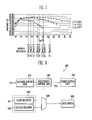
- FIG. 4 is a schematic structure diagram showing the structure of the controller of FIG. 2 ;
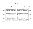
- FIG. 5 is a schematic block diagram showing the structure of the power supply unit of FIG. 2 .
- first element when a first element is described as being coupled to a second element, the first element may be not only directly coupled to the second element but may also be indirectly coupled to the second element via a third element. Further, some of the elements that are not essential to the complete understanding of the invention are omitted for clarity. Also, like reference numerals refer to like elements throughout.
- FIG. 2 is a schematic structure diagram showing an organic light emitting display device according to the present invention.
- the organic light emitting display device includes a pixel unit (or display region) 100, a data driver 200, a scan driver 300, a controller 400, a power supply unit 500, and a battery.
- the pixel unit 100 includes an organic light emitting diode on which a plurality of pixels 101 are arranged, wherein each pixel 101 light-emits light in accordance with the flow of current.
- the pixel unit 100 is arranged with n scan lines S1, S2, ... Sn-1, and Sn that transfer scan signals in a row direction and m data lines D1, D2, ... Dm-1, and Dm that transfer data signals in a column direction.
- the pixel unit 100 is driven by receiving a first power of a first power supply ELVDD and a second power of a second power supply ELVSS that has a lower level than the first power. Therefore, the pixel unit 100 is light-emitted by allowing current to be flowed onto the organic light emitting diode by the scan signals, the data signals, the first power of the first power supply ELVDD, and the second power of the second power supply ELVSS, thereby displaying an image.
- the data driver 200 receives a data driving control signal DCS and an image signal R, G, and B data from the controller 400 to generate data signals.
- the data driver 200 applies the data signals generated by being coupled to the data lines D1, D2, ... Dm-1, and Dm to the pixel unit 100.
- the data signals generated from the data driver 200 have voltage set for each gray level value, wherein the voltage set for each gray level value is determined by a gamma value.
- the gray level value is judged by the image signal R, G, and B data, and the voltage corresponding to the gray level value is determined by the gamma value so that the voltage of the data signal is determined.
- the scan driver 300 receives a scan driving control signal SCS from the controller 400 to generate scan signals.
- a scan driver 300 is coupled to the scan lines S1, S2, ... Sn-1, and Sn to transfer the scan signals to a specific row of the pixel unit 100.
- the pixel 101 transferred with (and received) the scan signal is transferred with (and received) the data signal output from the data driver 200 so that the voltage corresponding to the data signal is transferred to (and received by) the pixel 101.
- the controller 400 senses the voltage input from a battery and then controls the voltage of the data signal and the voltage of the first power supply ELVDD and the voltage of the second power supply ELVSS to correspond with the input voltage, thereby controlling the brightness of the pixel unit 100.
- the power supply unit 500 generates the first power of the first power supply ELVDD and the second power of the second power supply ELVSS by boosting or inverting the input voltage input from the external such as a battery, and transfers them to the pixel unit 100.
- the power supply unit 500 allows the voltage of the first power supply ELVDD and the voltage of the second power supply ELVSS (or the voltage between the first power supply ELVDD and the second power supply ELVSS) to correspond with the input voltage.
- FIG. 3 is a graph showing the efficiency of a power supply unit for each input voltage.
- the cases where the size of the pixel unit is 3.2 inches and 3.5 inches will be described by way of example.
- the horizontal axis of the graph represents the amount of current that flows on the entirety of the pixel unit 100 and the vertical axis of the graph represents the efficiency, thereby showing the current flowing in the cases where the input voltage is 2.9V, 3.7V, and 4.5V, and the efficiency thereof.
- the pixel unit 100 has a maximum brightness of 300cd/m 2
- current of about 120mA should be flowed in the case of the pixel unit 100 having the size of 3.2 inches and current of about 140mA should be flowed in the case of the pixel unit 100 having the size of 3.5 inches.
- the input voltage is 2.9V
- the pixel unit 100 has brightness of 200cd/m 2 or more irrespective of the size of the pixel unit 100, the efficiency thereof abruptly falls.
- the input voltage is 3.7V or more, although the pixel unit 100 maintains brightness of 300cd/m 2 , the efficiency thereof is maintained at 78% or more.
- the input voltage should maintain about 3.7V or more. Therefore, if the input voltage fails to maintain 3.7V, the power supply unit 500 stops supply of the first power of the first power supply ELVDD and the second power of the second power supply ELVSS. In other words, the pixel unit 100 cannot display an image any further.
- the pixel unit 100 has brightness of 200cd/m 2 or less, although the input voltage is about 2.9V, the efficiency is at 75% or more.
- the input voltage of 2.9V can be utilized.
- a battery outputs a high voltage after the charge thereof is completed while being used and gradually outputs a low voltage. Therefore, in order that the pixel unit 100 has brightness of 300cd/m 2 , the battery should output voltage of at least 3.7V, however, in order that the pixel unit 100 has brightness of 200cd/m 2 , the battery may output voltage of at least 2.9V. In other words, the battery has a lower voltage as time elapses so that a battery use time (or the lifespan of the battery) when the voltage of at least 2.9V is used becomes longer than a battery use time when the voltage of at least 3.7V is used.
- FIG. 4 is a schematic structure diagram showing the structure of the controller of FIG. 2 .
- the controller includes a voltage sensing unit 410, a brightness control unit 420, a selection unit 430, and a gamma storage unit 440.
- The.voltage sensing unit 410 senses the input voltage Vin output from the battery and transfers to the power supply unit 500 to allow the input voltage Vin to correspond to the voltage that is lowered according to the battery use time.
- the input voltage Vin output from the battery is frequently varied according to the load of the organic light emitting display device that receives voltage from the battery. Therefore, if the voltage sensing unit 410 measures the input voltage Vin corresponding to the change for a short time period, it will lead to a frequent brightness change so that it may have an influence on the image quality. Therefore, the input voltage Vin to be input is sampled at several time periods and then, the noise thereof is removed using a suitable median filter, etc.
- the brightness control unit 420 allows the brightness value corresponding to the input voltage Vin to be stored and allows the brightness value of the pixel unit 100 to correspond to the input voltage. In other words, if the input voltage Vin is a set (or predetermined) voltage or more, the brightness control unit 420 allows the brightness to be set to a first brightness, and if the input voltage Vin is a set (or predetermined voltage) or less, the brightness control unit 420 allows the brightness to be set to a second brightness. That is, in one embodiment, if the input voltage Vin is a first set voltage or more, the brightness control unit 420 allows the brightness to be set to the first brightness, and if the input voltage Vin is a second set voltage or less, the brightness control unit 420 allows the brightness to be set to the second brightness.
- the brightness control unit 420 if the input voltage Vin is not less than a set voltage, the brightness control unit 420 allows the brightness to be set to the first brightness, and if the input voltage Vin is less than the set voltage, the brightness control unit 420 allows the brightness to be set to the second brightness. In yet another embodiment, if the input voltage Vin is greater than a set voltage, the brightness control unit 420 allows the brightness to be set to the first brightness, and if the input voltage Vin is not greater than the set voltage, the brightness control unit 420 allows the brightness to be set to the second brightness.
- the voltage control signal VCS corresponding thereto is transferred to the selection unit 430 and the power supply unit 550.
- the brightness control unit 420 sets the set (or predetermined) values that are set to the first brightness and the second brightness to be different when the input voltage Vin is lowered from a high voltage operation to a low voltage operation and when the input voltage is raised from the low voltage operation to the high voltage operation.
- the brightness control unit 420 sets the set (or predetermined) values that are set to the first brightness and the second brightness to be different when the input voltage Vin is lowered from a high voltage operation to a low voltage operation and when the input voltage is raised from the low voltage operation to the high voltage operation.
- the brightness control unit 420 prevents the brightness from being too sensitively controlled.
- the selection unit 430 allows any one of a first gamma value or a second gamma value stored in the gamma storage unit 440 corresponding to the voltage control signal VCS transferred from the brightness control unit 420 to be transferred to the data driver 200.
- the gamma storage unit 440 includes a first register 441 in which the first gamma value is stored and a second register 442 in which the second gamma value is stored. Also, the gamma values stored in the first register 441 and the second register 442 are transferred to the data driver 200 by the selection unit 430. In addition, if the first gamma is selected, the data driver 200 outputs the data signal having a maximum brightness of about 300cd/m 2 , and if the second gamma value is selected, the data driver 200 outputs the data signal having a maximum brightness of about 200cd/m 2 .
- FIG. 5 is a schematic block diagram showing the structure of the power supply unit of FIG. 2 .
- the power supply unit 500 includes a first power generation unit that generates the first power of the first power supply ELVDD and a second power generation unit that generates the second power of the second power supply ELVSS. Also, the power supply unit 500 is operated corresponding to the voltage control signal VCS generated from the brightness control unit 420.
- the first power generation unit 501 includes a first voltage distributor 510, a first comparator 520, and a first power control block 530.
- the first voltage distributor 510 distributes the voltage of the voltage control signal VCS output from the brightness control unit 420.
- the first comparator 520 compares the voltage distributed by the first voltage distributor 510 with a reference voltage (e.g., a first reference voltage) to determine whether the first gamma value or the second gamma value is selected.
- the first power control block 530 outputs the voltage of the first power supply ELVDD from which the brightness suitable for the first gamma value or the second gamma value can be output.
- the second power generation unit 502 includes a second voltage distributor 511, a second comparator 521, and a second power control block 531.
- the second power distributor 511 distributes the voltage of the voltage control signal VCS output from the brightness control unit 420.
- the second comparator 521 compares the voltage distributed by the second voltage distributor 511 with a reference voltage (e.g., a second reference voltage) to determine whether the first gamma value or the second gamma value is selected.
- the second power control block 531 outputs the voltage of the second power supply ELVSS from which the brightness suitable for the first gamma value or the second gamma value can be output.
Landscapes
- Engineering & Computer Science (AREA)
- Physics & Mathematics (AREA)
- Computer Hardware Design (AREA)
- General Physics & Mathematics (AREA)
- Theoretical Computer Science (AREA)
- Control Of El Displays (AREA)
- Electroluminescent Light Sources (AREA)
- Control Of Indicators Other Than Cathode Ray Tubes (AREA)
Applications Claiming Priority (1)
| Application Number | Priority Date | Filing Date | Title |
|---|---|---|---|
| KR20090026475A KR101056231B1 (ko) | 2009-03-27 | 2009-03-27 | 유기전계발광표시장치 |
Publications (2)
| Publication Number | Publication Date |
|---|---|
| EP2234094A1 true EP2234094A1 (de) | 2010-09-29 |
| EP2234094B1 EP2234094B1 (de) | 2019-02-13 |
Family
ID=42229175
Family Applications (1)
| Application Number | Title | Priority Date | Filing Date |
|---|---|---|---|
| EP10250592.2A Active EP2234094B1 (de) | 2009-03-27 | 2010-03-26 | Organische lichtemittierende Anzeigevorrichtung und zugehöriges Ansteuerungsverfahren |
Country Status (5)
| Country | Link |
|---|---|
| US (1) | US9129559B2 (de) |
| EP (1) | EP2234094B1 (de) |
| JP (1) | JP2010231185A (de) |
| KR (1) | KR101056231B1 (de) |
| CN (1) | CN101847364A (de) |
Cited By (2)
| Publication number | Priority date | Publication date | Assignee | Title |
|---|---|---|---|---|
| CN103268753A (zh) * | 2013-05-28 | 2013-08-28 | 上海中科高等研究院 | 扫描线共用的amoled驱动电路及其驱动方法 |
| EP3168834A1 (de) * | 2015-11-11 | 2017-05-17 | Samsung Display Co., Ltd. | Organische lichtemittierende anzeigevorrichtung und ansteuerungsvorrichtung dafür |
Families Citing this family (8)
| Publication number | Priority date | Publication date | Assignee | Title |
|---|---|---|---|---|
| KR102139693B1 (ko) * | 2013-11-18 | 2020-07-31 | 삼성디스플레이 주식회사 | 휘도 제어 방법, 휘도 제어 유닛 및 이를 구비하는 유기 발광 표시 장치 |
| CN104464678A (zh) * | 2014-12-31 | 2015-03-25 | 深圳市华星光电技术有限公司 | 液晶显示装置及其驱动方法 |
| TWI651707B (zh) * | 2015-07-27 | 2019-02-21 | 天鈺科技股份有限公司 | 數據驅動模組及具有數據驅動模組之液晶顯示裝置 |
| CN105761692B (zh) * | 2016-05-04 | 2018-08-14 | 深圳市华星光电技术有限公司 | 用于在线调整液晶面板的伽马编码的系统 |
| CN111357045B (zh) | 2017-11-16 | 2022-03-29 | 辛纳普蒂克斯公司 | 用于显示面板的多伽玛控制技术 |
| KR101973501B1 (ko) * | 2018-06-15 | 2019-04-29 | 엘지디스플레이 주식회사 | 발광다이오드 구동회로 및 그 구동 방법 |
| KR102817921B1 (ko) * | 2019-12-30 | 2025-06-09 | 삼성디스플레이 주식회사 | 표시 장치 및 표시 장치의 구동 방법 |
| KR102668816B1 (ko) | 2020-12-22 | 2024-05-22 | 엘지디스플레이 주식회사 | 표시 장치 및 이의 저휘도 전원 제공 방법 |
Citations (2)
| Publication number | Priority date | Publication date | Assignee | Title |
|---|---|---|---|---|
| US4795972A (en) * | 1986-04-08 | 1989-01-03 | Brown, Boveri & Cie A.G. | Digital measuring method and apparatus for a quasi-analog measured value display |
| US20070146253A1 (en) * | 2005-12-22 | 2007-06-28 | Au Optronics Corporation | Method and device for brightness stabilization in AMOLED display |
Family Cites Families (17)
| Publication number | Priority date | Publication date | Assignee | Title |
|---|---|---|---|---|
| JP4083952B2 (ja) * | 1999-04-06 | 2008-04-30 | 富士フイルム株式会社 | 液晶表示装置のバックライト制御装置および方法 |
| US7119786B2 (en) * | 2001-06-28 | 2006-10-10 | Intel Corporation | Method and apparatus for enabling power management of a flat panel display |
| KR100967191B1 (ko) * | 2002-06-18 | 2010-07-05 | 캠브리지 디스플레이 테크놀로지 리미티드 | 디스플레이 드라이버 회로 |
| JP2004023939A (ja) * | 2002-06-19 | 2004-01-22 | Denso Corp | 車載用表示機器制御装置 |
| JP4826698B2 (ja) | 2004-01-21 | 2011-11-30 | セイコーエプソン株式会社 | 電気光学装置、その駆動回路及び駆動方法、並びに電子機器 |
| JP2005308857A (ja) | 2004-04-19 | 2005-11-04 | Sony Corp | アクティブマトリクス型表示装置およびその駆動方法 |
| KR20070040999A (ko) * | 2005-10-13 | 2007-04-18 | 삼성전자주식회사 | 자동 감마 및 휘도 보정 기능을 갖는 액정 표시 장치 |
| CN100359551C (zh) * | 2005-11-02 | 2008-01-02 | 友达光电股份有限公司 | 显示装置及电源装置 |
| JP4858041B2 (ja) * | 2006-09-25 | 2012-01-18 | ソニー株式会社 | 画像表示装置及びその駆動方法 |
| KR100850206B1 (ko) | 2006-12-26 | 2008-08-04 | 삼성전자주식회사 | 액정 표시 장치 및 그 화질 개선 방법 |
| KR20080090879A (ko) | 2007-04-06 | 2008-10-09 | 삼성에스디아이 주식회사 | 유기 전계 발광 표시 장치 및 그 구동 방법 |
| KR100860718B1 (ko) | 2007-04-12 | 2008-09-29 | 주식회사엘디티 | 그레이 스케일 전압을 구동 전원 전압 변동에 연동시켜서휘도 감마를 보정하는 oled 구동 장치 |
| KR100914118B1 (ko) * | 2007-04-24 | 2009-08-27 | 삼성모바일디스플레이주식회사 | 유기 전계 발광 표시 장치 및 그 구동 방법 |
| JP2008286561A (ja) * | 2007-05-15 | 2008-11-27 | Toyota Industries Corp | ノイズ除去回路とそのノイズ除去方法 |
| JP2009003243A (ja) * | 2007-06-22 | 2009-01-08 | Seiko Epson Corp | 基準電圧選択回路、表示ドライバ、電気光学装置及び電子機器 |
| KR100894606B1 (ko) * | 2007-10-29 | 2009-04-24 | 삼성모바일디스플레이주식회사 | 유기 전계 발광 표시 장치 및 그의 전원 공급 방법 |
| TWI405158B (zh) * | 2008-12-26 | 2013-08-11 | Novatek Microelectronics Corp | 可提高影像亮度並減少畫面失真之驅動方法及相關顯示裝置 |
-
2009
- 2009-03-27 KR KR20090026475A patent/KR101056231B1/ko active Active
- 2009-12-21 JP JP2009289680A patent/JP2010231185A/ja active Pending
-
2010
- 2010-01-13 US US12/686,854 patent/US9129559B2/en active Active
- 2010-03-26 EP EP10250592.2A patent/EP2234094B1/de active Active
- 2010-03-26 CN CN201010143218A patent/CN101847364A/zh active Pending
Patent Citations (2)
| Publication number | Priority date | Publication date | Assignee | Title |
|---|---|---|---|---|
| US4795972A (en) * | 1986-04-08 | 1989-01-03 | Brown, Boveri & Cie A.G. | Digital measuring method and apparatus for a quasi-analog measured value display |
| US20070146253A1 (en) * | 2005-12-22 | 2007-06-28 | Au Optronics Corporation | Method and device for brightness stabilization in AMOLED display |
Non-Patent Citations (2)
| Title |
|---|
| ANONYMOUS: "Median filter", 17 February 2009 (2009-02-17), XP002590507, Retrieved from the Internet <URL:http://en.wikipedia.org/w/index.php?title=Median_filter&oldid=277792060> [retrieved on 20100701] * |
| ANONYMOUS: "Power Manager", 18 November 2008 (2008-11-18), XP002590171, Retrieved from the Internet <URL:http://www.xphonesoftware.com/pm.html> [retrieved on 20100701] * |
Cited By (4)
| Publication number | Priority date | Publication date | Assignee | Title |
|---|---|---|---|---|
| CN103268753A (zh) * | 2013-05-28 | 2013-08-28 | 上海中科高等研究院 | 扫描线共用的amoled驱动电路及其驱动方法 |
| EP3168834A1 (de) * | 2015-11-11 | 2017-05-17 | Samsung Display Co., Ltd. | Organische lichtemittierende anzeigevorrichtung und ansteuerungsvorrichtung dafür |
| KR20170055584A (ko) * | 2015-11-11 | 2017-05-22 | 삼성디스플레이 주식회사 | 유기전계발광 표시장치 및 그의 구동방법 |
| US10290258B2 (en) | 2015-11-11 | 2019-05-14 | Samsung Display Co., Ltd. | Organic light emitting display device having adjustable power source corresponding to dimming levels and driving method thereof |
Also Published As
| Publication number | Publication date |
|---|---|
| CN101847364A (zh) | 2010-09-29 |
| EP2234094B1 (de) | 2019-02-13 |
| US9129559B2 (en) | 2015-09-08 |
| KR20100108038A (ko) | 2010-10-06 |
| KR101056231B1 (ko) | 2011-08-11 |
| US20100245319A1 (en) | 2010-09-30 |
| JP2010231185A (ja) | 2010-10-14 |
Similar Documents
| Publication | Publication Date | Title |
|---|---|---|
| EP2234094B1 (de) | Organische lichtemittierende Anzeigevorrichtung und zugehöriges Ansteuerungsverfahren | |
| US9240138B2 (en) | Organic light emitting diode display device and method for driving the same | |
| US8766971B2 (en) | Driver IC and organic light emitting display device using the same | |
| US8269703B2 (en) | Organic light emitting display device | |
| KR101142702B1 (ko) | 유기전계발광표시장치 및 그의 구동방법 | |
| US8269702B2 (en) | Organic light emitting display device and method of driving the same | |
| KR101279117B1 (ko) | 유기발광다이오드 표시소자 및 그의 구동 방법 | |
| US8638279B2 (en) | Pixel and organic light emitting display device using the same | |
| KR101760090B1 (ko) | 화소 및 이를 이용한 유기전계발광 표시장치 | |
| US20160314747A1 (en) | Organic light-emitting display device | |
| EP2439725A2 (de) | Verfahren und Vorrichtung zur Bereitstellung von Strom für eine Anzeigevorrichtung | |
| KR20120012598A (ko) | 화소 및 이를 이용한 유기전계발광 표시장치 | |
| KR101481672B1 (ko) | 유기발광다이오드 표시장치 | |
| KR101040798B1 (ko) | Dc―dc 컨버터 및 이를 이용한 유기전계발광표시장치 | |
| KR101101097B1 (ko) | 유기전계발광 표시장치 및 그의 구동방법 | |
| KR101056248B1 (ko) | 드라이버 ic 및 그를 이용한 유기전계발광표시장치 | |
| EP1895495B1 (de) | Organische elektrolumineszente Anzeigevorrichtung und Ansteuerverfahren dafür | |
| KR101022085B1 (ko) | 전원공급부 및 그를 이용한 유기전계발광표시장치 | |
| US20120062623A1 (en) | Organic light emitting display and method of driving the same | |
| KR20140077551A (ko) | 유기 전계 발광 표시 장치 및 이의 구동 방법 |
Legal Events
| Date | Code | Title | Description |
|---|---|---|---|
| PUAI | Public reference made under article 153(3) epc to a published international application that has entered the european phase |
Free format text: ORIGINAL CODE: 0009012 |
|
| 17P | Request for examination filed |
Effective date: 20100331 |
|
| AK | Designated contracting states |
Kind code of ref document: A1 Designated state(s): AT BE BG CH CY CZ DE DK EE ES FI FR GB GR HR HU IE IS IT LI LT LU LV MC MK MT NL NO PL PT RO SE SI SK SM TR |
|
| AX | Request for extension of the european patent |
Extension state: AL BA ME RS |
|
| RAP1 | Party data changed (applicant data changed or rights of an application transferred) |
Owner name: SAMSUNG DISPLAY CO., LTD. |
|
| 17Q | First examination report despatched |
Effective date: 20131120 |
|
| RAP1 | Party data changed (applicant data changed or rights of an application transferred) |
Owner name: SAMSUNG DISPLAY CO., LTD. |
|
| STAA | Information on the status of an ep patent application or granted ep patent |
Free format text: STATUS: EXAMINATION IS IN PROGRESS |
|
| GRAP | Despatch of communication of intention to grant a patent |
Free format text: ORIGINAL CODE: EPIDOSNIGR1 |
|
| STAA | Information on the status of an ep patent application or granted ep patent |
Free format text: STATUS: GRANT OF PATENT IS INTENDED |
|
| INTG | Intention to grant announced |
Effective date: 20180816 |
|
| GRAS | Grant fee paid |
Free format text: ORIGINAL CODE: EPIDOSNIGR3 |
|
| GRAA | (expected) grant |
Free format text: ORIGINAL CODE: 0009210 |
|
| STAA | Information on the status of an ep patent application or granted ep patent |
Free format text: STATUS: THE PATENT HAS BEEN GRANTED |
|
| AK | Designated contracting states |
Kind code of ref document: B1 Designated state(s): AT BE BG CH CY CZ DE DK EE ES FI FR GB GR HR HU IE IS IT LI LT LU LV MC MK MT NL NO PL PT RO SE SI SK SM TR |
|
| REG | Reference to a national code |
Ref country code: GB Ref legal event code: FG4D |
|
| REG | Reference to a national code |
Ref country code: CH Ref legal event code: EP Ref country code: AT Ref legal event code: REF Ref document number: 1096656 Country of ref document: AT Kind code of ref document: T Effective date: 20190215 |
|
| REG | Reference to a national code |
Ref country code: IE Ref legal event code: FG4D |
|
| REG | Reference to a national code |
Ref country code: DE Ref legal event code: R096 Ref document number: 602010056946 Country of ref document: DE |
|
| REG | Reference to a national code |
Ref country code: LT Ref legal event code: MG4D |
|
| REG | Reference to a national code |
Ref country code: NL Ref legal event code: MP Effective date: 20190213 |
|
| PG25 | Lapsed in a contracting state [announced via postgrant information from national office to epo] |
Ref country code: NL Free format text: LAPSE BECAUSE OF FAILURE TO SUBMIT A TRANSLATION OF THE DESCRIPTION OR TO PAY THE FEE WITHIN THE PRESCRIBED TIME-LIMIT Effective date: 20190213 Ref country code: LT Free format text: LAPSE BECAUSE OF FAILURE TO SUBMIT A TRANSLATION OF THE DESCRIPTION OR TO PAY THE FEE WITHIN THE PRESCRIBED TIME-LIMIT Effective date: 20190213 Ref country code: PT Free format text: LAPSE BECAUSE OF FAILURE TO SUBMIT A TRANSLATION OF THE DESCRIPTION OR TO PAY THE FEE WITHIN THE PRESCRIBED TIME-LIMIT Effective date: 20190613 Ref country code: FI Free format text: LAPSE BECAUSE OF FAILURE TO SUBMIT A TRANSLATION OF THE DESCRIPTION OR TO PAY THE FEE WITHIN THE PRESCRIBED TIME-LIMIT Effective date: 20190213 Ref country code: SE Free format text: LAPSE BECAUSE OF FAILURE TO SUBMIT A TRANSLATION OF THE DESCRIPTION OR TO PAY THE FEE WITHIN THE PRESCRIBED TIME-LIMIT Effective date: 20190213 Ref country code: NO Free format text: LAPSE BECAUSE OF FAILURE TO SUBMIT A TRANSLATION OF THE DESCRIPTION OR TO PAY THE FEE WITHIN THE PRESCRIBED TIME-LIMIT Effective date: 20190513 |
|
| PG25 | Lapsed in a contracting state [announced via postgrant information from national office to epo] |
Ref country code: HR Free format text: LAPSE BECAUSE OF FAILURE TO SUBMIT A TRANSLATION OF THE DESCRIPTION OR TO PAY THE FEE WITHIN THE PRESCRIBED TIME-LIMIT Effective date: 20190213 Ref country code: BG Free format text: LAPSE BECAUSE OF FAILURE TO SUBMIT A TRANSLATION OF THE DESCRIPTION OR TO PAY THE FEE WITHIN THE PRESCRIBED TIME-LIMIT Effective date: 20190513 Ref country code: GR Free format text: LAPSE BECAUSE OF FAILURE TO SUBMIT A TRANSLATION OF THE DESCRIPTION OR TO PAY THE FEE WITHIN THE PRESCRIBED TIME-LIMIT Effective date: 20190514 Ref country code: IS Free format text: LAPSE BECAUSE OF FAILURE TO SUBMIT A TRANSLATION OF THE DESCRIPTION OR TO PAY THE FEE WITHIN THE PRESCRIBED TIME-LIMIT Effective date: 20190613 Ref country code: LV Free format text: LAPSE BECAUSE OF FAILURE TO SUBMIT A TRANSLATION OF THE DESCRIPTION OR TO PAY THE FEE WITHIN THE PRESCRIBED TIME-LIMIT Effective date: 20190213 |
|
| REG | Reference to a national code |
Ref country code: AT Ref legal event code: MK05 Ref document number: 1096656 Country of ref document: AT Kind code of ref document: T Effective date: 20190213 |
|
| PG25 | Lapsed in a contracting state [announced via postgrant information from national office to epo] |
Ref country code: IT Free format text: LAPSE BECAUSE OF FAILURE TO SUBMIT A TRANSLATION OF THE DESCRIPTION OR TO PAY THE FEE WITHIN THE PRESCRIBED TIME-LIMIT Effective date: 20190213 Ref country code: DK Free format text: LAPSE BECAUSE OF FAILURE TO SUBMIT A TRANSLATION OF THE DESCRIPTION OR TO PAY THE FEE WITHIN THE PRESCRIBED TIME-LIMIT Effective date: 20190213 Ref country code: EE Free format text: LAPSE BECAUSE OF FAILURE TO SUBMIT A TRANSLATION OF THE DESCRIPTION OR TO PAY THE FEE WITHIN THE PRESCRIBED TIME-LIMIT Effective date: 20190213 Ref country code: SK Free format text: LAPSE BECAUSE OF FAILURE TO SUBMIT A TRANSLATION OF THE DESCRIPTION OR TO PAY THE FEE WITHIN THE PRESCRIBED TIME-LIMIT Effective date: 20190213 Ref country code: RO Free format text: LAPSE BECAUSE OF FAILURE TO SUBMIT A TRANSLATION OF THE DESCRIPTION OR TO PAY THE FEE WITHIN THE PRESCRIBED TIME-LIMIT Effective date: 20190213 Ref country code: CZ Free format text: LAPSE BECAUSE OF FAILURE TO SUBMIT A TRANSLATION OF THE DESCRIPTION OR TO PAY THE FEE WITHIN THE PRESCRIBED TIME-LIMIT Effective date: 20190213 Ref country code: ES Free format text: LAPSE BECAUSE OF FAILURE TO SUBMIT A TRANSLATION OF THE DESCRIPTION OR TO PAY THE FEE WITHIN THE PRESCRIBED TIME-LIMIT Effective date: 20190213 |
|
| REG | Reference to a national code |
Ref country code: CH Ref legal event code: PL |
|
| REG | Reference to a national code |
Ref country code: DE Ref legal event code: R097 Ref document number: 602010056946 Country of ref document: DE |
|
| PG25 | Lapsed in a contracting state [announced via postgrant information from national office to epo] |
Ref country code: SM Free format text: LAPSE BECAUSE OF FAILURE TO SUBMIT A TRANSLATION OF THE DESCRIPTION OR TO PAY THE FEE WITHIN THE PRESCRIBED TIME-LIMIT Effective date: 20190213 Ref country code: PL Free format text: LAPSE BECAUSE OF FAILURE TO SUBMIT A TRANSLATION OF THE DESCRIPTION OR TO PAY THE FEE WITHIN THE PRESCRIBED TIME-LIMIT Effective date: 20190213 Ref country code: LU Free format text: LAPSE BECAUSE OF NON-PAYMENT OF DUE FEES Effective date: 20190326 |
|
| REG | Reference to a national code |
Ref country code: BE Ref legal event code: MM Effective date: 20190331 |
|
| PLBE | No opposition filed within time limit |
Free format text: ORIGINAL CODE: 0009261 |
|
| STAA | Information on the status of an ep patent application or granted ep patent |
Free format text: STATUS: NO OPPOSITION FILED WITHIN TIME LIMIT |
|
| PG25 | Lapsed in a contracting state [announced via postgrant information from national office to epo] |
Ref country code: AT Free format text: LAPSE BECAUSE OF FAILURE TO SUBMIT A TRANSLATION OF THE DESCRIPTION OR TO PAY THE FEE WITHIN THE PRESCRIBED TIME-LIMIT Effective date: 20190213 Ref country code: MC Free format text: LAPSE BECAUSE OF FAILURE TO SUBMIT A TRANSLATION OF THE DESCRIPTION OR TO PAY THE FEE WITHIN THE PRESCRIBED TIME-LIMIT Effective date: 20190213 |
|
| 26N | No opposition filed |
Effective date: 20191114 |
|
| PG25 | Lapsed in a contracting state [announced via postgrant information from national office to epo] |
Ref country code: IE Free format text: LAPSE BECAUSE OF NON-PAYMENT OF DUE FEES Effective date: 20190326 Ref country code: CH Free format text: LAPSE BECAUSE OF NON-PAYMENT OF DUE FEES Effective date: 20190331 Ref country code: LI Free format text: LAPSE BECAUSE OF NON-PAYMENT OF DUE FEES Effective date: 20190331 |
|
| PG25 | Lapsed in a contracting state [announced via postgrant information from national office to epo] |
Ref country code: BE Free format text: LAPSE BECAUSE OF NON-PAYMENT OF DUE FEES Effective date: 20190331 Ref country code: SI Free format text: LAPSE BECAUSE OF FAILURE TO SUBMIT A TRANSLATION OF THE DESCRIPTION OR TO PAY THE FEE WITHIN THE PRESCRIBED TIME-LIMIT Effective date: 20190213 |
|
| PG25 | Lapsed in a contracting state [announced via postgrant information from national office to epo] |
Ref country code: TR Free format text: LAPSE BECAUSE OF FAILURE TO SUBMIT A TRANSLATION OF THE DESCRIPTION OR TO PAY THE FEE WITHIN THE PRESCRIBED TIME-LIMIT Effective date: 20190213 |
|
| PG25 | Lapsed in a contracting state [announced via postgrant information from national office to epo] |
Ref country code: MT Free format text: LAPSE BECAUSE OF NON-PAYMENT OF DUE FEES Effective date: 20190326 |
|
| PG25 | Lapsed in a contracting state [announced via postgrant information from national office to epo] |
Ref country code: CY Free format text: LAPSE BECAUSE OF FAILURE TO SUBMIT A TRANSLATION OF THE DESCRIPTION OR TO PAY THE FEE WITHIN THE PRESCRIBED TIME-LIMIT Effective date: 20190213 |
|
| PG25 | Lapsed in a contracting state [announced via postgrant information from national office to epo] |
Ref country code: HU Free format text: LAPSE BECAUSE OF FAILURE TO SUBMIT A TRANSLATION OF THE DESCRIPTION OR TO PAY THE FEE WITHIN THE PRESCRIBED TIME-LIMIT; INVALID AB INITIO Effective date: 20100326 |
|
| PG25 | Lapsed in a contracting state [announced via postgrant information from national office to epo] |
Ref country code: MK Free format text: LAPSE BECAUSE OF FAILURE TO SUBMIT A TRANSLATION OF THE DESCRIPTION OR TO PAY THE FEE WITHIN THE PRESCRIBED TIME-LIMIT Effective date: 20190213 |
|
| P01 | Opt-out of the competence of the unified patent court (upc) registered |
Effective date: 20230515 |
|
| PGFP | Annual fee paid to national office [announced via postgrant information from national office to epo] |
Ref country code: GB Payment date: 20260224 Year of fee payment: 17 |
|
| PGFP | Annual fee paid to national office [announced via postgrant information from national office to epo] |
Ref country code: DE Payment date: 20260220 Year of fee payment: 17 |
|
| PGFP | Annual fee paid to national office [announced via postgrant information from national office to epo] |
Ref country code: FR Payment date: 20260224 Year of fee payment: 17 |