EP2237565A2 - Dispositif et procédé d'affichage - Google Patents
Dispositif et procédé d'affichage Download PDFInfo
- Publication number
- EP2237565A2 EP2237565A2 EP20100157512 EP10157512A EP2237565A2 EP 2237565 A2 EP2237565 A2 EP 2237565A2 EP 20100157512 EP20100157512 EP 20100157512 EP 10157512 A EP10157512 A EP 10157512A EP 2237565 A2 EP2237565 A2 EP 2237565A2
- Authority
- EP
- European Patent Office
- Prior art keywords
- image
- display
- luminance
- drive compensation
- signal
- Prior art date
- Legal status (The legal status is an assumption and is not a legal conclusion. Google has not performed a legal analysis and makes no representation as to the accuracy of the status listed.)
- Granted
Links
Images







Classifications
-
- H—ELECTRICITY
- H04—ELECTRIC COMMUNICATION TECHNIQUE
- H04N—PICTORIAL COMMUNICATION, e.g. TELEVISION
- H04N13/00—Stereoscopic video systems; Multi-view video systems; Details thereof
- H04N13/30—Image reproducers
- H04N13/398—Synchronisation thereof; Control thereof
-
- G—PHYSICS
- G09—EDUCATION; CRYPTOGRAPHY; DISPLAY; ADVERTISING; SEALS
- G09G—ARRANGEMENTS OR CIRCUITS FOR CONTROL OF INDICATING DEVICES USING STATIC MEANS TO PRESENT VARIABLE INFORMATION
- G09G3/00—Control arrangements or circuits, of interest only in connection with visual indicators other than cathode-ray tubes
- G09G3/001—Control arrangements or circuits, of interest only in connection with visual indicators other than cathode-ray tubes using specific devices not provided for in groups G09G3/02 - G09G3/36, e.g. using an intermediate record carrier such as a film slide; Projection systems; Display of non-alphanumerical information, solely or in combination with alphanumerical information, e.g. digital display on projected diapositive as background
- G09G3/003—Control arrangements or circuits, of interest only in connection with visual indicators other than cathode-ray tubes using specific devices not provided for in groups G09G3/02 - G09G3/36, e.g. using an intermediate record carrier such as a film slide; Projection systems; Display of non-alphanumerical information, solely or in combination with alphanumerical information, e.g. digital display on projected diapositive as background to produce spatial visual effects
-
- G—PHYSICS
- G09—EDUCATION; CRYPTOGRAPHY; DISPLAY; ADVERTISING; SEALS
- G09G—ARRANGEMENTS OR CIRCUITS FOR CONTROL OF INDICATING DEVICES USING STATIC MEANS TO PRESENT VARIABLE INFORMATION
- G09G3/00—Control arrangements or circuits, of interest only in connection with visual indicators other than cathode-ray tubes
- G09G3/20—Control arrangements or circuits, of interest only in connection with visual indicators other than cathode-ray tubes for presentation of an assembly of a number of characters, e.g. a page, by composing the assembly by combination of individual elements arranged in a matrix no fixed position being assigned to or needed to be assigned to the individual characters or partial characters
- G09G3/34—Control arrangements or circuits, of interest only in connection with visual indicators other than cathode-ray tubes for presentation of an assembly of a number of characters, e.g. a page, by composing the assembly by combination of individual elements arranged in a matrix no fixed position being assigned to or needed to be assigned to the individual characters or partial characters by control of light from an independent source
- G09G3/36—Control arrangements or circuits, of interest only in connection with visual indicators other than cathode-ray tubes for presentation of an assembly of a number of characters, e.g. a page, by composing the assembly by combination of individual elements arranged in a matrix no fixed position being assigned to or needed to be assigned to the individual characters or partial characters by control of light from an independent source using liquid crystals
- G09G3/3611—Control of matrices with row and column drivers
-
- H—ELECTRICITY
- H04—ELECTRIC COMMUNICATION TECHNIQUE
- H04N—PICTORIAL COMMUNICATION, e.g. TELEVISION
- H04N13/00—Stereoscopic video systems; Multi-view video systems; Details thereof
- H04N13/30—Image reproducers
- H04N13/332—Displays for viewing with the aid of special glasses or head-mounted displays [HMD]
- H04N13/341—Displays for viewing with the aid of special glasses or head-mounted displays [HMD] using temporal multiplexing
-
- G—PHYSICS
- G09—EDUCATION; CRYPTOGRAPHY; DISPLAY; ADVERTISING; SEALS
- G09G—ARRANGEMENTS OR CIRCUITS FOR CONTROL OF INDICATING DEVICES USING STATIC MEANS TO PRESENT VARIABLE INFORMATION
- G09G2320/00—Control of display operating conditions
- G09G2320/02—Improving the quality of display appearance
- G09G2320/0285—Improving the quality of display appearance using tables for spatial correction of display data
-
- G—PHYSICS
- G09—EDUCATION; CRYPTOGRAPHY; DISPLAY; ADVERTISING; SEALS
- G09G—ARRANGEMENTS OR CIRCUITS FOR CONTROL OF INDICATING DEVICES USING STATIC MEANS TO PRESENT VARIABLE INFORMATION
- G09G2340/00—Aspects of display data processing
- G09G2340/16—Determination of a pixel data signal depending on the signal applied in the previous frame
Definitions
- the present invention relates to a display device and a display method.
- Display devices exist in which an image displayed on a screen is perceived by a viewer as a stereoscopic image.
- a time sharing display system is known as a technique to cause the viewer to perceive an image displayed on this type of display device as a stereoscopic image.
- the time sharing display system alternately displays an image for the left eye and an image for the right eye on the entire screen at very short intervals (refer to Japanese Patent Application Publication No. JP-A-9-138384 , Japanese Patent Application Publication No. JP-A-2000-36969 and Japanese Patent Application Publication No. JP-A-2003-45343 ).
- An image displayed by the time sharing display system can be perceived by the viewer as a stereoscopic image through shutter glasses worn by the viewer.
- a left eye shutter a liquid crystal shutter, for example
- a right eye shutter of the shutter glasses is closed to shut off the light from the screen.
- the left eye shutter of the shutter glasses is closed to shut off the light from the screen, and the right eye shutter of the shutter glasses is opened to allow the light from the screen to pass through.
- crosstalk may occur due to characteristics of the display device and the shutter glasses, such as an insufficient liquid crystal response speed (when a liquid crystal panel is used as a screen) and insufficient contrast of the liquid crystal shutters of the shutter glasses.
- Crosstalk is a phenomenon in which a part of the image for the right eye enters into the left eye and a part of the image for the left eye enters into the right eye.
- a method to improve crosstalk a method has been proposed in which the display panel is driven at a high speed (for example, 240 Hz), and an image for the left eye and an image for the right eye are each displayed on the screen two times repeatedly.
- the shutter glasses are opened only in a period during which each of the images is displayed for the second time.
- image writing is performed in a line sequential manner, from the upper edge to the lower edge of the screen.
- the screen has a position in which crosstalk worsens.
- a display device including a display portion that line-sequentially displays, in an image display region, a first image based on a first image signal and a second image based on a second image signal, by sequentially switching the first image and the second image at a predetermined interval and a drive compensation portion that performs predetermined drive compensation on the first image signal and the second image signal input to the display portion, in accordance with a position of the image display region, a luminance of the first image and a luminance of the second image, such that an average luminance of one of the first image and the second image becomes substantially uniform in the image display region during a predetermined period that is shorter than the predetermined interval.
- the display portion line-sequentially displays, in the image display region, the first image based on the first image signal and the second image based on the second image signal, by sequentially switching the first image and the second image at the predetermined interval.
- the drive compensation portion performs the predetermined drive compensation on the first image signal and the second image signal input to the display portion, in accordance with the position of the image display region, the luminance of the first image and the luminance of the second image, such that the average luminance of the first image or the second image becomes substantially uniform in the image display region during a predetermined period that is shorter than the predetermined interval.
- the drive compensation portion may include a drive compensation parameter storage portion that stores parameters used in the predetermined drive compensation, and a drive compensation execution portion that performs drive compensation on the first image signal and the second image signal, in accordance with the parameters stored in the drive compensation parameter storage portion.
- the drive compensation portion may perform the predetermined drive compensation in a period other than the predetermined period.
- the parameters stored in the drive compensation parameter storage portion may have values that are different from each other with respect to a writing direction of the first image signal and the second image signal to the image display region.
- the drive compensation parameter storage portion may have parameters that are different from each other in accordance with a plurality of regions in the image display region.
- the drive compensation execution portion may perform drive compensation using parameters that continuously vary in accordance with the position of the image display region.
- the drive compensation execution portion may generate the parameters that continuously vary in accordance with the position of the image display region, by interpolating parameters that are given in accordance with the position of the image display region.
- the display portion may be a liquid crystal panel.
- the predetermined period may be a period during which light from the display portion is allowed to enter the eyes of a viewer.
- a display method including the steps of acquiring a first image signal and a second image signal that are input to a display portion that displays a first image based on the first image signal and a second image based on the second image signal on an image display region by sequentially switching the first image and the second image at a predetermined interval, acquiring a position of the image display region, a luminance of the first image and a luminance of the second image, performing predetermined drive compensation on the first image signal and the second image signal acquired in the signal acquiring step, in accordance with the position and the luminances acquired in the acquiring step, such that an average luminance of one of the first image and the second image becomes substantially uniform in the image display region during a predetermined period that is shorter than the predetermined interval, and displaying, in the image display region, the first image based on the first image signal and the second image based on the second image signal by sequentially switching the first image and the second image at the predetermined interval, the first image signal and the second image
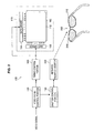
- FIG. 1 is an explanatory diagram showing the outer appearance of the display device 100 according to the embodiment of the present invention. Additionally, FIG. 1 also shows shutter glasses 200, which are used to cause a viewer to perceive an image displayed on the display device 100 as a stereoscopic image.
- the display device 100 shown in FIG. 1 is provided with an image display portion 110 that displays images.
- the display device 100 does not only display normal images on the image display portion 110, but can also display three-dimensional images on the image display portion 110 that are perceived by the viewer as stereoscopic images.
- the image display portion 110 includes a light source, a liquid crystal panel and a pair of polarizing plates that sandwich the liquid crystal panel. Light from the light source is polarized in a predetermined direction by passing through the liquid crystal panel and the polarizing plates.
- the shutter glasses 200 include a right eye image transmission portion 212 and a left eye image transmission portion 214, which are liquid crystal shutters, for example.
- the shutter glasses 200 perform opening and closing operations of the right eye image transmission portion 212 and the left eye image transmission portion 214, in response to a signal transmitted from the display device 100.
- the viewer can perceive an image displayed on the image display portion 110 as a stereoscopic image, by looking at the light emitted from the image display portion 110 through the right eye image transmission portion 212 and the left eye image transmission portion 214 of the shutter glasses 200.
- the display device 100 is portrayed as a television receiver, but the present invention is naturally not limited to this example of the form of the display device 100.
- the display device 100 according to the present invention may be, for example, a monitor that is used when connected to an electronic appliance such as a personal computer or the like, or it may be a mobile game console, a mobile telephone, or a portable music playback device and so on.
- the outer appearance of the display device 100 according to the embodiment of the present invention is described above. Next, the functional structure of the display device 100 according to the embodiment of the present invention will be explained.
- FIG. 2 is an explanatory diagram showing the functional structure of the display device 100 according to the embodiment of the present invention.
- the functional structure of the display device 100 according to the embodiment of the present invention will be explained with reference to FIG. 2 .
- the display device 100 includes the image display portion 110, a video signal control portion 120, a shutter control portion 130, a timing control portion 140 and an infrared radiation emitter 150.
- the image display portion 110 displays images in the manner described above, and when a signal is applied from an external source, display of images is performed in accordance with the applied signal.
- the image display portion 110 includes a display panel 112, a gate driver 113, a data driver 114 and a backlight 115.
- the display panel 112 displays images in accordance with the signal applied from an external source.
- the display panel 112 displays images by sequentially scanning a plurality of scanning lines.
- Liquid crystal molecules having a predetermined orientation are filled in a space between transparent plates, made of glass or the like, of the display panel 112.
- a drive system of the display panel 112 may be a twisted nematic (TN) system, a vertical alignment (VA) system, or an in-place-switching (IPS) system.
- TN twisted nematic
- VA vertical alignment
- IPS in-place-switching
- the display panel 112 is a display panel that can rewrite the screen at a high-speed frame rate (240 Hz, for example).
- a high-speed frame rate 240 Hz, for example.
- an image for the right eye and an image for the left eye are displayed alternately on the display panel 112 at a predetermined timing, thereby causing the viewer to perceive a stereoscopic image.
- the gate driver 113 is a driver that drives a gate bus line (not shown in the figures) of the display panel 112. A signal is transmitted from the timing control portion 140 to the gate driver 113, and the gate driver 113 outputs a signal to the gate bus line in accordance with the signal transmitted from the timing control portion 140.
- the data driver 114 is a driver that generates a signal that is applied to a data line (not shown in the figures) of the display panel 112. A signal is transmitted from the timing control portion 140 to the data driver 114. The data driver 114 generates a signal to be applied to the data line, in accordance with the signal transmitted from the timing control portion 140, and outputs the generated signal.
- the backlight 115 is provided on the furthermost side of the image display portion 110 as seen from the side of the viewer.
- white light that is not polarized (unpolarized light) is output from the backlight 115 to the display panel 112 positioned on the side of the viewer.
- the backlight 115 may use a light-emitting diode, for example, or may use a cold cathode tube.
- the backlight 115 shown in FIG. 2 is a surface light source, but the present invention is not limited to this form of light source.
- the light source may be arranged around the peripheral edges of the display panel 112, and may output light to the display panel 112 by diffusing the light from the light source using a diffuser panel etc.
- a point light source and a condenser lens may be used in combination in place of the surface light source.
- the video signal control portion 120 When the video signal control portion 120 receives a video signal from an external source, the video signal control portion 120 performs various types of signal processing on the received video signal such that it is suitable for three-dimensional image display on the image display portion 110 and outputs the processed signal.
- the video signal on which signal processing has been performed by the video signal control portion 120 is transmitted to the timing control portion 140. Further, when the video signal control portion 120 performs signal processing, it transmits a predetermined signal to the shutter control portion 130 in accordance with the signal processing.
- the signal processing by the video signal control portion 120 is, for example, as described below.
- the video signal control portion 120 When a video signal to display the image for the right eye on the image display portion 110 (a right eye video signal) and a video signal to display the image for the left eye on the image display portion 110 (a left eye video signal) are received by the video signal control portion 120, the video signal control portion 120 generates, from the two received video signals, a video signal for a three-dimensional image.
- the video signal control portion 120 generates, from the received right eye video signal and the left eye video signal, video signals to display images on the display panel 112 in the following order: image for the right eye ⁇ image for the right eye ⁇ image for the left eye ⁇ mage for the left eye ⁇ image for the right eye ⁇ image for the right eye ⁇ and so on.
- the shutter control portion 130 receives the predetermined signal that is generated in accordance with the signal processing by the video signal control portion 120, and generates a shutter control signal that controls shutter operation of the shutter glasses 200 in accordance with the predetermined signal.
- the shutter glasses 200 perform opening and closing operations of the right eye image transmission portion 212 and the left eye image transmission portion 214, based on the shutter control signal that is generated by the shutter control portion 130 and output from the infrared radiation emitter 150.
- the timing control portion 140 In accordance with the signal transmitted from the video signal control portion 120, the timing control portion 140 generates a pulse signal that is used to operate the gate driver 113 and the data driver 114.
- the pulse signal is generated by the timing control portion 140, and the gate driver 113 and the data driver 114 receive the pulse signal generated by the timing control portion 140, an image corresponding to the signal transmitted from the video signal control portion 120 is displayed on the display panel 112.
- the timing control portion 140 performs predetermined signal processing when it generates the pulse signal used to operate the gate driver 113 and the data driver 114.
- the timing control portion 140 is an example of a drive compensation portion of the present invention.
- the predetermined signal processing in the timing control portion 140 makes it possible to improve crosstalk in a period during which the shutters of the shutter glasses 200 are opened.
- the predetermined signal processing in the timing control portion 140 will be described in detail later.
- the functional structure of the display device 100 according to the embodiment of the present invention is explained above. Next, the structure of the timing control portion 140 according to the embodiment of the present invention will be explained.
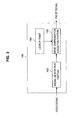
- FIG. 3 is an explanatory diagram showing the structure of the timing control portion 140 according to the embodiment of the present invention.
- the structure of the timing control portion 140 according to the embodiment of the present invention will be explained with reference to FIG. 3 .
- the timing control portion 140 includes a signal generation portion 162, a lookup table 164 and a drive compensation execution portion 166.
- the signal generation portion 162 generates a pulse signal used to operate the gate driver 113 and the data driver 114, in accordance with a signal transmitted from the video signal control portion 120.
- the signal generation portion 162 generates the pulse signal, and the gate driver 113 and the data driver 114 operate based on the pulse signal. As a result, an image is displayed on the display panel 112.
- the pulse signal generated by the signal generation portion 162 is transmitted to the drive compensation execution portion 166.
- the lookup table 164 is an example of a drive compensation parameter storage portion of the present invention, and is a table that stores parameters to be used for signal processing in the drive compensation execution portion 166. Note that, in the present embodiment, the drive compensation execution portion 166 performs overdrive processing as signal processing in the drive compensation execution portion 166.
- the parameters stored in the lookup table 164 may be parameters that vary depending on regions of the display panel 112.
- the lookup table 164 may store parameters that correspond to a plurality of positions in a scanning direction (a direction in which the image signal generated by the signal generation portion 162 is written) of the display panel 112.
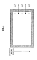
- FIG. 4 is an explanatory diagram showing the parameters that are stored in the lookup table 164 and that correspond to the plurality of positions in the scanning direction of the display panel 112.
- FIG. 4 shows that different parameters LUT1 to LUT5, which are used for overdrive processing in the drive compensation execution portion 166, are stored in the lookup table 164, from the upper section to the lower section of the display panel 112.
- the parameters LUT1 to LUT5 stored in the lookup table 164 may be parameters whose values vary continuously.
- the relationship between the parameters and their positions in the display panel 112 is not limited to this example.
- a plurality of different parameters that correspond to the direction from the left to the right of the display panel 112 (or the direction opposite to that direction) may be stored in the lookup table 164.
- the parameter of the certain region may be determined by interpolation processing with respect to that parameter, using parameters corresponding to the upper and lower regions of the certain region.
- the number of the parameters may be appropriately set in accordance with a write speed of the image signal to the display panel 112, and a response speed of the liquid crystal molecules with which the display panel 112 is filled.
- the drive compensation execution portion 166 performs signal processing on the pulse signal generated by the signal generation portion 162. As described above, in the present embodiment, the drive compensation execution portion 166 performs overdrive processing, as signal processing in the drive compensation execution portion 166. The drive compensation execution portion 166 performs signal processing on the pulse signal used to operate the gate driver 113 and the data driver 144, thereby compensating pixel drive on the display panel 112.
- timing control portion 140 The structure of the timing control portion 140 according to the embodiment of the present invention is explained above. Next, the operation of the display device 100 according to the embodiment of the present invention will be explained. Before explaining the operation of the display device 100 according to the embodiment of the present invention, a crosstalk improvement method used in a known display device that displays three dimensional images and problems thereof will be explained.
- FIG. 5 is an explanatory diagram showing, in a time series, liquid crystal response of a display panel, backlight response and shutter glasses response, in the known display device that displays three dimensional images.
- the display panel is sequentially scanned from the uppermost section. Therefore, a time difference in the liquid crystal response occurs between the uppermost section and the lowermost section of the display panel.
- a display time per frame is approximately 4.2 milliseconds.
- the interval to display them is approximately 16.7 milliseconds. In this case, the backlight is kept on.
- a shutter open period of the shutter glasses at this time is approximately 2.1 milliseconds, which corresponds to 12.5 percent of the interval when the image for the right eye and the image for the left eye are each displayed two times continuously, for example.
- the image for the right eye and the image for the left eye are each displayed two times continuously, and the shutter glasses are opened only for a part of the second display.
- This enables a three dimensional display in which the image for the right eye and the image for the left eye are not mixed together. Further, the same image is displayed two times continuously. Therefore, as compared to a case where the images are simply alternately displayed once each, it is possible to achieve a desired luminance on both the upper side and the lower side of the display panel.
- FIG. 6 is an explanatory diagram showing an example of luminance response waveforms in the known display device that displays three dimensional images.
- FIG. 6 shows luminance response waveforms in the upper section of the screen, the central section of the screen and the lower section of the screen, using the same time axis.
- the image for the right eye and the image for the left eye are each displayed two times continuously by the known display device, and if the shutter glasses are opened only for a part of the second display, image display with a desired luminance is performed for all the shutter open period in the central section of the screen when the image is seen through the shutter glasses.
- image display is performed at a luminance that deviates from the desired luminance.
- the term "desired luminance” represents a luminance at which, when an image displayed in all image display regions of the display panel is viewed through the shutter glasses, the image can be viewed without crosstalk.
- overdrive parameters that vary depending on the position on the screen are prepared, as will be described below. Then, the prepared overdrive parameters that vary depending on the position on the screen are used to compensate drive of the display panel so that a desired luminance is achieved in any section of the screen. If overdrive parameters that vary in this manner are prepared and the drive of the display panel is compensated, it is possible to reduce crosstalk.
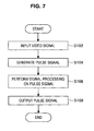
- FIG. 7 is a flowchart illustrating the drive compensation method in the display device 100 according to the embodiment of the present invention.
- the drive compensation method in the display device 100 according to the embodiment of the present invention will be explained with reference to FIG. 7 .
- a video signal transmitted from the video signal control portion 120 is input to the timing control portion 140 (step S102).
- the signal generation portion 162 generates, from the input video signal, a pulse signal used to operate the gate driver 113 and the data driver 114 (step S104).
- the generated pulse signal is transmitted to the drive compensation execution portion 166.
- the drive compensation execution portion 166 When the signal generation portion 162 generates the pulse signal used to operate the gate driver 113 and the data driver 114 and transmits the generated pulse signal to the drive compensation execution portion 166, the drive compensation execution portion 166 performs signal processing on the received pulse signal (step S106).
- the signal processing on the pulse signal performed by the drive compensation execution portion 166 is overdrive processing to obtain a desired luminance during an open period of the shutter glasses 200.
- the drive compensation execution portion 166 performs the overdrive processing using the overdrive parameters stored in the lookup table 164.
- the overdrive parameters may be parameters that vary depending on the position on the display panel 112 as shown in FIG. 4 .
- the drive compensation execution portion 166 When the drive compensation execution portion 166 performs signal processing on the pulse signal, the drive compensation execution portion 166 then outputs the processed pulse signal (step S108).
- the pulse signal output from the drive compensation execution portion 166 is input to the gate driver 113 and the data driver 114.
- the gate driver 113 and the data driver 114 supply a signal to the display panel 112 based on the pulse signal output from the drive compensation execution portion 166.
- the display panel 112 displays an image based on the signal on which signal processing has been performed by the drive compensation execution portion 166.
- the viewer looks at the image display on the display panel 112 through the shutter glasses 200, the viewer can see the image displayed at a desired luminance, regardless of the position on the screen. Thus, it is possible to improve crosstalk.
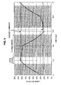
- FIG. 8 is an explanatory diagram showing, in the form of a graph, an improvement example of intermediate gradation in the upper section of the screen of the display panel 112, when the overdrive processing by the drive compensation execution portion 166 is performed.
- FIG. 8 shows luminance response when an image for the right eye and an image for the left eye are displayed on the display panel 112 two times continuously.
- the first display (of the image for the left eye, for example) is performed on the display panel 112 in a period from 0 to 4.2 msec
- the second display is performed on the display panel 112 in a period from 4.2 to 8.4 msec.
- the first display (of the image for the right eye, for example) is performed on the display panel 112 in a period from 8.4 to 12.6 msec, and the second display is performed on the display panel 112 in a period from 12.6 to 16.8 msec. In this manner, the display of the image for the right eye and the display of the image for the left eye are sequentially repeated.
- the shutters of the shutter glasses 200 are opened in the shutter open period. More specifically, in a period during which the second display of the image for the right eye (or the image for the left eye) is performed on the display panel 112, and in a period during which the first display of the image for the left eye (or the image for the right eye) is performed on the display panel 112, the left eye image transmission portion 214 (or the right eye image transmission portion 212) of the shutter glasses 200 is opened. In a time period other than the shutter open period is a time period during which the shutters of the shutter glasses 200 are closed (a shutter closed period).
- the waveform shown by the dotted line indicates a change in luminance ratio when the known overdrive processing that optimizes the central section of the screen is performed.
- the waveform shown by the solid line indicates a change in luminance ratio when the overdrive processing by the drive compensation execution portion 166 is performed.
- the vertical axis represents luminance ratios with respect to the most brightly displayed state, which is taken as 100 percent.
- the shutter open period and the shutter closed period of the shutter glasses 200 are shown by changes in the background of the graph.
- the desired luminance during the shutter open period of the shutter glasses 200 is shown at two locations on a high luminance side and a low luminance side.
- the luminance starts to decrease or increase from the desired luminance when half of the shutter open period of the shutter glasses 200 has elapsed. Therefore, when the overdrive processing is not performed, display with a desired luminance is not performed for all the shutter open period of the shutter glasses 200.
- the luminance may be increased or decreased, not only during the shutter open period of the shutter glasses 200 as shown in FIG. 8 , but also during the shutter closed period of the shutter glasses 200.
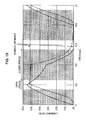
- FIG. 9 is an explanatory diagram showing, in the form of a graph, an improvement example of intermediate gradation in the lower section of the screen of the display panel 112, when the overdrive processing by the drive compensation execution portion 166 is performed.
- the waveform shown by the dotted line indicates a change in luminance ratio when the known overdrive processing that optimizes the central section of the screen is performed.
- the waveform shown by the solid line indicates a change in luminance ratio when the overdrive processing by the drive compensation execution portion 166 is performed.
- FIG. 9 similar to FIG. 8 , the waveform shown by the dotted line indicates a change in luminance ratio when the known overdrive processing that optimizes the central section of the screen is performed.
- the waveform shown by the solid line indicates a change in luminance ratio when the overdrive processing by the drive compensation execution portion 166 is performed.
- FIG. 9 similar to FIG. 8 , the waveform shown by the dotted line indicates a change in luminance ratio when the known overdrive processing that optimizes the central section of the screen is performed
- the first display (of the image for the left eye, for example) is performed on the display panel 112 in a period from 0 to 4.2 msec, and the second display is performed on the display panel 112 in a period from 4.2 to 8.4 msec. Further, the first display (of the image for the right eye, for example) is performed on the display panel 112 in a period from 8.4 to 12.6 msec, and the second display is performed on the display panel 112 in a period from 12.6 to 16.8 msec. In this manner, the display of the image for the right eye and the display of the image for the left eye are sequentially repeated. Note that, although the shutter open periods are different in FIG. 8 and FIG. 9 , this is for ease of explanation. The shutter open periods in the upper section and the lower section of the screen of the display panel 112 are the same.
- the desired luminance is at last reached when half of the shutter open period of the shutter glasses 200 has elapsed. Therefore, when the overdrive processing is not performed, display with a desired luminance is not performed for all the shutter open period of the shutter glasses 200.
- the luminance may be increased or decreased, not only during the shutter open period of the shutter glasses 200 as shown in FIG. 9 , but also during the shutter closed period of the shutter glasses 200.
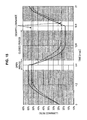
- FIG. 10 is an explanatory diagram showing, in the form of a graph, an improvement example of high gradation in the upper section of the screen of the display panel 112, when the overdrive processing by the drive compensation execution portion 166 is performed.
- the waveform shown by the dotted line indicates a change in luminance ratio when the known overdrive processing that optimizes the central section of the screen is performed.
- the waveform shown by the solid line indicates a change in luminance ratio when the overdrive processing by the drive compensation execution portion 166 is performed.
- the shutter open period and the shutter closed period exist at the same timings as in the example shown in FIG. 8 .
- the luminance starts to decrease or increase from the desired luminance when half of the shutter open period of the shutter glasses 200 has elapsed. Therefore, when the overdrive processing is not performed, display with a desired luminance is not performed for all the shutter open period of the shutter glasses 200.
- the desired luminance can be approached by performing the overdrive processing by the drive compensation execution portion 166.
- high gradation display it may not be possible to increase the luminance during the shutter open period of the shutter glasses 200.
- the luminance ratio of the desired luminance is 100 percent, more improvement in luminance cannot be expected. Therefore, in the present embodiment, when high gradation display is performed, the luminance is improved during the shutter closed period of the shutter glasses 200. More specifically, overdrive processing that increases a voltage value of the next frame is performed. By performing the overdrive processing that improves the luminance during the shutter closed period of the shutter glasses 200, it is possible to suppress a decrease in luminance during the shutter open period of the shutter glasses 200. Further, with this overdrive processing, the average luminance can be caused to coincide with or approach the desired luminance for all the shutter open period of the shutter glasses 200.
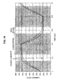
- FIG. 11 is an explanatory diagram showing, in the form of a graph, an improvement example of high gradation in the lower section of the screen of the display panel 112, when the overdrive processing by the drive compensation execution portion 166 is performed.
- the waveform shown by the dotted line indicates a change in luminance ratio when the known overdrive processing that optimizes the central section of the screen is performed.
- the waveform shown by the solid line indicates a change in luminance ratio when the overdrive processing by the drive compensation execution portion 166 is performed.
- the shutter open period and the shutter closed period exist at the same timings as in the example shown in FIG. 9 .
- the shutter open periods are different in FIG. 10 and FIG. 11 , this is for ease of explanation.
- the shutter open periods in the upper section and the lower section of the screen of the display panel 112 are the same.
- the desired luminance is at last reached when the shutter open period of the shutter glasses 200 ends. Therefore, when the overdrive processing is not performed, display with a desired luminance is not performed for all the shutter open period of the shutter glasses 200.
- the desired luminance can be approached by performing the overdrive processing by the drive compensation execution portion 166.
- the luminance is improved during the shutter closed period of the shutter glasses 200. More specifically, overdrive processing that increases a voltage value of the previous frame is performed.
- FIG. 12 is an explanatory diagram showing, in the form of a graph, an improvement example of low gradation in the upper section of the screen of the display panel 112, when the overdrive processing by the drive compensation execution portion 166 is performed.
- the waveform shown by the dotted line indicates a change in luminance ratio when the known overdrive processing that optimizes the central section of the screen is performed.
- the waveform shown by the solid line indicates a change in luminance ratio when the overdrive processing by the drive compensation execution portion 166 is performed. Note that, in the example shown in FIG. 12 , the shutter open period and the shutter closed period exist at the same timings as in the example shown in FIG. 8 .
- the luminance starts to increase or decrease from the desired luminance when half of the shutter open period of the shutter glasses 200 has elapsed. Therefore, when the overdrive processing is not performed, display with a desired luminance is not performed for all the shutter open period of the shutter glasses 200.
- the luminance is decreased during the shutter closed period of the shutter glasses 200. More specifically, by performing overdrive processing that reduces a voltage value of the next frame, the average luminance can be caused to coincide with or approach the desired luminance during the shutter open period of the shutter glasses 200 in which display is performed on the high luminance side and the low luminance side.
- FIG. 13 is an explanatory diagram showing, in the form of a graph, an improvement example of low gradation in the lower section of the screen of the display panel 112, when the overdrive processing by the drive compensation execution portion 166 is performed.
- the waveform shown by the dotted line indicates a change in luminance ratio when the known overdrive processing that optimizes the central section of the screen is performed.
- the waveform shown by the solid line indicates a change in luminance ratio when the overdrive processing by the drive compensation execution portion 166 is performed.
- the shutter open period and the shutter closed period exist at the same timings as in the example shown in FIG. 9 . Although the shutter open periods are different in FIG. 12 and FIG. 13 , this is for ease of explanation.
- the shutter open periods in the upper section and the lower section of the screen of the display panel 112 are the same.
- the desired luminance is reached when half of the shutter open period of the shutter glasses 200 has elapsed, or the desired luminance is at last reached when the shutter open period ends. Therefore, when the overdrive processing is not performed, display with a desired luminance is not performed for all the shutter open period of the shutter glasses 200.
- the luminance is increased during the shutter closed period of the shutter glasses 200. More specifically, by performing overdrive processing that reduces a voltage value of the previous frame, the average luminance can be caused to coincide with or approach the desired luminance, during the shutter open period of the shutter glasses 200 in which display is performed on the high luminance side and the low luminance side.
- drive compensation during the shutter open period of the shutter glasses 200 may be applied to cases other than the case where the image for the right eye and the image for the left eye are displayed two or more times continuously as shown in FIG. 5 . More specifically, the drive compensation during the shutter open period of the shutter glasses 200 may also be performed in a case where the image for the right eye and the image for the left eye are alternately displayed once each.
- FIG. 14 is an explanatory diagram showing, in the form of a graph, an example of change in luminance in the central section of the screen, when an image for the right eye and an image for the left eye are alternately displayed once each.
- display with a desired luminance is performed for all the shutter open period of the shutter glasses 200.
- display with a desired luminance is not performed for all the shutter open period of the shutter glasses 200 in the upper section and the lower section of the screen.
- FIG. 15 is an explanatory diagram showing, in the form of a graph, an improvement example in the upper section of the screen of the display panel 112, when the overdrive processing by the drive compensation execution portion 166 is performed in a case where an image for the right eye and an image for the left eye are alternately displayed once each.
- the waveform shown by the dotted line indicates a change in luminance ratio when the known overdrive processing that optimizes the central section of the screen is performed.
- the waveform shown by the solid line indicates a change in luminance ratio when the overdrive processing by the drive compensation execution portion 166 is performed. Note that, in the example shown in FIG. 15 , the shutter open period and the shutter closed period exist at the same timings as in the example shown in FIG. 8 .
- the luminance starts to decrease or increase from the desired luminance when half of the shutter open period of the shutter glasses 200 has elapsed. Therefore, when the overdrive processing is not performed, display with a desired luminance is not performed for all the shutter open period of the shutter glasses 200.
- the average luminance can be caused to coincide with or approach the desired luminance, during the shutter open period of the shutter glasses 200 in which display is performed on the high luminance side and the low luminance side.
- FIG. 16 is an explanatory diagram showing, in the form of a graph, an improvement example in the lower section of the screen of the display panel 112, when the overdrive processing by the drive compensation execution portion 166 is performed in a case where an image for the right eye and an image for the left eye are alternately displayed once each.
- the waveform shown by the dotted line indicates a change in luminance ratio when the known overdrive processing that optimizes the central section of the screen is performed.
- the waveform shown by the solid line indicates a change in luminance ratio when the overdrive processing by the drive compensation execution portion 166 is performed. Note that, in the example shown in FIG.
- the shutter open period and the shutter closed period exist at the same timings as in the example shown in FIG. 9 .
- the shutter open periods are different in FIG. 15 and FIG. 16 , this is for ease of explanation.
- the shutter open periods in the upper section and the lower section of the screen of the display panel 112 are the same.
- the desired luminance is at last reached when the shutter open period of the shutter glasses 200 has elapsed. Therefore, when the overdrive processing is not performed, display with a desired luminance is not performed for all the shutter open period of the shutter glasses 200.
- the average luminance can be caused to coincide with or approach the desired luminance, during the shutter open period of the shutter glasses 200 in which display is performed on the high luminance side and the low luminance side.
- the drive compensation execution portion 166 performs drive compensation during the shutter open period of the shutter glasses 200 such that the average value of the luminance of an image displayed on the display panel 112 is caused to coincide with or approach a desired luminance.
- the drive compensation performed by the drive compensation execution portion 166 is over drive processing that increases or decreases the luminance during the shutter open period or the shutter closed period of the shutter glasses 200, for example.
- the drive compensation is performed by the drive compensation execution portion 166, the average value of the luminance of the displayed image during the shutter open period of the shutter glasses 200 can be caused to coincide with or approach the desired luminance in all the regions of the display panel 112.
- drive compensation processing in the above-described timing control portion 140 may be performed by hardware or software.
- a storage medium that stores a program for example, may be incorporated in the display device 100.
- the program may be read and executed sequentially by a central processing unit (CPU), a digital signal processor (DSP) or another control device incorporated in the display device 100.
- CPU central processing unit
- DSP digital signal processor
- the overdrive processing is performed after a pulse signal is generated.
- the pulse signal may be generated after the overdrive processing is performed, and the generated pulse signal may be supplied to the display panel.
- the present application contains subject matter related to that disclosed in Japanese Priority Patent Application JP 2009-86376 filed in the Japan Patent Office on 31 March, 2009.
Landscapes
- Engineering & Computer Science (AREA)
- General Physics & Mathematics (AREA)
- Theoretical Computer Science (AREA)
- Physics & Mathematics (AREA)
- Computer Hardware Design (AREA)
- Multimedia (AREA)
- Signal Processing (AREA)
- Chemical & Material Sciences (AREA)
- Crystallography & Structural Chemistry (AREA)
- Control Of Indicators Other Than Cathode Ray Tubes (AREA)
- Liquid Crystal Display Device Control (AREA)
- Liquid Crystal (AREA)
- Testing, Inspecting, Measuring Of Stereoscopic Televisions And Televisions (AREA)
Applications Claiming Priority (1)
| Application Number | Priority Date | Filing Date | Title |
|---|---|---|---|
| JP2009086376A JP5702054B2 (ja) | 2009-03-31 | 2009-03-31 | 表示装置及び表示方法 |
Publications (3)
| Publication Number | Publication Date |
|---|---|
| EP2237565A2 true EP2237565A2 (de) | 2010-10-06 |
| EP2237565A3 EP2237565A3 (de) | 2013-08-21 |
| EP2237565B1 EP2237565B1 (de) | 2016-09-07 |
Family
ID=42184132
Family Applications (1)
| Application Number | Title | Priority Date | Filing Date |
|---|---|---|---|
| EP10157512.4A Not-in-force EP2237565B1 (de) | 2009-03-31 | 2010-03-24 | Anzeigevorrichtung und Anzeigeverfahren |
Country Status (4)
| Country | Link |
|---|---|
| US (1) | US9066094B2 (de) |
| EP (1) | EP2237565B1 (de) |
| JP (1) | JP5702054B2 (de) |
| CN (1) | CN101854561B (de) |
Families Citing this family (21)
| Publication number | Priority date | Publication date | Assignee | Title |
|---|---|---|---|---|
| KR101698570B1 (ko) * | 2010-03-25 | 2017-01-23 | 삼성디스플레이 주식회사 | 표시 장치 및 그 구동 방법 |
| KR101281989B1 (ko) * | 2010-04-21 | 2013-07-03 | 엘지디스플레이 주식회사 | 액정 표시장치의 구동장치 및 구동방법 |
| KR101753801B1 (ko) * | 2010-06-10 | 2017-07-04 | 엘지디스플레이 주식회사 | 액정 표시장치 및 구동방법 |
| KR101279128B1 (ko) * | 2010-07-08 | 2013-06-26 | 엘지디스플레이 주식회사 | 입체 영상 표시장치와 그 구동 방법 |
| TWI424395B (zh) * | 2010-07-21 | 2014-01-21 | Chunghwa Picture Tubes Ltd | 立體顯示器 |
| KR20120019728A (ko) * | 2010-08-26 | 2012-03-07 | 엘지전자 주식회사 | 영상표시장치 및 그 동작방법 |
| JP5261533B2 (ja) * | 2010-09-14 | 2013-08-14 | パナソニック株式会社 | 情報表示装置、再生装置、および立体映像表示装置 |
| KR101734458B1 (ko) * | 2010-11-05 | 2017-05-12 | 삼성디스플레이 주식회사 | 입체 영상 표시 장치 및 그의 구동 방법 |
| KR101212170B1 (ko) * | 2010-12-10 | 2012-12-13 | 엘지디스플레이 주식회사 | 패턴드 리타더를 이용한 입체 영상 표시 장치 및 그 구동 방법 |
| JP2012128197A (ja) * | 2010-12-15 | 2012-07-05 | Toshiba Corp | 立体画像表示装置および立体画像表示方法 |
| WO2012099354A2 (ko) * | 2011-01-17 | 2012-07-26 | (주)쓰리디랩스 | 영상물 재생 및 시청 방법과 시스템 |
| KR101782818B1 (ko) * | 2011-01-21 | 2017-09-29 | 삼성디스플레이 주식회사 | 데이터 처리 방법, 데이터 구동 회로 및 이를 포함하는 표시 장치 |
| CN102833556A (zh) * | 2011-06-16 | 2012-12-19 | 群康科技(深圳)有限公司 | 立体显示装置 |
| KR101873475B1 (ko) * | 2011-07-07 | 2018-07-03 | 엘지디스플레이 주식회사 | 입체영상 표시장치와 그 구동방법 |
| JP2013064920A (ja) * | 2011-09-20 | 2013-04-11 | Seiko Epson Corp | 電気光学装置および電子機器 |
| US9591346B2 (en) | 2012-05-14 | 2017-03-07 | Samsung Electronics Co., Ltd. | Content delivery system with content sharing mechanism and method of operation thereof |
| CN105208365B (zh) * | 2014-06-20 | 2018-05-15 | 青岛海信电器股份有限公司 | 一种显示信号处理方法、装置及显示设备 |
| CN105632420A (zh) * | 2016-03-16 | 2016-06-01 | 京东方科技集团股份有限公司 | 背光模组监控系统和方法以及显示装置 |
| CN107068100B (zh) * | 2017-05-19 | 2019-09-20 | 硅谷数模半导体(北京)有限公司 | 液晶面板显示画面的方法和装置 |
| US12093452B2 (en) * | 2022-01-19 | 2024-09-17 | Prilit Optronics, Inc. | Mixed reality display system |
| US20250240401A1 (en) * | 2024-01-22 | 2025-07-24 | Vision Products, Llc | Augmented reality system with fail-safe direct view mode |
Citations (4)
| Publication number | Priority date | Publication date | Assignee | Title |
|---|---|---|---|---|
| JPH09138384A (ja) | 1995-11-15 | 1997-05-27 | Sanyo Electric Co Ltd | 立体画像観察用眼鏡の制御方法 |
| JP2000036969A (ja) | 1998-07-21 | 2000-02-02 | Nippon Hoso Kyokai <Nhk> | 立体画像表示方法および装置 |
| JP2003045343A (ja) | 2001-08-03 | 2003-02-14 | Nippon Hoso Kyokai <Nhk> | 立体画像表示装置 |
| JP2009086376A (ja) | 2007-09-28 | 2009-04-23 | Fujifilm Corp | 感光性組成物、感光性フィルム、感光性積層体、永久パターン形成方法、プリント基板 |
Family Cites Families (24)
| Publication number | Priority date | Publication date | Assignee | Title |
|---|---|---|---|---|
| JPH0973049A (ja) * | 1995-06-29 | 1997-03-18 | Canon Inc | 画像表示方法及びそれを用いた画像表示装置 |
| US6532008B1 (en) * | 2000-03-13 | 2003-03-11 | Recherches Point Lab Inc. | Method and apparatus for eliminating steroscopic cross images |
| US6765568B2 (en) * | 2000-06-12 | 2004-07-20 | Vrex, Inc. | Electronic stereoscopic media delivery system |
| US7898519B2 (en) * | 2005-02-17 | 2011-03-01 | Sharp Laboratories Of America, Inc. | Method for overdriving a backlit display |
| JP4376764B2 (ja) * | 2004-12-01 | 2009-12-02 | 三菱電機株式会社 | 立体画像表示装置 |
| KR101136791B1 (ko) * | 2004-12-27 | 2012-04-19 | 엘지디스플레이 주식회사 | 입체영상표시장치용 인터페이스 회로부와 이를 이용한 3디입체영상 구동방법 |
| JP2006330171A (ja) * | 2005-05-24 | 2006-12-07 | Sharp Corp | 液晶表示装置 |
| EP1883835A4 (de) * | 2005-05-26 | 2011-04-13 | Real D | Geisterbild-kompensation für verbesserte stereo-projektion |
| US7724211B2 (en) * | 2006-03-29 | 2010-05-25 | Nvidia Corporation | System, method, and computer program product for controlling stereo glasses shutters |
| US8872754B2 (en) * | 2006-03-29 | 2014-10-28 | Nvidia Corporation | System, method, and computer program product for controlling stereo glasses shutters |
| CN1852445B (zh) * | 2006-05-15 | 2010-08-04 | 郁有华 | 平面、立体两用显示器 |
| EP1879173A1 (de) | 2006-07-11 | 2008-01-16 | Hannstar Display Corporation | Flüssigkristallanzeige und deren Übersteuerungsverfahren |
| US8085217B2 (en) * | 2006-08-08 | 2011-12-27 | Nvidia Corporation | System, method, and computer program product for compensating for crosstalk during the display of stereo content |
| US20100060723A1 (en) * | 2006-11-08 | 2010-03-11 | Nec Corporation | Display system |
| JP2008158472A (ja) * | 2006-11-29 | 2008-07-10 | Mitsubishi Electric Corp | 液晶表示装置 |
| US7898603B2 (en) * | 2006-11-30 | 2011-03-01 | Reald Inc. | Double-shutter lenses with compensators |
| US8355097B2 (en) * | 2007-06-05 | 2013-01-15 | Samsung Electronics Co., Ltd. | Liquid crystal display and control method thereof |
| JP4304637B2 (ja) * | 2007-06-06 | 2009-07-29 | ソニー株式会社 | 液晶プロジェクタおよび液晶プロジェクタの制御方法 |
| US20080316303A1 (en) * | 2007-06-08 | 2008-12-25 | Joseph Chiu | Display Device |
| JP5309488B2 (ja) * | 2007-07-18 | 2013-10-09 | セイコーエプソン株式会社 | 電気光学装置及び電子機器 |
| JP4760799B2 (ja) * | 2007-08-07 | 2011-08-31 | ソニー株式会社 | 液晶プロジェクタおよび液晶プロジェクタの制御方法 |
| JP2009292993A (ja) | 2008-06-09 | 2009-12-17 | Alcare Co Ltd | 蓄熱用ゲル体及びこれを使用した保冷・保温材 |
| US8542326B2 (en) * | 2008-11-17 | 2013-09-24 | X6D Limited | 3D shutter glasses for use with LCD displays |
| KR20100076230A (ko) * | 2008-12-26 | 2010-07-06 | 삼성전자주식회사 | 액정표시장치 및 그 표시방법 |
-
2009
- 2009-03-31 JP JP2009086376A patent/JP5702054B2/ja not_active Expired - Fee Related
-
2010
- 2010-03-23 US US12/661,737 patent/US9066094B2/en not_active Expired - Fee Related
- 2010-03-24 EP EP10157512.4A patent/EP2237565B1/de not_active Not-in-force
- 2010-03-24 CN CN201010140777XA patent/CN101854561B/zh not_active Expired - Fee Related
Patent Citations (4)
| Publication number | Priority date | Publication date | Assignee | Title |
|---|---|---|---|---|
| JPH09138384A (ja) | 1995-11-15 | 1997-05-27 | Sanyo Electric Co Ltd | 立体画像観察用眼鏡の制御方法 |
| JP2000036969A (ja) | 1998-07-21 | 2000-02-02 | Nippon Hoso Kyokai <Nhk> | 立体画像表示方法および装置 |
| JP2003045343A (ja) | 2001-08-03 | 2003-02-14 | Nippon Hoso Kyokai <Nhk> | 立体画像表示装置 |
| JP2009086376A (ja) | 2007-09-28 | 2009-04-23 | Fujifilm Corp | 感光性組成物、感光性フィルム、感光性積層体、永久パターン形成方法、プリント基板 |
Also Published As
| Publication number | Publication date |
|---|---|
| CN101854561B (zh) | 2013-07-24 |
| JP2010239474A (ja) | 2010-10-21 |
| US20100245400A1 (en) | 2010-09-30 |
| EP2237565A3 (de) | 2013-08-21 |
| EP2237565B1 (de) | 2016-09-07 |
| JP5702054B2 (ja) | 2015-04-15 |
| US9066094B2 (en) | 2015-06-23 |
| CN101854561A (zh) | 2010-10-06 |
Similar Documents
| Publication | Publication Date | Title |
|---|---|---|
| US9066094B2 (en) | Display device and display method | |
| US9077985B2 (en) | Video display device and system | |
| US8564627B2 (en) | Image display device and method of driving image display device | |
| US20110090321A1 (en) | Display device, display method and computer program | |
| EP2306743A2 (de) | Bildanzeigevorrichtung, Bildanzeigeansichtssystem und Bildanzeigeverfahren | |
| CN102238402B (zh) | 用于驱动液晶显示装置的设备和方法 | |
| US20110157260A1 (en) | 3d image display device | |
| US20110007136A1 (en) | Image signal processing apparatus and image display | |
| US8681188B2 (en) | Display device, display method and computer program | |
| JP2010210712A (ja) | 画像表示装置、画像表示観察システム及び画像表示方法 | |
| CN101923221A (zh) | 图像显示设备和使用该图像显示设备的图像显示系统 | |
| JP2011252943A (ja) | 立体表示システム | |
| US9261706B2 (en) | Display device, display method and computer program | |
| US8780175B2 (en) | Picture signal processor, picture display and picture display system | |
| JP5405660B2 (ja) | 立体映像表示方法および立体映像表示装置 | |
| US20110304709A1 (en) | Video display apparatus and video viewing system | |
| US20120127162A1 (en) | Method for displaying a stereoscopic image and display apparatus for performing the same | |
| JP2007271842A (ja) | 表示装置 | |
| US9426456B2 (en) | Display device and video viewing system | |
| KR20120035825A (ko) | 3d 디스플레이 패널 및 이를 이용하는 3d 디스플레이 장치와 그 구동 방법 | |
| CN102918860A (zh) | 液晶显示装置 | |
| JP2011075668A (ja) | 画像表示装置およびその駆動方法 | |
| JP2011040947A (ja) | 画像処理装置及びプログラム |
Legal Events
| Date | Code | Title | Description |
|---|---|---|---|
| PUAI | Public reference made under article 153(3) epc to a published international application that has entered the european phase |
Free format text: ORIGINAL CODE: 0009012 |
|
| 17P | Request for examination filed |
Effective date: 20100324 |
|
| AK | Designated contracting states |
Kind code of ref document: A2 Designated state(s): AT BE BG CH CY CZ DE DK EE ES FI FR GB GR HR HU IE IS IT LI LT LU LV MC MK MT NL NO PL PT RO SE SI SK SM TR |
|
| REG | Reference to a national code |
Ref country code: DE Ref legal event code: R079 Ref document number: 602010036136 Country of ref document: DE Free format text: PREVIOUS MAIN CLASS: H04N0013000000 Ipc: G09G0003360000 |
|
| PUAL | Search report despatched |
Free format text: ORIGINAL CODE: 0009013 |
|
| AK | Designated contracting states |
Kind code of ref document: A3 Designated state(s): AT BE BG CH CY CZ DE DK EE ES FI FR GB GR HR HU IE IS IT LI LT LU LV MC MK MT NL NO PL PT RO SE SI SK SM TR |
|
| RIC1 | Information provided on ipc code assigned before grant |
Ipc: G09G 3/36 20060101AFI20130716BHEP |
|
| 17Q | First examination report despatched |
Effective date: 20140523 |
|
| GRAP | Despatch of communication of intention to grant a patent |
Free format text: ORIGINAL CODE: EPIDOSNIGR1 |
|
| INTG | Intention to grant announced |
Effective date: 20160405 |
|
| GRAS | Grant fee paid |
Free format text: ORIGINAL CODE: EPIDOSNIGR3 |
|
| GRAA | (expected) grant |
Free format text: ORIGINAL CODE: 0009210 |
|
| AK | Designated contracting states |
Kind code of ref document: B1 Designated state(s): AT BE BG CH CY CZ DE DK EE ES FI FR GB GR HR HU IE IS IT LI LT LU LV MC MK MT NL NO PL PT RO SE SI SK SM TR |
|
| REG | Reference to a national code |
Ref country code: GB Ref legal event code: FG4D |
|
| REG | Reference to a national code |
Ref country code: CH Ref legal event code: EP |
|
| REG | Reference to a national code |
Ref country code: IE Ref legal event code: FG4D |
|
| REG | Reference to a national code |
Ref country code: DE Ref legal event code: R096 Ref document number: 602010036136 Country of ref document: DE |
|
| REG | Reference to a national code |
Ref country code: AT Ref legal event code: REF Ref document number: 827480 Country of ref document: AT Kind code of ref document: T Effective date: 20161015 |
|
| REG | Reference to a national code |
Ref country code: LT Ref legal event code: MG4D |
|
| REG | Reference to a national code |
Ref country code: NL Ref legal event code: MP Effective date: 20160907 |
|
| PG25 | Lapsed in a contracting state [announced via postgrant information from national office to epo] |
Ref country code: LT Free format text: LAPSE BECAUSE OF FAILURE TO SUBMIT A TRANSLATION OF THE DESCRIPTION OR TO PAY THE FEE WITHIN THE PRESCRIBED TIME-LIMIT Effective date: 20160907 Ref country code: NO Free format text: LAPSE BECAUSE OF FAILURE TO SUBMIT A TRANSLATION OF THE DESCRIPTION OR TO PAY THE FEE WITHIN THE PRESCRIBED TIME-LIMIT Effective date: 20161207 Ref country code: FI Free format text: LAPSE BECAUSE OF FAILURE TO SUBMIT A TRANSLATION OF THE DESCRIPTION OR TO PAY THE FEE WITHIN THE PRESCRIBED TIME-LIMIT Effective date: 20160907 Ref country code: HR Free format text: LAPSE BECAUSE OF FAILURE TO SUBMIT A TRANSLATION OF THE DESCRIPTION OR TO PAY THE FEE WITHIN THE PRESCRIBED TIME-LIMIT Effective date: 20160907 |
|
| REG | Reference to a national code |
Ref country code: FR Ref legal event code: PLFP Year of fee payment: 8 |
|
| REG | Reference to a national code |
Ref country code: AT Ref legal event code: MK05 Ref document number: 827480 Country of ref document: AT Kind code of ref document: T Effective date: 20160907 |
|
| PG25 | Lapsed in a contracting state [announced via postgrant information from national office to epo] |
Ref country code: LV Free format text: LAPSE BECAUSE OF FAILURE TO SUBMIT A TRANSLATION OF THE DESCRIPTION OR TO PAY THE FEE WITHIN THE PRESCRIBED TIME-LIMIT Effective date: 20160907 Ref country code: ES Free format text: LAPSE BECAUSE OF FAILURE TO SUBMIT A TRANSLATION OF THE DESCRIPTION OR TO PAY THE FEE WITHIN THE PRESCRIBED TIME-LIMIT Effective date: 20160907 Ref country code: GR Free format text: LAPSE BECAUSE OF FAILURE TO SUBMIT A TRANSLATION OF THE DESCRIPTION OR TO PAY THE FEE WITHIN THE PRESCRIBED TIME-LIMIT Effective date: 20161208 Ref country code: SE Free format text: LAPSE BECAUSE OF FAILURE TO SUBMIT A TRANSLATION OF THE DESCRIPTION OR TO PAY THE FEE WITHIN THE PRESCRIBED TIME-LIMIT Effective date: 20160907 Ref country code: NL Free format text: LAPSE BECAUSE OF FAILURE TO SUBMIT A TRANSLATION OF THE DESCRIPTION OR TO PAY THE FEE WITHIN THE PRESCRIBED TIME-LIMIT Effective date: 20160907 |
|
| PG25 | Lapsed in a contracting state [announced via postgrant information from national office to epo] |
Ref country code: RO Free format text: LAPSE BECAUSE OF FAILURE TO SUBMIT A TRANSLATION OF THE DESCRIPTION OR TO PAY THE FEE WITHIN THE PRESCRIBED TIME-LIMIT Effective date: 20160907 Ref country code: EE Free format text: LAPSE BECAUSE OF FAILURE TO SUBMIT A TRANSLATION OF THE DESCRIPTION OR TO PAY THE FEE WITHIN THE PRESCRIBED TIME-LIMIT Effective date: 20160907 |
|
| PG25 | Lapsed in a contracting state [announced via postgrant information from national office to epo] |
Ref country code: CZ Free format text: LAPSE BECAUSE OF FAILURE TO SUBMIT A TRANSLATION OF THE DESCRIPTION OR TO PAY THE FEE WITHIN THE PRESCRIBED TIME-LIMIT Effective date: 20160907 Ref country code: PT Free format text: LAPSE BECAUSE OF FAILURE TO SUBMIT A TRANSLATION OF THE DESCRIPTION OR TO PAY THE FEE WITHIN THE PRESCRIBED TIME-LIMIT Effective date: 20170109 Ref country code: AT Free format text: LAPSE BECAUSE OF FAILURE TO SUBMIT A TRANSLATION OF THE DESCRIPTION OR TO PAY THE FEE WITHIN THE PRESCRIBED TIME-LIMIT Effective date: 20160907 Ref country code: SK Free format text: LAPSE BECAUSE OF FAILURE TO SUBMIT A TRANSLATION OF THE DESCRIPTION OR TO PAY THE FEE WITHIN THE PRESCRIBED TIME-LIMIT Effective date: 20160907 Ref country code: BE Free format text: LAPSE BECAUSE OF FAILURE TO SUBMIT A TRANSLATION OF THE DESCRIPTION OR TO PAY THE FEE WITHIN THE PRESCRIBED TIME-LIMIT Effective date: 20160907 Ref country code: SM Free format text: LAPSE BECAUSE OF FAILURE TO SUBMIT A TRANSLATION OF THE DESCRIPTION OR TO PAY THE FEE WITHIN THE PRESCRIBED TIME-LIMIT Effective date: 20160907 Ref country code: IS Free format text: LAPSE BECAUSE OF FAILURE TO SUBMIT A TRANSLATION OF THE DESCRIPTION OR TO PAY THE FEE WITHIN THE PRESCRIBED TIME-LIMIT Effective date: 20170107 Ref country code: PL Free format text: LAPSE BECAUSE OF FAILURE TO SUBMIT A TRANSLATION OF THE DESCRIPTION OR TO PAY THE FEE WITHIN THE PRESCRIBED TIME-LIMIT Effective date: 20160907 Ref country code: BG Free format text: LAPSE BECAUSE OF FAILURE TO SUBMIT A TRANSLATION OF THE DESCRIPTION OR TO PAY THE FEE WITHIN THE PRESCRIBED TIME-LIMIT Effective date: 20161207 |
|
| REG | Reference to a national code |
Ref country code: DE Ref legal event code: R097 Ref document number: 602010036136 Country of ref document: DE |
|
| PG25 | Lapsed in a contracting state [announced via postgrant information from national office to epo] |
Ref country code: IT Free format text: LAPSE BECAUSE OF FAILURE TO SUBMIT A TRANSLATION OF THE DESCRIPTION OR TO PAY THE FEE WITHIN THE PRESCRIBED TIME-LIMIT Effective date: 20160907 |
|
| PLBE | No opposition filed within time limit |
Free format text: ORIGINAL CODE: 0009261 |
|
| STAA | Information on the status of an ep patent application or granted ep patent |
Free format text: STATUS: NO OPPOSITION FILED WITHIN TIME LIMIT |
|
| PG25 | Lapsed in a contracting state [announced via postgrant information from national office to epo] |
Ref country code: DK Free format text: LAPSE BECAUSE OF FAILURE TO SUBMIT A TRANSLATION OF THE DESCRIPTION OR TO PAY THE FEE WITHIN THE PRESCRIBED TIME-LIMIT Effective date: 20160907 |
|
| 26N | No opposition filed |
Effective date: 20170608 |
|
| PG25 | Lapsed in a contracting state [announced via postgrant information from national office to epo] |
Ref country code: SI Free format text: LAPSE BECAUSE OF FAILURE TO SUBMIT A TRANSLATION OF THE DESCRIPTION OR TO PAY THE FEE WITHIN THE PRESCRIBED TIME-LIMIT Effective date: 20160907 |
|
| REG | Reference to a national code |
Ref country code: CH Ref legal event code: PL |
|
| PG25 | Lapsed in a contracting state [announced via postgrant information from national office to epo] |
Ref country code: MC Free format text: LAPSE BECAUSE OF FAILURE TO SUBMIT A TRANSLATION OF THE DESCRIPTION OR TO PAY THE FEE WITHIN THE PRESCRIBED TIME-LIMIT Effective date: 20160907 |
|
| REG | Reference to a national code |
Ref country code: IE Ref legal event code: MM4A |
|
| PG25 | Lapsed in a contracting state [announced via postgrant information from national office to epo] |
Ref country code: LU Free format text: LAPSE BECAUSE OF NON-PAYMENT OF DUE FEES Effective date: 20170324 |
|
| REG | Reference to a national code |
Ref country code: FR Ref legal event code: PLFP Year of fee payment: 9 |
|
| PG25 | Lapsed in a contracting state [announced via postgrant information from national office to epo] |
Ref country code: LI Free format text: LAPSE BECAUSE OF NON-PAYMENT OF DUE FEES Effective date: 20170331 Ref country code: IE Free format text: LAPSE BECAUSE OF NON-PAYMENT OF DUE FEES Effective date: 20170324 Ref country code: CH Free format text: LAPSE BECAUSE OF NON-PAYMENT OF DUE FEES Effective date: 20170331 |
|
| PG25 | Lapsed in a contracting state [announced via postgrant information from national office to epo] |
Ref country code: MT Free format text: LAPSE BECAUSE OF NON-PAYMENT OF DUE FEES Effective date: 20170324 |
|
| PGFP | Annual fee paid to national office [announced via postgrant information from national office to epo] |
Ref country code: GB Payment date: 20190222 Year of fee payment: 10 Ref country code: DE Payment date: 20190219 Year of fee payment: 10 |
|
| PGFP | Annual fee paid to national office [announced via postgrant information from national office to epo] |
Ref country code: FR Payment date: 20190220 Year of fee payment: 10 |
|
| PG25 | Lapsed in a contracting state [announced via postgrant information from national office to epo] |
Ref country code: HU Free format text: LAPSE BECAUSE OF FAILURE TO SUBMIT A TRANSLATION OF THE DESCRIPTION OR TO PAY THE FEE WITHIN THE PRESCRIBED TIME-LIMIT; INVALID AB INITIO Effective date: 20100324 |
|
| PG25 | Lapsed in a contracting state [announced via postgrant information from national office to epo] |
Ref country code: CY Free format text: LAPSE BECAUSE OF NON-PAYMENT OF DUE FEES Effective date: 20160907 |
|
| PG25 | Lapsed in a contracting state [announced via postgrant information from national office to epo] |
Ref country code: MK Free format text: LAPSE BECAUSE OF FAILURE TO SUBMIT A TRANSLATION OF THE DESCRIPTION OR TO PAY THE FEE WITHIN THE PRESCRIBED TIME-LIMIT Effective date: 20160907 |
|
| PG25 | Lapsed in a contracting state [announced via postgrant information from national office to epo] |
Ref country code: TR Free format text: LAPSE BECAUSE OF FAILURE TO SUBMIT A TRANSLATION OF THE DESCRIPTION OR TO PAY THE FEE WITHIN THE PRESCRIBED TIME-LIMIT Effective date: 20160907 |
|
| REG | Reference to a national code |
Ref country code: DE Ref legal event code: R119 Ref document number: 602010036136 Country of ref document: DE |
|
| PG25 | Lapsed in a contracting state [announced via postgrant information from national office to epo] |
Ref country code: FR Free format text: LAPSE BECAUSE OF NON-PAYMENT OF DUE FEES Effective date: 20200331 Ref country code: DE Free format text: LAPSE BECAUSE OF NON-PAYMENT OF DUE FEES Effective date: 20201001 |
|
| GBPC | Gb: european patent ceased through non-payment of renewal fee |
Effective date: 20200324 |
|
| PG25 | Lapsed in a contracting state [announced via postgrant information from national office to epo] |
Ref country code: GB Free format text: LAPSE BECAUSE OF NON-PAYMENT OF DUE FEES Effective date: 20200324 |