EP2239722A2 - Procédé d'acquisition de valeur de correction, procédé de correction et appareil d'affichage d'images - Google Patents
Procédé d'acquisition de valeur de correction, procédé de correction et appareil d'affichage d'images Download PDFInfo
- Publication number
- EP2239722A2 EP2239722A2 EP10155434A EP10155434A EP2239722A2 EP 2239722 A2 EP2239722 A2 EP 2239722A2 EP 10155434 A EP10155434 A EP 10155434A EP 10155434 A EP10155434 A EP 10155434A EP 2239722 A2 EP2239722 A2 EP 2239722A2
- Authority
- EP
- European Patent Office
- Prior art keywords
- gradation level
- luminance
- correction value
- electron
- correction
- Prior art date
- Legal status (The legal status is an assumption and is not a legal conclusion. Google has not performed a legal analysis and makes no representation as to the accuracy of the status listed.)
- Withdrawn
Links
- 238000012937 correction Methods 0.000 title claims abstract description 209
- 238000000034 method Methods 0.000 title claims description 30
- 239000006185 dispersion Substances 0.000 claims abstract description 82
- 238000004364 calculation method Methods 0.000 claims description 14
- 238000005259 measurement Methods 0.000 description 20
- 238000006243 chemical reaction Methods 0.000 description 17
- 239000011159 matrix material Substances 0.000 description 16
- 238000010586 diagram Methods 0.000 description 12
- 239000000126 substance Substances 0.000 description 8
- 230000003247 decreasing effect Effects 0.000 description 6
- 230000007423 decrease Effects 0.000 description 4
- 238000013213 extrapolation Methods 0.000 description 4
- 230000006870 function Effects 0.000 description 4
- 238000004020 luminiscence type Methods 0.000 description 4
- 230000008707 rearrangement Effects 0.000 description 3
- OKTJSMMVPCPJKN-UHFFFAOYSA-N Carbon Chemical compound [C] OKTJSMMVPCPJKN-UHFFFAOYSA-N 0.000 description 2
- 239000002041 carbon nanotube Substances 0.000 description 2
- 229910021393 carbon nanotube Inorganic materials 0.000 description 2
- 238000005516 engineering process Methods 0.000 description 2
- 238000004519 manufacturing process Methods 0.000 description 2
- 239000002184 metal Substances 0.000 description 2
- 230000003287 optical effect Effects 0.000 description 2
- 238000013139 quantization Methods 0.000 description 2
- 230000001174 ascending effect Effects 0.000 description 1
- 230000008859 change Effects 0.000 description 1
- 230000006835 compression Effects 0.000 description 1
- 238000007906 compression Methods 0.000 description 1
- 238000007796 conventional method Methods 0.000 description 1
- 230000001934 delay Effects 0.000 description 1
- 230000000694 effects Effects 0.000 description 1
- 230000006872 improvement Effects 0.000 description 1
- 238000012986 modification Methods 0.000 description 1
- 230000004048 modification Effects 0.000 description 1
- 238000012545 processing Methods 0.000 description 1
- 230000035945 sensitivity Effects 0.000 description 1
- 238000004088 simulation Methods 0.000 description 1
- 239000000758 substrate Substances 0.000 description 1
Images


Classifications
-
- G—PHYSICS
- G09—EDUCATION; CRYPTOGRAPHY; DISPLAY; ADVERTISING; SEALS
- G09G—ARRANGEMENTS OR CIRCUITS FOR CONTROL OF INDICATING DEVICES USING STATIC MEANS TO PRESENT VARIABLE INFORMATION
- G09G3/00—Control arrangements or circuits, of interest only in connection with visual indicators other than cathode-ray tubes
- G09G3/20—Control arrangements or circuits, of interest only in connection with visual indicators other than cathode-ray tubes for presentation of an assembly of a number of characters, e.g. a page, by composing the assembly by combination of individual elements arranged in a matrix no fixed position being assigned to or needed to be assigned to the individual characters or partial characters
- G09G3/2007—Display of intermediate tones
-
- G—PHYSICS
- G09—EDUCATION; CRYPTOGRAPHY; DISPLAY; ADVERTISING; SEALS
- G09G—ARRANGEMENTS OR CIRCUITS FOR CONTROL OF INDICATING DEVICES USING STATIC MEANS TO PRESENT VARIABLE INFORMATION
- G09G2320/00—Control of display operating conditions
- G09G2320/02—Improving the quality of display appearance
- G09G2320/0233—Improving the luminance or brightness uniformity across the screen
-
- G—PHYSICS
- G09—EDUCATION; CRYPTOGRAPHY; DISPLAY; ADVERTISING; SEALS
- G09G—ARRANGEMENTS OR CIRCUITS FOR CONTROL OF INDICATING DEVICES USING STATIC MEANS TO PRESENT VARIABLE INFORMATION
- G09G2320/00—Control of display operating conditions
- G09G2320/02—Improving the quality of display appearance
- G09G2320/0285—Improving the quality of display appearance using tables for spatial correction of display data
-
- G—PHYSICS
- G09—EDUCATION; CRYPTOGRAPHY; DISPLAY; ADVERTISING; SEALS
- G09G—ARRANGEMENTS OR CIRCUITS FOR CONTROL OF INDICATING DEVICES USING STATIC MEANS TO PRESENT VARIABLE INFORMATION
- G09G2320/00—Control of display operating conditions
- G09G2320/06—Adjustment of display parameters
- G09G2320/0693—Calibration of display systems
-
- G—PHYSICS
- G09—EDUCATION; CRYPTOGRAPHY; DISPLAY; ADVERTISING; SEALS
- G09G—ARRANGEMENTS OR CIRCUITS FOR CONTROL OF INDICATING DEVICES USING STATIC MEANS TO PRESENT VARIABLE INFORMATION
- G09G2360/00—Aspects of the architecture of display systems
- G09G2360/14—Detecting light within display terminals, e.g. using a single or a plurality of photosensors
- G09G2360/141—Detecting light within display terminals, e.g. using a single or a plurality of photosensors the light conveying information used for selecting or modulating the light emitting or modulating element
-
- G—PHYSICS
- G09—EDUCATION; CRYPTOGRAPHY; DISPLAY; ADVERTISING; SEALS
- G09G—ARRANGEMENTS OR CIRCUITS FOR CONTROL OF INDICATING DEVICES USING STATIC MEANS TO PRESENT VARIABLE INFORMATION
- G09G2360/00—Aspects of the architecture of display systems
- G09G2360/14—Detecting light within display terminals, e.g. using a single or a plurality of photosensors
- G09G2360/145—Detecting light within display terminals, e.g. using a single or a plurality of photosensors the light originating from the display screen
- G09G2360/147—Detecting light within display terminals, e.g. using a single or a plurality of photosensors the light originating from the display screen the originated light output being determined for each pixel
-
- G—PHYSICS
- G09—EDUCATION; CRYPTOGRAPHY; DISPLAY; ADVERTISING; SEALS
- G09G—ARRANGEMENTS OR CIRCUITS FOR CONTROL OF INDICATING DEVICES USING STATIC MEANS TO PRESENT VARIABLE INFORMATION
- G09G3/00—Control arrangements or circuits, of interest only in connection with visual indicators other than cathode-ray tubes
- G09G3/20—Control arrangements or circuits, of interest only in connection with visual indicators other than cathode-ray tubes for presentation of an assembly of a number of characters, e.g. a page, by composing the assembly by combination of individual elements arranged in a matrix no fixed position being assigned to or needed to be assigned to the individual characters or partial characters
- G09G3/2007—Display of intermediate tones
- G09G3/2011—Display of intermediate tones by amplitude modulation
-
- G—PHYSICS
- G09—EDUCATION; CRYPTOGRAPHY; DISPLAY; ADVERTISING; SEALS
- G09G—ARRANGEMENTS OR CIRCUITS FOR CONTROL OF INDICATING DEVICES USING STATIC MEANS TO PRESENT VARIABLE INFORMATION
- G09G3/00—Control arrangements or circuits, of interest only in connection with visual indicators other than cathode-ray tubes
- G09G3/20—Control arrangements or circuits, of interest only in connection with visual indicators other than cathode-ray tubes for presentation of an assembly of a number of characters, e.g. a page, by composing the assembly by combination of individual elements arranged in a matrix no fixed position being assigned to or needed to be assigned to the individual characters or partial characters
- G09G3/2007—Display of intermediate tones
- G09G3/2077—Display of intermediate tones by a combination of two or more gradation control methods
- G09G3/2081—Display of intermediate tones by a combination of two or more gradation control methods with combination of amplitude modulation and time modulation
-
- G—PHYSICS
- G09—EDUCATION; CRYPTOGRAPHY; DISPLAY; ADVERTISING; SEALS
- G09G—ARRANGEMENTS OR CIRCUITS FOR CONTROL OF INDICATING DEVICES USING STATIC MEANS TO PRESENT VARIABLE INFORMATION
- G09G3/00—Control arrangements or circuits, of interest only in connection with visual indicators other than cathode-ray tubes
- G09G3/20—Control arrangements or circuits, of interest only in connection with visual indicators other than cathode-ray tubes for presentation of an assembly of a number of characters, e.g. a page, by composing the assembly by combination of individual elements arranged in a matrix no fixed position being assigned to or needed to be assigned to the individual characters or partial characters
- G09G3/22—Control arrangements or circuits, of interest only in connection with visual indicators other than cathode-ray tubes for presentation of an assembly of a number of characters, e.g. a page, by composing the assembly by combination of individual elements arranged in a matrix no fixed position being assigned to or needed to be assigned to the individual characters or partial characters using controlled light sources
- G09G3/30—Control arrangements or circuits, of interest only in connection with visual indicators other than cathode-ray tubes for presentation of an assembly of a number of characters, e.g. a page, by composing the assembly by combination of individual elements arranged in a matrix no fixed position being assigned to or needed to be assigned to the individual characters or partial characters using controlled light sources using electroluminescent panels
Definitions
- the present invention relates to an image display apparatus using electron-emitting devices.
- the present invention also relates to a drive method for an image display apparatus, and more particularly to a method for correcting luminance dispersion due to electron emission characteristics of the electron-emitting device.
- a flat panel display apparatus including a field emission display
- many light emitting devices must be formed on a substrate.
- the characteristics of these light emitting devices are influenced by a slight difference in the manufacturing conditions. This makes it, in general, difficult to make the characteristics of all the light emitting devices included in a flat panel display apparatus perfectly uniform. This unevenness of the emission characteristics causes luminance dispersion of the display apparatus, and deteriorates the image quality.
- a field emission display for example, a surface conduction type, Spindt type, MIM type and carbon nanotube type, among others, are used as electron-emitting devices.
- 6097356 proposes a configuration to measure the I-V (current-voltage) characteristic or dependency of the luminance for all the pixels, and create a correction value table only for a specific gradation level using parameters determined by fitting. For a gradation level for which a correction value table is not created, the correction value is calculated by interpolating the correction table by linear approximation or by an approximation of a higher order.
- the present invention provides a technology to implement luminance dispersion correction using a small correction value table with minor error.
- the present invention in its first aspect provides a correction value acquisition method as specified in claims 1 to 5.
- the present invention in its second aspect provides a correction method as specified in claim 6.
- the present invention in its third aspect provides an image display apparatus as specified in claim 7.
- the present invention can effectively correct the luminance dispersion (and gradation dependency thereof) caused by dispersion of the field strength. Therefore the present invention can be applied to any electron-emitting device having a configuration to control luminance by the field strength.
- electron-emitting devices are a surface conduction type electron-emitting device, Spindt type device, MIM (Metal-Insulator-Metal) type device, carbon nanotube type device, BSD (Ballistic electron Surface-emitting Device) and an EL device.
- the present invention can also be applied to any drive system which controls luminance by controlling the voltage waveform of the drive signal to be applied to the electron-emitting device.
- the present invention can be applied to an active matrix device, and a simple matrix drive, such as a voltage driven pulse width modulation (PWM), pulse height modulation (PHM) and PWM-PHM joint type.
- PWM pulse width modulation
- PPM pulse height modulation
- PWM-PHM joint type a current driven type (since a voltage waveform to be applied to the device is changed as a result).
- PWM pulse width modulation
- PPM pulse height modulation
- PWM-PHM joint type since a voltage waveform to be applied to the device is changed as a result.
- the voltage amplitude of the drive signal is modulated, and the field strength changes according to gradation at least in a part of the gradation range.
- gradation dependency of the luminance dispersion caused by the dispersion of field strength becomes conspicuous.
- the present invention can
- a large screen image display apparatus dispersion of emission current of the electron-emitting device increases, and uneven brightness tends to generate in the image display apparatus.
- the present invention can therefore be suitably applied to such large screen (diagonal screen size of 20 inches or more) image display apparatuses which use electron-emitting devices.
- a first to fifth embodiments provide a configuration to correct luminance dispersion (and gradation dependency thereof) by correcting a drive signal, so that an optimum correction value (or luminance ratio) in each gradation level is easily and accurately acquired.
- the following embodiments are merely examples of the present invention.
- Correction values, specifications of the table thereof, type of correction target signals, specific configuration of a correction circuit or the like can be appropriately designed according to the differences in the drive system and correction system to be used.
- the present invention can be applied, regardless the detailed difference of the system and configuration of the circuits, to implement the system, only if the configuration allows ultimately correcting luminance dispersion by correcting the drive signal.
- a configuration (correction system) to multiply the luminance data by a correction value can easily calculate the correction value (inverse number of relative luminance ratio or this value multiplied by a predetermined value), based on the measured value of the luminance dispersion therefore the present invention can be suitably applied.
- a first embodiment of the present invention will now be described using an example of an electron-emitting device that is driven by PWM type simple matrix driving with through rate control.
- Fig. 2A is a diagram depicting a general configuration of the image display apparatus.
- the reference number 1 denotes a matrix panel (display panel) having a matrix wiring.
- 1001 denotes modulation wiring
- 1002 denotes scan wiring
- 1003 denotes a face plate to which high voltage is applied
- 2 denotes a correction unit.
- 901 denotes an RGB input unit which receives digital image signals
- 902 denotes a gradation correction unit which performs inverse-gamma correction on the image signals.
- Fig. 2B is a diagram depicting a rear plate of the matrix panel 1.
- the matrix panel 1 is comprised of the rear plate, frame and face plate, and the inside thereof is maintained in a vacuum.
- 1001 is modulation wiring
- 1002 is scan wiring
- 1004 is an electron-emitting device.
- the RGB input unit 901 converts a digital component signal S1, that is input, into an image signal S2 corresponding to the display resolution. If this image signal S2 is a gamma-corrected signal according to the characteristics of a CRT, the gradation correction unit 902 performs inverse-gamma correction.
- the gradation correction unit 902 can be constituted by a table using a memory.
- the data rearrangement unit 903 rearranges output S3 of the gradation correction unit 902, and outputs RGB image data S4 corresponding to a fluorescent substance array of the matrix panel.
- This image data S4 which has been inverse-gamma corrected by the gradation correction unit 902, is data having a value in proportion to the luminance (hereafter called "luminance data")
- the correction unit 2 corrects the luminance dispersion of the luminance data S4, and outputs the corrected luminance data S5.
- the linearity correction unit 904 corrects the saturation characteristic of the fluorescent substance and the non-linearity of the modulation driver 90 6 so that the display device emits with a luminance in proportion to the corrected luminance data S5. If the saturation characteristic of the fluorescent substance is different in each color, R, G and B, then it is preferable that the linearity correction unit 904 has a different table for each color, R, G and B.
- the output S6 of the linearity correction unit 904 is input to the modulation driver 906.
- the luminance dispersion of the luminance data S4 is corrected, but the present invention is not limited to this mode, and a correction unit 2 may be disposed in a pre-stage of the gradation correction unit 902, or a post-stage of the linearity correction unit 904, for example.
- the scan driver 907 outputs the selection potential (scan pulse) S8 to the scan wiring 1002 of the line to drive, and outputs the modulation signal S7, which the modulation driver 906 generated based on the image data S6, to the modulation wiring 1001.
- the voltage waveform generated by the potential difference between this scan pulse and the modulation signal is the drive signal for driving the electron-emitting device 1004.
- the electron-emitting device 1004 connected to the scan wiring 1002 to which the selection potential is supplied, electrons are emitted since the voltage of the drive signal exceeds a threshold of electron emission.
- the emitted electrons are accelerated by the voltage which is applied from the high voltage power supply 908 to the metal back (not illustrated) of the faceplate 1003, and collide with the fluorescent substance. Thereby the fluorescent substance emits lights, and an image is formed.
- the electron-emitting device which can control the emission current according to the voltage, can change the brightness by the voltage amplitude of the modulation signal.
- the electron-emitting device can also control the luminance by the pulse width of the modulation signal.
- the modulation signal changes the pulse width and amplitude so that the display device emits a desired luminance.
- the present inventors drove a matrix panel with a system of modulating both the pulse width and amplitude, as shown in Fig. 2C , for example.
- the ordinate is the voltage value
- the abscissa is time
- the drive waveform S7 in each gradation level is shown side by side.
- the gradation level here refers to a signal level that the modulation signal could have, to which a number is assigned sequentially in ascending order from the lowest number, and corresponds to the output S6 of the linearity correction unit.
- S4 and S5 are data having a value in proportion to the luminance, but S6 is non-linear data with respect to the luminance.
- This modulation system is a system of modulating both the pulse width and amplitude, and outputs a triangular waveform having a different amplitude for the gradation level 1 to n, and outputs a trapezoidal waveform which has a same amplitude and different pulse width for the gradation level n + 1 or later.
- This modulation system is called a "PWM system with through rate control", since the through rate control, to smooth the rise and fall of the modulation signal, is involved.
- this modulation system can enhance the gradation performance (luminance difference between adjacent gradation levels) in the low luminance area, and can increase a number of gradation levels in the low luminance area.
- dispersion of luminance tends to increase. The reason for this will be described in detail below.
- the maj or cause of luminance dispersion is the dispersion of emission current of the electron-emitting device.
- Fig. 3A shows a graph depicting the I-V characteristic (drive voltage vs emission current) of the electron-emitting device 1004.
- the abscissa in Fig. 3A is drive voltage Vf that is applied to the electron-emitting device 1004.
- An actual matrix panel 1 has some characteristic dispersion of the electron-emitting device.
- Fig. 3B shows an example of thecharacteristicdispersionof twoelectron-emitting devices.
- the portion indicated by symbol A is a portion where the potential of the modulation signal is high, where emission current values are relatively consistent.
- the portion indicated by symbol B portion in which the potential of the modulation signal is low
- the dispersion of the emission current values is large.
- With the drive voltage between A and B a dispersion greater than A but not as much as B exists. This dispersion of the emission current values is the cause of generating luminescence dispersion of each pixel.
- the luminescence dispersion that is different depending on the drive voltage Vf (amplitude VA of the modulation signal) generates the gradation dependency of the luminescence dispersion.
- the I-V characteristic thereof is multiplied by a constant (ratio of the electron-emitting points) in the ordinate direction in Fig. 3A . If the field enhancement factor (a factor determined by the distance of the emitter and gate, shape of emitter or the like) of the electron-emitting device changes, on the other hand, the I-V characteristic thereof is multiplied by a constant (ratio of field strength) in the abscissa direction in Fig. 3A .
- the characteristics of the device may not be estimated accurately merely by measuring the luminance for one gradation level. In such a case, it is preferable to measure the luminance for at least two gradation levels in order to obtain an accurate correction value.
- Fig. 4A is a graph plotting a luminance in each gradation level for three representative pixels, that is pixel A of which luminance is high, pixel B of which luminance is average, and pixel C of which luminance is low.
- the curve in Fig. 4A is a graph plotting a luminance in each gradation level for three representative pixels, that is pixel A of which luminance is high, pixel B of which luminance is average, and pixel C of which luminance is low. The curve in Fig.
- the luminance 4A is generated based on the I-V characteristic (drive voltage vs emission current characteristic) of the electron-emitting device, and the luminance increases exponentially according to the I-V characteristic of the electron-emitting device until the gradation level n, since voltage amplitude increases. After the gradation level n, the luminance increases almost linearly since the pulse width simply increases linearly with respect to the gradation level.
- Fig. 4B is a graph plotting a value when a luminance of each pixel in Fig. 4A is normalized by the luminance of pixel B (normalized luminance ratio) for each gradation level.
- the normalized luminance ratio luminance dispersion greatly changes up to the gradation level n, but hardly changes after gradation level n.
- Fig. 4C is a graph in which the abscissa of Fig. 4B is changed to the luminance (logarithmic scale) of pixel B. It is shown that, in an area smaller than the gradation level n, where the amplitude is modulated, the normalized luminance ratio changes almost linearly with respect to the logarithmic axis of the luminance. In an area greater than the gradation level n, where the amplitude is not modulated, the luminance dispersion (normalized luminance ratio) hardly changes.
- Fig. 4D is a graph in which the values in the ordinate of Fig. 4C are inverted, and the abscissa thereof is changed to the luminance data (value in proportion to brightness).
- Fig. 4E is a graph in which the abscissa of Fig. 4D is changed to a linear axis.
- This abscissa indicates a value of the luminance data S4 to be input to the correction unit, and the ordinate indicates a correction value by which the luminance data S4 is multiplied to correct the luminance dispersion. In an area where the gradation level is smaller than the gradation level n, the correction value suddenly changes.
- Fig. 5A is a graph in which the ordinate of Fig. 4E is changed to an interpolation coefficient.
- the interpolation coefficient is a parameter given by (correction value for the gradation level - correction value for minimum gradation level) / (correction value for maximum gradation level - correction value for the minimum gradation level).
- the correction value H in a gradation level between the maximum gradation level and minimum gradation level, is defined as H ⁇ F ⁇ X + B ⁇ 1 - X , where F denotes a correction value for the maximum gradation level, and B denotes a correction value in the minimum gradation.
- This parameter X is called the "interpolation coefficient".
- the interpolation coefficient is 1 in the maximum gradation level (high gradation level), and is 0 in the minimum gradation level (low gradation level).
- Fig. 5A shows, the interpolation coefficient curves (hereafter called a "coefficient curve") in pixel A and pixel C roughly match. This means that one common curve can be used for a coefficient curve for interpolating a correction value for a gradation level range between the two correction values, regardless the pixel.
- Fig. 5B is a graph in which the abscissa of Fig. 5A is changed to a logarithmic scale. It shows that the interpolation coefficients of pixel A and pixel C match over a wide range.
- correction values of the maximum gradation level and the minimum gradation level are used, but the interpolation coefficient can be determined just the same if correction values for at least two gradation levels (preferably low luminance gradation level and high luminance gradation level) are used.
- dispersion of luminance and gradation dependency thereof can be accurately reproduced by the correction values for two gradation levels and a common coefficient curve. Therefore if the correction values for two gradation levels in each pixel and a coefficient curve common to all the pixels are determined in advance based on the measured values of the luminance, then dispersion of luminance can be appropriately corrected throughout all the gradation levels.
- the first gradation level and the second gradation level are not limited to the maximum gradation level and the minimum gradation level. If the difference between the first gradation level and the second gradation level is too small, the difference of the correction values of the two gradation levels is buried in measurement errors, and correction errors tend to increase.
- the first gradation level is as high as possible, and the second gradation level is as low as possible within a tolerance of measurement accuracy and measurement time. It is also preferable to measure luminance dispersion for three or more gradation levels, and provide correction values for three or more gradation levels. To calculate a correction value for a target gradation value, interpolation or extrapolation is performed using the correction value (s) for one or two gradation levels closest to this target gradation level. By this configuration, a further improvement of the correction accuracy can be expected. Since time, to measure the luminous dispersion and storage capacity for the correction values, increases as a number of correction values increase, it is preferable, in a practical sense, to determine the correction values of two to five gradation levels by measurement.
- the image display apparatus is turned ON by a drive signal corresponding to a first gradation level without correcting dispersion.
- the first gradation level is set to the maximum gradation level (full gradation level).
- Fig. 6A shows a drive waveform for the maximum gradation level.
- Vx is supplied only to the signal line of R
- Gnd is supplied to the signal lines of G and B. The scan lines are sequentially driven.
- a signal with drive voltage Vx + Vy is uniformly applied to the electron-emitting devices connected to the selected rows and selected columns, and display, in which luminous dispersion is generated according to the dispersion of electron emission characteristics of each pixel, is performed.
- luminous dispersion in the first gradation level in each pixel is acquired.
- the relative luminance ratio in each pixel can be acquired by normalizing the measured luminance value in each pixel using a reference luminance ratio.
- the reference luminance value may be predetermined, or may be an average, minimum value or maximum value of the measurement luminance value.
- the inverse number of the relative luminance ratio is the correction value (gain) by which the luminous data is multiplied, then the luminance dispersion for the first gradation level can be uniformly corrected.
- gain the correction value by which the luminous data is multiplied
- the image display apparatus is turned ON by a drive signal corresponding to a second gradation level (e.g. minimum gradation level).
- the waveform of the modulation signal is as shown in the gradation level 1 in Fig. 6B .
- the luminance dispersion (relative luminance ratio) for the second gradation level is acquired.
- the luminous dispersion for the second gradation level can be uniformly corrected.
- the gradation dependency of luminance is measured when the target device is driven with a first drive voltage.
- a normal drive voltage Vx, Vy
- a window with a size suitable for measuring the luminance e.g. 10 ⁇ 10 pixel square, single color, same gradation level
- Fig. 6B shows an example of the drive waveform in this case. The luminance is measured sequentially changing the gradation level, as in gradation level 0, gradation level 1 of R, gradation level 2 of R ...
- gradation dependency of the luminance with a second drive voltage is measured.
- the second drive voltage is the first voltage multiplied by a constant.
- Fig. 6C shows an example of the drive waveform when the normal voltage multiplied by 0.98 (0.98 ⁇ Vx, 0.98 ⁇ Vy) is used. This corresponds to a simulation of applying the drive field dispersion to the electron-emitting device, so data similar to pixel C in Fig. 4A can be acquired. If gradation dependency of luminance is acquired using the normal voltage multiplied by 1.02, then data similar to pixel A in Fig. 4A can be acquired.
- the lookup table (coefficient curve) of luminance data vs interpolation coefficient is determined according to the procedure in Fig. 4A to Fig. 4E .
- Fig. 7A and Fig. 7B show the coefficient curves (see the plot of " ⁇ 0.98") determined according to the present embodiment.
- Fig. 7A is the case when the axis of the luminance data is linear and
- Fig. 7B is the case when the axis of the luminance data is logarithmic. It is shown that coefficient curves, which have high consistency with ideal values (plot of "pixel A" or "pixel C" in the graphs) and match with an optimum interpolation coefficient over a wide range, are acquired.
- the multiplying factor of the second drive voltage with respect to the first drive voltage (e.g. 0.98 or 1.02 mentioned above) is too close to 1, the luminance difference depending on the drive condition is buried in measurement errors and cannot be detected. If the multiplying factor is too large, voltage higher than the normal voltage is applied to the electron-emitting device, and the possibility of the device being destroyed increases. If the multiplying factor is too small, the luminance becomes too low, and measurement accuracy of the luminance decreases, and the time required for measurement increases. Therefore a multiplying factor in the 0.95 to 0.99 or 1.01 to 1.05 ranges is preferable.
- Fig. 1B is a block diagram depicting the correction unit of the image display apparatus according to the present embodiment, as mentioned above.
- the correction unit 2 is comprised of a correction value output circuit 2001 which outputs a correction value appropriate for the luminance data S4, and a correction circuit 2002 (multiplier 208) which performs correction operation based on the correction value S10 that is output from the correction value output circuit 2001.
- the correction value output circuit 2001 is comprised of a memory-U 201, memory-L 202, gradation level conversion circuit 210, and correction value calculation circuit 205.
- Thememory-U 201 is a first correction value storage unit which stores a correction value for a first gradation level.
- the memory-L 202 is a second correction value storage unit which stores a correction value for a second gradation level.
- the gradation level conversion circuit 210 is a coefficient storage unit which stores an interpolation coefficient according to the gradation level of the luminance data S4.
- the correction value calculation circuit 205 is a correction value calculation unit which calculates a correction value S10 for a gradation level of the luminance data S4 by converting (interpolating) the correction values acquired from the memory-U 201 and the memory-L 202 using an interpolation coefficient acquired from the gradation level conversion circuit 210.
- the correction value in the first gradation level (or second gradation level) is directly stored, as 8 bits, in the memory-U 201 (or memory-L 202), but data may be compressed and stored so as to decrease the memory capacity.
- a decoder corresponding to the compression system can be inserted between the memory-U 201 (or memory-L 202) and the correction value calculation circuit 205.
- the gradation level conversion circuit 210 is a circuit for converting the value of the luminance data S4 into an interpolation coefficient, that is a circuit which implements the image indicated by the coefficient curve "x 0.98" in Fig. 7A and Fig. 7B .
- the gradation level conversion circuit 210 is constituted by a lookup table of which input is the luminance data S4 and output S11 is a value of the interpolation coefficient multiplied by the maximum value of the luminance data S4 (e.g. "4095" if the luminance data is 12 bits).
- the gradation level conversion circuit 210 may output a value of the interpolation coefficient (0.0 to 1.0) itself. If the range of the luminance data S4 is large, the capacity of the lookup table can be decreased by inserting an FP conversion circuit for converting the luminance data S4 into a floating point representation.
- the linearity correction unit 904 corrects the saturation characteristic of the fluorescent substance and non-linearity by the modulation driver 906, and corrects so that the selected display devices emit at a luminance in proportion to the corrected luminance data S5 which was input.
- the linearity correction can be implemented using the lookup table, as shown in Fig. 7E and Fig. 7F . This table is created from data, as shown in Fig. 4A , on gradation dependency of the luminance when driving with normal voltage is performed.
- the ordinates of Fig. 7E and Fig. 7F correspond to the abscissa of Fig. 4A
- the linearity correction unit 904 generates a gradation level S6 of the modulation driver using the lookup table based on the corrected luminance data S5.
- the range of the gradation level S6 is matched with the number of gradation levels of the modulation driver, and the maximum gradation level in this case is 511.
- the corrected luminance data S5 becomes greater than "125”
- the gradation level S6 of the modulation driver becomes greater than "70”.
- the corrected luminance data S5 becomes smaller than "125"
- the gradation level S6 of the modulation driver becomes smaller than "70".
- the modulation driver 906 Based on the gradation level S6 obtained like this, the modulation driver 906 generates the modulation signal S7 and supplies it to the modulation wiring 1001. Thereby a high quality image with less luminance dispersion can be displayed.
- a correction value that can uniformly correct the gradation dependency of the luminance dispersion can be acquired easily and accurately in a short time. Since the correction circuit which performs correction using this correction value can be implemented with a simple circuit, as shown in the above configuration, the image display apparatus, that can uniformly display from low gradation level to high gradation level, can be supplied at low cost.
- a correction value for a first gradation level is calculated based on the measured luminance dispersion, but a correction value for a second gradation level is estimated from the correction value for the first gradation level.
- This method can be suitably used when the correlation of the correction value for the first gradation level and the correction value for the second gradation level is high, in other words, when the correction value for the second gradation level is uniquely determined if the correction value for the first gradation level is determined.
- the method of the present embodiment can be suitably applied. A difference from the first embodiment will be described below.
- luminance dispersion in a first luminance on all the devices and gradation dependency of the luminance with a normal voltage (first drive voltage) and with a normal voltage multiplied by a constant (second drive voltage) on target devices are measured.
- drive voltage dependency of luminance for a first gradation level e. g. maximum gradation level
- drive voltage dependency of luminance for a second gradation level e.g. minimum gradation level
- luminance for the first gradation level and luminance for the second gradation level are measured under seven drive conditions with drive voltage: normal voltage ⁇ 1.05, normal voltage ⁇ 1.03, normal voltage ⁇ 1.01, normal voltage, normal voltage ⁇ 0.99, normal voltage ⁇ 0.97 and normal voltage ⁇ 0.95.
- Fig. 8B shows, a function to convert the luminance dispersion for the first gradation level to the luminance dispersion for the second gradation level is acquired.
- Fig. 9 shows a configuration of a correction unit according to the second embodiment.
- the correction unit of the present embodiment has a correction value conversion circuit 203 instead of the memory-L of the correction unit of the first embodiment (see Fig. 1B ).
- This correction value conversion circuit 203 is a circuit for converting a correction value for the first gradation level stored in the memory-U 201 into a correction value for the second gradation level.
- the correction value conversion circuit 203 is constituted by a lookup table comprised of conversion functions which are inverse numbers (correction values) of the ordinate and abscissa of Fig. 8B respectively.
- the other configuration is the same as the first embodiment.
- the present embodiment it is unnecessary to measure the luminance dispersion for the second gradation level. Thereby the time required for measuring the luminance can be considerably decreased. Since an enormous amount of time is required for measuring the luminance dispersion for the low gradation level on the entire panel surface, as mentioned later, the effect of omitting the measurement for the second gradation level, which is the low gradation level side, is huge.
- the contrast of the maximum gradation level and the minimum gradation level is about 1,000,000 to 1. If the luminance dispersion for the maximum gradation level and the luminance dispersion in the minimum gradation level are measured by a same measurement system, with changing only the exposure time, and if the luminous dispersion for the maximum gradation level can be measured in 0.1 second, for example, then about 100, 000 seconds ( ⁇ 28 hours) of measurement time is required for the minimum gradation level. In the case of the measurement system with changing sensitivity, a measurement error due to subtle difference in the optical system may be generated.
- a gradation level higher than the minimum gradation level (gradation level brighter than the minimum gradation level), instead of the minimum gradation value, is chosen for the second gradation level.
- the second gradation level is set to "125".
- luminance is measured by turning the pixels ON with a drive signal corresponding to the gradation level 125.
- the configuration of the correction unit is basically the same as shown in Fig. 1B .
- a correction value corresponding to the gradation level 125 is stored in the memory-L 202.
- the correction value calculation circuit 205 calculates an appropriate correction value for a gradation level between the first gradation level and the second gradation level (4095 to 125) by interpolating the correction value for the first gradation level and the correction value for the second gradation level.
- the correction value is calculated by extrapolating a correction value for the first gradation level and a correction value for the second gradation level.
- B is an ideal correction value for the minimum gradation level.
- the modulation system of the present embodiment is amplitude modulation (PHM).
- Fig. 10A shows a drive waveform of a signal line.
- the ordinate is the voltage value
- the abscissa is time
- the drive waveform in each gradation level (corresponds to S7 in Fig. 2A ) is shown side by side.
- the pulse width is 12.8 ⁇ sec.
- the gradation levels are 0 to 255, and voltage increases about 39 mV each time the gradation level increases by 1.
- Vx 10 [V]
- Vy -8 [V]
- Vus 5 [V].
- the pulse width, number of gradation levels, and voltage value or the like are not limited to these values, but can be arbitrarily designed.
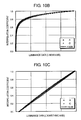
- Fig. 10B shows actually measured values (ideal values) of the luminance data S4 in pixel A and pixel C and interpolation coefficients according to the present embodiment, and a coefficient curve (lookup curve) acquired by a same method as the second and third steps of the first embodiment.
- plots of "pixel A” and “pixel B” are ideal values
- a plot of " ⁇ 0.98" is the coefficient curve.
- Fig. 10C is a graph in which the abscissa of Fig. 10B is changed from a linear scale to a logarithmic scale. In each drawing, ideal values and coefficient curves match in the entire luminance area. Therefore even in a PHM driven image display apparatus, luminance dispersion can be suppressed in the entire luminous area.
- the inclination of the coefficient curve changes dramatically in the boundary (gradation level n in Fig. 4A ) between the area in which the amplitude is modulated and the area in which the pulse width is modulated, but in the PHM of the present embodiment, the interpolation coefficient changes almost linearly with respect to the luminance (logarithmic axis). Therefore in the case of the present embodiment, a good correction result can be acquired by using the prepared logarithmic (or exponential) function as the coefficient curve, omitting the second step and third step. By omitting the second step and third step, the time required for measuring luminance can be further decreased.
- a fifth embodiment of the present invention will now be described with reference to Fig. 11A to Fig. 11C .
- the difference from the first embodiment will be described herein below.
- the modulation system of the present embodiment is a combination of amplitude modulation (PHM) and pulse width modulation (PWM).
- Fig. 11A shows a drive waveform of a signal line.
- the ordinate is the voltage value
- the abscissa is time
- the drive waveform in each gradation level (corresponds to S7 in Fig. 2A ) is shown side by side.
- the gradation levels are levels 0 to 128. In the range of gradation levels 1 to 32, the amplitude is 2.5 V, and the pulse width increases about 0.4 ⁇ sec each time.
- the waveform consists of a pulse with a 5 V amplitude, and a pulse with a 2.5 V amplitude is output, and the pulse width with the 5 V amplitude increases.
- a waveform consists of a pulse with a 7.5 V amplitude, and a pulse with the 5 V amplitude is output in the range of gradation levels 65 to 96
- a waveform consists of a pulse with a 10 V amplitude, and a pulse with a 7.5 V amplitude is output in the range of gradation levels 97 to 128.
- Vx 10 [V]
- Vy -8 [V]
- Vus 5 [V].
- the pulse width, number of gradation levels and voltage value or the like are not limited to these values, but can be arbitrarily designed.
- Fig. 11B shows actually measured values (ideal values) of the luminance data S4 in pixel A and pixel C and interpolation coefficients according to the present embodiment, and a coefficient curve (lookup table) acquired by a same method as the second and third steps of the first embodiment.
- plots of "pixel A” and “pixel B” are ideal values
- the plot of " ⁇ 0.98" is the coefficient curve.
- Fig. 11C is a graph in which the abscissa of Fig. 11B is changed from a linear scale to logarithmic scale. In each drawing, ideal values and coefficient curves match in the entire luminance area. Therefore even in an image display apparatus using a modulation system combining PHM and PWM, luminance dispersion can be suppressed in the entire luminance area.
- An image display apparatus of this example drives surface conduction type electron-emitting devices based on simple matrix driving using a PWM system with through rate control.
- the matrix panel 1 of this example has 240 rows of scan lines 1002, and 160 ⁇ 3 (RGB) columns of signal lines 1001.
- Fig. 2B shows, in the matrix panel 1a plurality of surface conduction type electron-emitting devices 1004 are arranged in a matrix, and each device is connected to the scan line 1002 and the signal line 1001 respectively.
- the measurement in the first step was performed using the drive signal in Fig. 6A . Also the measurements in the second step and third step were performed using the drive signals in Fig. 6B and Fig. 6C .
- the correction value (quantization data) in an average pixel is ⁇ 1.0 (127), with which quantization errors can be controlled to 1% or less. Even if about 2 bits of gradation are lost by correction, at least 10 bits can be secured for gradation after correction, so an image can be displayed in good condition.
- Fig. 12A shows a result of measuring luminance after correction according to this example.
- the abscissa is the luminance data S4 and the ordinate is the normalized luminance ratio of pixel A and pixel C, which was normalized by the luminance of pixel B for each gradation level. It is shown that the normalized luminance ratio is about 1 in the entire luminance data area. The luminance dispersion was hardly observed visually.
- the configuration of the correction unit is the same as the above example, except that the gradation level conversion circuit 210 is not disposed.
- Fig. 12B shows a result of measuring luminance after correction according to this comparison example.
- the abscissa is the luminous data S4 and the ordinate is the normalized luminance ratio of pixel A and pixel C, which was normalized by the luminance of pixel B for each gradation level. It is shown that interpolation errors in the mid-luminance data increases if the general linear interpolation in Fig. 12B is used, while the normalized luminance ratio is about 1 in the entire luminance data area in the case of the example in Fig. 12A .
- a first step drives a plurality of electron-emitting devices with a drive signal corresponding to a first gradation level and measures the luminance dispersion.
- a second step selects one or more electron-emitting devices as target devices, drives them with a drive signal corresponding to each gradation level, and measures their luminance for each gradation level.
- a third step drives the target devices with a drive signal having a voltage amplitude of a drive signal corresponding to each gradation level multiplied by a constant, and measures their luminance for each gradation level. Then, a correction value for each gradation level of each electron-emitting device is calculated using a luminance ratio of the luminance measured in the second step to the luminance measured in the third step, and the luminance dispersion measured in the first step.
Landscapes
- Engineering & Computer Science (AREA)
- Physics & Mathematics (AREA)
- Computer Hardware Design (AREA)
- General Physics & Mathematics (AREA)
- Theoretical Computer Science (AREA)
- Control Of Indicators Other Than Cathode Ray Tubes (AREA)
Applications Claiming Priority (1)
| Application Number | Priority Date | Filing Date | Title |
|---|---|---|---|
| JP2009092226A JP2010243775A (ja) | 2009-04-06 | 2009-04-06 | 補正値の取得方法、補正方法、画像表示装置 |
Publications (2)
| Publication Number | Publication Date |
|---|---|
| EP2239722A2 true EP2239722A2 (fr) | 2010-10-13 |
| EP2239722A3 EP2239722A3 (fr) | 2011-07-20 |
Family
ID=42536365
Family Applications (1)
| Application Number | Title | Priority Date | Filing Date |
|---|---|---|---|
| EP10155434A Withdrawn EP2239722A3 (fr) | 2009-04-06 | 2010-03-04 | Procédé d'acquisition de valeur de correction, procédé de correction et appareil d'affichage d'images |
Country Status (4)
| Country | Link |
|---|---|
| US (1) | US20100253709A1 (fr) |
| EP (1) | EP2239722A3 (fr) |
| JP (1) | JP2010243775A (fr) |
| CN (1) | CN101859526A (fr) |
Cited By (1)
| Publication number | Priority date | Publication date | Assignee | Title |
|---|---|---|---|---|
| WO2014140522A3 (fr) * | 2013-03-14 | 2014-12-18 | The University Court Of The University Of Edinburgh | Procédé de génération de niveaux de luminance prédéterminés sur un afficheur visuel électronique |
Families Citing this family (13)
| Publication number | Priority date | Publication date | Assignee | Title |
|---|---|---|---|---|
| KR101065406B1 (ko) * | 2010-03-25 | 2011-09-16 | 삼성모바일디스플레이주식회사 | 표시 장치, 영상 신호 보정 시스템, 및 영상 신호 보정 방법 |
| KR20140122362A (ko) * | 2013-04-09 | 2014-10-20 | 삼성디스플레이 주식회사 | 표시 장치 및 표시 장치의 구동 방법 |
| CN103559861B (zh) * | 2013-11-04 | 2016-06-29 | 苏州君嬴电子科技有限公司 | Led显示误差值获取系统及方法 |
| KR102159389B1 (ko) * | 2014-03-17 | 2020-09-24 | 삼성디스플레이 주식회사 | 디지털 비디오 데이터를 보정하기 위한 보정 데이터 산출방법과 이를 이용하여 생성한 룩-업 테이블을 포함하는 유기전계발광 표시장치 |
| US9530343B2 (en) | 2014-06-23 | 2016-12-27 | Shenzhen China Star Optoelectronics Technology Co., Ltd. | Method for correcting gray-scale of display panel |
| WO2016031006A1 (fr) * | 2014-08-28 | 2016-03-03 | Necディスプレイソリューションズ株式会社 | Dispositif d'affichage, dispositif de génération de carte de correction de gradation, procédé et programme pour la génération d'une carte de correction de gradation |
| JP7054577B2 (ja) * | 2017-11-20 | 2022-04-14 | シナプティクス インコーポレイテッド | 表示ドライバ、表示装置及びムラ補正方法 |
| CN107799084B (zh) * | 2017-11-21 | 2019-11-22 | 武汉华星光电半导体显示技术有限公司 | 亮度补偿的装置及方法、存储器 |
| KR102528532B1 (ko) * | 2018-08-23 | 2023-05-04 | 삼성전자주식회사 | 디스플레이 장치 및 그 휘도 제어 방법 |
| CN113870811B (zh) * | 2020-06-30 | 2022-12-30 | 武汉天马微电子有限公司 | 显示装置及其亮度调节方法、装置、电子设备及存储介质 |
| US12125441B2 (en) * | 2020-11-10 | 2024-10-22 | Sony Group Corporation | Light-emitting device, method of driving light- emitting device, and electronic apparatus |
| CN112233615B (zh) * | 2020-12-09 | 2021-03-05 | 卡莱特(深圳)云科技有限公司 | 一种提升led显示屏显示效果的方法及装置 |
| US11929007B2 (en) * | 2021-12-26 | 2024-03-12 | Novatek Microelectronics Corp. | Display driving integrated circuit and driving parameter adjustment method thereof |
Citations (5)
| Publication number | Priority date | Publication date | Assignee | Title |
|---|---|---|---|---|
| JP2000122598A (ja) | 1998-10-20 | 2000-04-28 | Matsushita Electric Ind Co Ltd | 表示装置 |
| US6097356A (en) | 1997-07-01 | 2000-08-01 | Fan; Nongqiang | Methods of improving display uniformity of thin CRT displays by calibrating individual cathode |
| EP1424672A1 (fr) | 2002-11-29 | 2004-06-02 | Barco N.V. | Procédé de commande et dispositif de correction des non-uniformités des pixels d'un dispositif d'affichage à matrice |
| US20060209215A1 (en) | 2004-06-18 | 2006-09-21 | Kabushiki Kaisha Toshiba | Video display device and luminance characteristic correcting method of video display device |
| US20070030215A1 (en) | 2005-08-08 | 2007-02-08 | Lee Ji W | Electron emission display device and control method of the same |
Family Cites Families (19)
| Publication number | Priority date | Publication date | Assignee | Title |
|---|---|---|---|---|
| US6621475B1 (en) * | 1996-02-23 | 2003-09-16 | Canon Kabushiki Kaisha | Electron generating apparatus, image forming apparatus, method of manufacturing the same and method of adjusting characteristics thereof |
| CN1377495A (zh) * | 1999-10-04 | 2002-10-30 | 松下电器产业株式会社 | 显示面板的驱动方法、显示面板的亮度校正装置及其驱动装置 |
| JP3673761B2 (ja) * | 2001-02-09 | 2005-07-20 | キヤノン株式会社 | 電子源の特性調整方法及び電子源の製造方法及び画像表示装置の特性調整方法及び画像表示装置の製造方法 |
| JP5022547B2 (ja) * | 2001-09-28 | 2012-09-12 | キヤノン株式会社 | 画像形成装置の特性調整方法、画像形成装置の製造方法、画像形成装置及び特性調整装置 |
| JP4115330B2 (ja) * | 2002-05-08 | 2008-07-09 | キヤノン株式会社 | 画像形成装置の製造方法 |
| JP4027284B2 (ja) * | 2002-07-26 | 2007-12-26 | キヤノン株式会社 | 画像表示装置の製造方法 |
| JP4012168B2 (ja) * | 2003-05-14 | 2007-11-21 | キヤノン株式会社 | 信号処理装置、信号処理方法、補正値生成装置、補正値生成方法及び表示装置の製造方法 |
| JP4047306B2 (ja) * | 2003-07-15 | 2008-02-13 | キヤノン株式会社 | 補正値の決定方法、表示装置の製造方法 |
| JP2005257791A (ja) * | 2004-03-09 | 2005-09-22 | Canon Inc | 画像表示装置及び画像表示装置の駆動方法 |
| JP4086852B2 (ja) * | 2004-03-16 | 2008-05-14 | キヤノン株式会社 | 画像表示装置 |
| JP2006017853A (ja) * | 2004-06-30 | 2006-01-19 | Canon Inc | 画像表示方法及び画像表示システム |
| JP4100379B2 (ja) * | 2004-08-09 | 2008-06-11 | セイコーエプソン株式会社 | 電気光学装置および電気光学装置の表示方法 |
| JP4222340B2 (ja) * | 2004-09-22 | 2009-02-12 | ソニー株式会社 | 画像表示装置および画像表示装置における輝度補正方法 |
| KR20060028919A (ko) * | 2004-09-30 | 2006-04-04 | 삼성에스디아이 주식회사 | 전자 방출 디스플레이 패널의 구동을 위한 계조 데이터를보정하는 방법 |
| JP2007199684A (ja) * | 2005-12-28 | 2007-08-09 | Canon Inc | 画像表示装置 |
| JP5130804B2 (ja) * | 2006-10-02 | 2013-01-30 | セイコーエプソン株式会社 | 発光装置および画像形成装置 |
| JP4926679B2 (ja) * | 2006-12-06 | 2012-05-09 | キヤノン株式会社 | 画像表示装置 |
| JP2008158285A (ja) * | 2006-12-25 | 2008-07-10 | Canon Inc | 画像表示装置 |
| JP2009008776A (ja) * | 2007-06-27 | 2009-01-15 | Canon Inc | 画像表示装置およびその製造方法 |
-
2009
- 2009-04-06 JP JP2009092226A patent/JP2010243775A/ja not_active Withdrawn
-
2010
- 2010-03-04 EP EP10155434A patent/EP2239722A3/fr not_active Withdrawn
- 2010-03-24 US US12/730,834 patent/US20100253709A1/en not_active Abandoned
- 2010-03-31 CN CN201010157705A patent/CN101859526A/zh active Pending
Patent Citations (5)
| Publication number | Priority date | Publication date | Assignee | Title |
|---|---|---|---|---|
| US6097356A (en) | 1997-07-01 | 2000-08-01 | Fan; Nongqiang | Methods of improving display uniformity of thin CRT displays by calibrating individual cathode |
| JP2000122598A (ja) | 1998-10-20 | 2000-04-28 | Matsushita Electric Ind Co Ltd | 表示装置 |
| EP1424672A1 (fr) | 2002-11-29 | 2004-06-02 | Barco N.V. | Procédé de commande et dispositif de correction des non-uniformités des pixels d'un dispositif d'affichage à matrice |
| US20060209215A1 (en) | 2004-06-18 | 2006-09-21 | Kabushiki Kaisha Toshiba | Video display device and luminance characteristic correcting method of video display device |
| US20070030215A1 (en) | 2005-08-08 | 2007-02-08 | Lee Ji W | Electron emission display device and control method of the same |
Cited By (1)
| Publication number | Priority date | Publication date | Assignee | Title |
|---|---|---|---|---|
| WO2014140522A3 (fr) * | 2013-03-14 | 2014-12-18 | The University Court Of The University Of Edinburgh | Procédé de génération de niveaux de luminance prédéterminés sur un afficheur visuel électronique |
Also Published As
| Publication number | Publication date |
|---|---|
| CN101859526A (zh) | 2010-10-13 |
| US20100253709A1 (en) | 2010-10-07 |
| EP2239722A3 (fr) | 2011-07-20 |
| JP2010243775A (ja) | 2010-10-28 |
Similar Documents
| Publication | Publication Date | Title |
|---|---|---|
| EP2239722A2 (fr) | Procédé d'acquisition de valeur de correction, procédé de correction et appareil d'affichage d'images | |
| KR101487548B1 (ko) | 표시 장치, 표시 장치의 제어 방법 및 컴퓨터 프로그램이 기록된 기록 매체 | |
| US8537081B2 (en) | Display apparatus and display control method | |
| US7227519B1 (en) | Method of driving display panel, luminance correction device for display panel, and driving device for display panel | |
| US7995080B2 (en) | Image display apparatus | |
| US8446437B2 (en) | Display device, method of driving display device, and program | |
| US20080049050A1 (en) | Image display apparatus | |
| KR20080101679A (ko) | 표시 장치, 영상 신호 처리 방법, 및 프로그램 | |
| CN101308625A (zh) | 显示装置、用于显示装置的驱动方法和计算机程序 | |
| US7379079B2 (en) | Electron emission device and driving method thereof | |
| US8289349B2 (en) | Correction method | |
| JP2000221945A (ja) | マトリクス型表示装置 | |
| JP2009053651A (ja) | 電子放出表示装置及び映像信号補正方法 | |
| JP2007199684A (ja) | 画像表示装置 | |
| US7773062B2 (en) | Method and apparatus for uniformity compensation in an electroluminescent display | |
| US20090002389A1 (en) | Image display apparatus and manufacturing method thereof | |
| JP2006309126A (ja) | 電子放出素子の駆動装置およびその駆動方法 | |
| US20090256866A1 (en) | Image display apparatus | |
| JP2001195026A (ja) | マトリクス型表示装置 | |
| US20050200319A1 (en) | Image display apparatus, drive method for the image display apparatus, and television set | |
| US20060001369A1 (en) | Image display method and image display device | |
| KR100902230B1 (ko) | 영상신호 보정방법 및 그를 이용한 전자방출표시장치 | |
| JP2012073362A (ja) | 表示装置及びその制御方法 | |
| JP2000148074A (ja) | マトリクス型表示装置 | |
| JP2006523858A (ja) | 表示装置 |
Legal Events
| Date | Code | Title | Description |
|---|---|---|---|
| PUAI | Public reference made under article 153(3) epc to a published international application that has entered the european phase |
Free format text: ORIGINAL CODE: 0009012 |
|
| AK | Designated contracting states |
Kind code of ref document: A2 Designated state(s): AT BE BG CH CY CZ DE DK EE ES FI FR GB GR HR HU IE IS IT LI LT LU LV MC MK MT NL NO PL PT RO SE SI SK SM TR |
|
| AX | Request for extension of the european patent |
Extension state: AL BA ME RS |
|
| PUAL | Search report despatched |
Free format text: ORIGINAL CODE: 0009013 |
|
| AK | Designated contracting states |
Kind code of ref document: A3 Designated state(s): AT BE BG CH CY CZ DE DK EE ES FI FR GB GR HR HU IE IS IT LI LT LU LV MC MK MT NL NO PL PT RO SE SI SK SM TR |
|
| AX | Request for extension of the european patent |
Extension state: AL BA ME RS |
|
| 17P | Request for examination filed |
Effective date: 20120120 |
|
| STAA | Information on the status of an ep patent application or granted ep patent |
Free format text: STATUS: THE APPLICATION HAS BEEN WITHDRAWN |
|
| 18W | Application withdrawn |
Effective date: 20120614 |