EP2240002A2 - Appareil de montage électronique destiné au fonctionnement d'au moins deux types différents de lampes à décharge - Google Patents
Appareil de montage électronique destiné au fonctionnement d'au moins deux types différents de lampes à décharge Download PDFInfo
- Publication number
- EP2240002A2 EP2240002A2 EP10156476A EP10156476A EP2240002A2 EP 2240002 A2 EP2240002 A2 EP 2240002A2 EP 10156476 A EP10156476 A EP 10156476A EP 10156476 A EP10156476 A EP 10156476A EP 2240002 A2 EP2240002 A2 EP 2240002A2
- Authority
- EP
- European Patent Office
- Prior art keywords
- voltage
- value
- output
- boost converter
- peak
- Prior art date
- Legal status (The legal status is an assumption and is not a legal conclusion. Google has not performed a legal analysis and makes no representation as to the accuracy of the status listed.)
- Withdrawn
Links
Images

Classifications
-
- H—ELECTRICITY
- H05—ELECTRIC TECHNIQUES NOT OTHERWISE PROVIDED FOR
- H05B—ELECTRIC HEATING; ELECTRIC LIGHT SOURCES NOT OTHERWISE PROVIDED FOR; CIRCUIT ARRANGEMENTS FOR ELECTRIC LIGHT SOURCES, IN GENERAL
- H05B41/00—Circuit arrangements or apparatus for igniting or operating discharge lamps
- H05B41/14—Circuit arrangements
- H05B41/26—Circuit arrangements in which the lamp is fed by power derived from DC by means of a converter, e.g. by high-voltage DC
- H05B41/28—Circuit arrangements in which the lamp is fed by power derived from DC by means of a converter, e.g. by high-voltage DC using static converters
- H05B41/282—Circuit arrangements in which the lamp is fed by power derived from DC by means of a converter, e.g. by high-voltage DC using static converters with semiconductor devices
- H05B41/2825—Circuit arrangements in which the lamp is fed by power derived from DC by means of a converter, e.g. by high-voltage DC using static converters with semiconductor devices by means of a bridge converter in the final stage
-
- H—ELECTRICITY
- H05—ELECTRIC TECHNIQUES NOT OTHERWISE PROVIDED FOR
- H05B—ELECTRIC HEATING; ELECTRIC LIGHT SOURCES NOT OTHERWISE PROVIDED FOR; CIRCUIT ARRANGEMENTS FOR ELECTRIC LIGHT SOURCES, IN GENERAL
- H05B41/00—Circuit arrangements or apparatus for igniting or operating discharge lamps
- H05B41/14—Circuit arrangements
- H05B41/36—Controlling
Definitions
- the present invention relates to an electronic ballast for operating at least two different types of discharge lamps, the operation of which requires a different lamp current, comprising: an input having a first and a second input terminal for connecting a DC supply voltage, a boost converter having a boost choke, a boost switch having a control electrode, a reference electrode and a working electrode, and a boost diode, the boost converter coupled on the input side between the first and second input terminals and having an output having a first and a second output terminal, a bridge circuit having a first and a second electronic switch, wherein the first and the second electronic switch each having a control electrode, a reference electrode and a working electrode, wherein the series connection of the first and the second electronis coupled to a first bridge center between the first and the second output terminal of the boost converter, an output having a first and a second output terminal for connecting the discharge lamp, wherein the first output terminal is coupled to the first bridge center and wherein the second output terminal is coupled to the second output terminal of the rectifier, a lamp inductor
- the condition for a sinusoidal current consumption is met, is used as a circuit typology primarily a boost converter in the mains input.
- the output voltage of the boost converter the so-called intermediate circuit voltage
- the maximum peak value is approximately 372 V.
- the DC link voltage is set to be a fixed percentage, for example 15%, above the maximum peak value of the mains input voltage.
- the intermediate circuit voltage is approx.
- the object of the present invention is to further develop an electronic ballast mentioned at the beginning in such a way that low-loss operation is possible with as little electromagnetic interference as possible.
- the present invention is based on the finding that the mains input voltage and the intermediate circuit voltage can be determined by the boost converter at the same time using a microcontroller.
- the DC link voltage can now be regulated be that it is a certain percentage, for example 4% to 8%, above the peak value of the mains input voltage.
- the intermediate circuit voltage is thus lowered, and the intermediate circuit voltage is increased to the same extent when the mains input voltage is increased.
- the microcontroller is configured to regulate the voltage between the first and second output terminals of the boost converter to be at least within a first range of the voltage value of the peak of the voltage between the first and second input terminals or within a first range of the voltage value between the first and the second output terminal of the boost converter, a predeterminable threshold is above the voltage value of the peak of the voltage between the first and the second input terminal.
- a predeterminable threshold is above the voltage value of the peak of the voltage between the first and the second input terminal.
- the voltage at the input or the voltage at the output of the boost converter is measured and ensured by appropriate control of the switch of the boost converter that the output voltage of the boost converter is always so large that safely a sinusoidal current consumption is effected on the other hand, however, is small enough to minimize the losses.
- the low voltage swing between the voltage at the input and the voltage at the output of the boost converter increases the efficiency of the boost converter.
- the current load in the Reduced components of an electronic ballast according to the invention so that smaller components can be used. This reduces the price of the components and their space requirements. Due to the lower average output voltage of the boost converter compared to the prior art, the losses in the boost converter are significantly reduced.
- the predefinable threshold is in particular between 2% and 10%, preferably between 4% and 8%, of the voltage value of the summit of the voltage between the first and the second input connection. While in the prior art for security reasons, the threshold has been constant 15% above the maximum voltage value of the peak of the voltage between the first and the second input terminal, according to the invention results in a much smaller distance and thus a significant reduction in losses.
- a particularly preferred category of further developments is characterized in that the microcontroller is further designed to determine the type of discharge lamp connected to the output by passing through a measuring routine, wherein in the microcontroller for each of the at least two types of discharge lamps a lower limit for the first Value range of the voltage value of the peak of the voltage between the first and the second input terminal or a lower limit for the first value range of the voltage value between the first and the second output terminal of the boost converter is stored.
- the type of discharge lamp is preferably represented by the nominal value of its lamp current and / or the nominal value of its lamp power.
- the microcontroller is particularly preferably designed in a second range of values which is below the lower limit value for the first value range of the voltage value of the peak of the voltage between the first and the second input terminal or in a second value range which is below the upper limit value for connecting the first value range of the voltage value between the first and the second output terminal of the boost converter, by varying the switching frequency of the signal provided at the third output to regulate the voltage between the first and the second output terminal of the boost converter to a minimum voltage.
- This measure takes into account the fact that when operating discharge lamps, the distance between the voltage value of the summit of the voltage at the input and the voltage at the output of the boost converter can not be regulated to the predefinable threshold over the entire value range.
- the minimum voltage is preferably at least as great as the lower limit value of the first value range of the voltage between the first and the second output connection of the boost converter, in particular the minimum voltage corresponds to this lower limit value. This maximizes the reduction in losses while ensuring the operation of the particular type of lamp.
- Fig. 1 shows a schematic representation of an embodiment of an electronic ballast according to the invention. It comprises an input with a first and a second input connection, between which a mains voltage U N is applied.
- a rectifier 10 is coupled to the input, to whose output E1, E2 a voltage U gl is provided which corresponds to the rectified mains voltage U N.
- the voltage U gl has a peak value U peak .
- the rectifier 10 is followed by a boost converter 12 which comprises a boost inductor L1, a boost diode D1 and a boost switch S1.
- a DC voltage could also be connected directly to the input of the boost converter 12.
- the electronic ballast according to the invention would thus work the same way.
- the voltage provided at the output of the boost converter 12, stabilized by means of a capacitor C1, is the so-called intermediate circuit voltage U Zw .
- a bridge circuit is coupled, which in the present case comprises the switches S2 and S3.
- a bridge center BM1 is defined.
- the series circuit of a coupling capacitor C K and a lamp inductor L2 is coupled.
- the first output terminal A1 acts as a second bridge center BM2.
- a resonance capacitor C res is coupled, on the other hand, the discharge lamp La.
- the electronic ballast has a microcontroller 14, which controls the switches S2 and S3 by means of signals provided at its outputs AM1 and AM2. These signals are characterized by a current frequency f 23 . Via an output AM3, the microcontroller 14 controls the switch S1, wherein the signal provided at the output AM3 is characterized by a current frequency f 1 . This is done in the present case in that the micro-controller 14 provides an ON-time at its output AM3, wherein the frequency f 1 is automatically results from the time required for the current in the boost inductor L1 to be zero again.
- a first input EM1 which is coupled to the tap of a voltage divider R1, R2, the microcontroller 14 is coupled to a signal which is correlated with the voltage U gl .
- the Microcontroller 14 via its input EM2, which is coupled to the tap of a voltage divider R3, R4, coupled to a signal which is correlated with the intermediate circuit voltage U Zw .
- a shunt resistor R Sh is furthermore arranged in series with the discharge lamp La, the voltage dropping across the shunt resistor R Sh being supplied to the microcontroller 14 via an input EM3, wherein the microcontroller 14 is designed to supply the output current I La by corresponding Variation of the signals AM1, AM2, as known to those skilled to vary.
- the microcontroller 14 is designed to control the switch S1 by setting the frequency f 1 such that the voltage U Zw always lies within a first value range of the peak value U peak of the voltage U gl a predeterminable threshold above the value of U peak .
- This predefinable threshold is preferably between 2% and 10%, in particular between 4% and 8%, of the voltage value of U peak .
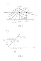
- Fig. 2 shows the course of the lamp current I La as a function of the frequency f 23 , that is the frequency of the signals at the outputs AM1, AM2 of the microcontroller 14, which serve to drive the switches S2, S3. Shown are three curves that stand for different DC link voltages U Zw . The lowest curve corresponds to an intermediate circuit voltage U Zw equal to 270 V, the middle curve corresponds to an intermediate circuit voltage U zw equal to 370 V and the uppermost curve corresponds to an intermediate circuit voltage U Zw equal to 430 V. Note that due to the inductive nature of the load, the electronic Ballast in the sloping area of the respective curve train of U Zw is to operate.
- the lamp must be operated at the operating point P1, that is, the microcontroller 14 selects one here Frequency f 23 of 70 kHz.
- a correspondingly smaller intermediate circuit voltage can be set by appropriate activation of the switch S1, that is to say by selecting the frequency f 1 U Zw equal to 370 V.
- the switch S1 For setting a lamp current of I La equal to 300 mA, the lamp La is operated at the operating point P2, that is f 23 is 30 kHz.
- the mains voltage U N now drops to even lower values, then U gl at the output of the rectifier 10 also drops.
- the intermediate circuit voltage U Zw is lowered accordingly, for example to U Zw equal to 270 V, then the illustration of FIG Fig. 2 that no operating point can be found in which the lamp la can be operated with the required lamp current I La of 300 mA.
- Fig. 3 shows for a particularly preferred embodiment, the dependence of the intermediate circuit voltage U Zw of the voltage U peak , that is, the voltage value of the summit of the voltage U gl at the input of the boost converter 12.
- U ZW a , U peak . where a > 1.
- a is between 1.02 and 1.10.
- the minimum intermediate circuit voltage is defined by U Zwmin , which is dependent on the type of lamp La, which is connected to the output A1, A2 of the electronic ballast, set to reach the Lampenennnstrom.
- Corresponding values of the lamp nominal current or the lamp power and / or the minimum intermediate circuit voltage U Zwmin can be stored for various lamp types in the microcontroller 14, for example in the form of a look-up table.
- the value U Zwmin can still be made dependent on other boundary conditions, for example, whether the electronic ballast is fed directly from a DC voltage source or from an AC voltage source, as in the embodiment of Fig. 1 , as well as the resulting frequency f 23 .
Landscapes
- Circuit Arrangements For Discharge Lamps (AREA)
Applications Claiming Priority (1)
| Application Number | Priority Date | Filing Date | Title |
|---|---|---|---|
| DE200910016906 DE102009016906A1 (de) | 2009-04-08 | 2009-04-08 | Elektronisches Vorschaltgerät zum Betreiben von mindestens zwei unterschiedlichen Typen von Entladungslampen |
Publications (2)
| Publication Number | Publication Date |
|---|---|
| EP2240002A2 true EP2240002A2 (fr) | 2010-10-13 |
| EP2240002A3 EP2240002A3 (fr) | 2016-11-30 |
Family
ID=42335161
Family Applications (1)
| Application Number | Title | Priority Date | Filing Date |
|---|---|---|---|
| EP10156476.3A Withdrawn EP2240002A3 (fr) | 2009-04-08 | 2010-03-15 | Appareil de montage électronique destiné au fonctionnement d'au moins deux types différents de lampes à décharge |
Country Status (4)
| Country | Link |
|---|---|
| EP (1) | EP2240002A3 (fr) |
| KR (1) | KR20100112097A (fr) |
| CN (1) | CN101861041B (fr) |
| DE (1) | DE102009016906A1 (fr) |
Family Cites Families (8)
| Publication number | Priority date | Publication date | Assignee | Title |
|---|---|---|---|---|
| JP2587710B2 (ja) * | 1990-04-28 | 1997-03-05 | 株式会社小糸製作所 | 車輌用放電灯の点灯回路 |
| EP1442633A1 (fr) * | 2001-10-29 | 2004-08-04 | Koninklijke Philips Electronics N.V. | Circuit de ballast |
| AU2002349518A1 (en) * | 2001-11-27 | 2003-06-10 | Matsushita Electric Works, Ltd. | Electronic ballast for high-pressure discharge lamp |
| US7075254B2 (en) * | 2004-12-14 | 2006-07-11 | Lutron Electronics Co., Inc. | Lighting ballast having boost converter with on/off control and method of ballast operation |
| CN2884788Y (zh) * | 2006-01-24 | 2007-03-28 | 上海瓯宝电子科技有限公司 | 带输出电路保护的汽车用hid灯镇流器 |
| US7365951B2 (en) * | 2006-03-07 | 2008-04-29 | Matsushita Electric Works, Ltd. | Discharge lamp lighting device, lighting system and method |
| CN200947697Y (zh) * | 2006-09-19 | 2007-09-12 | 李英 | Hid灯热启动的电子镇流装置 |
| CN200950692Y (zh) * | 2006-09-19 | 2007-09-19 | 永益开发有限公司 | 用于高压气体放电灯的电子镇流器 |
-
2009
- 2009-04-08 DE DE200910016906 patent/DE102009016906A1/de not_active Withdrawn
-
2010
- 2010-03-15 EP EP10156476.3A patent/EP2240002A3/fr not_active Withdrawn
- 2010-04-08 CN CN201010149925.4A patent/CN101861041B/zh not_active Expired - Fee Related
- 2010-04-08 KR KR1020100032201A patent/KR20100112097A/ko not_active Withdrawn
Non-Patent Citations (1)
| Title |
|---|
| None |
Also Published As
| Publication number | Publication date |
|---|---|
| DE102009016906A1 (de) | 2010-10-21 |
| KR20100112097A (ko) | 2010-10-18 |
| CN101861041B (zh) | 2014-12-10 |
| CN101861041A (zh) | 2010-10-13 |
| EP2240002A3 (fr) | 2016-11-30 |
Similar Documents
| Publication | Publication Date | Title |
|---|---|---|
| EP1603219B1 (fr) | Procédé et dispositif pour la correction du facteur de puissance | |
| EP0876742B1 (fr) | Procede et circuit de commande electronique pour la regulation des caracteristiques de fonctionnement de lampes a decharge | |
| DE102005006587B4 (de) | Wechselrichter insbesondere für eine konstante Lichtabgabe einer Kaltkathodenfluoreszenzlampe und Verfahren zum Betrieb dieses Wechselrichters | |
| EP1872627B1 (fr) | Pfc numerique parametrable | |
| DE102008027029A1 (de) | Lampentyperkennung durch Leistungsfaktorkorrekturschaltung | |
| EP1227705A2 (fr) | Ballast pour lampes comprenant un convertisseur du type SEPIC | |
| DE102009047632B4 (de) | Schaltungsanordnung zum Betreiben mindestens einer LED | |
| EP2138015B1 (fr) | Circuit permettant de produire une tension auxiliaire et de faire fonctionner au moins une lampe à décharge | |
| EP1492393B1 (fr) | Circuit et méthode pour alimenter une lampe à décharge muni d'une détection de fin de durée de vie | |
| EP2368410B1 (fr) | Procédé et ballast pour le fonctionnement d'un moyen d'éclairage avec un courant régulé | |
| EP0738455B1 (fr) | Dispositif servant au fonctionnement d'une lampe a decharge | |
| EP1424881B1 (fr) | Dispositif et méthode pour commander une lampe fluorescente | |
| EP2327276A1 (fr) | Montage et procédé de fonctionnement d'une lampe à décharge | |
| EP1732364B1 (fr) | Circuit et procédé de commande de puissance d'un ballast électronique en fonction de la tension de réseau | |
| EP2421336B1 (fr) | Ballast électronique destiné au fonctionnement d'au moins une lampe à décharge | |
| EP1994805B1 (fr) | Ensemble circuit et procédé pour faire fonctionner une lampe à décharge haute pression | |
| DE19613257A1 (de) | Verfahren und elektronische Steuerschaltung zum Regeln des Betriebsverhaltens von Gasentladungslampen | |
| EP2474206B1 (fr) | Correction de cosinus (phi) dans des ballasts à régulation du courant ou de la puissance pour des lampes | |
| DE102009016906A1 (de) | Elektronisches Vorschaltgerät zum Betreiben von mindestens zwei unterschiedlichen Typen von Entladungslampen | |
| EP2425684B1 (fr) | Circuit de ballast régulé en puissance pour un luminaire, et procédé de fonctionnement | |
| EP2849538B1 (fr) | Dispositif et procédé de détermination indirecte d'une alimentation électrique | |
| EP1793655B1 (fr) | Ballast électronique avec dispositif de surveillance de l'état de fonctionnement | |
| DE10127135B4 (de) | Dimmbares elektronisches Vorschaltgerät | |
| EP1732365A2 (fr) | Circuit et méthode pour détecter le facteur de forme d' un courant à travers une lampe ou d' une tension aux bornes d' une lampe | |
| EP2208401A1 (fr) | Ballast électronique et procédé pour faire fonctionner au moins une première et une deuxième lampes à décharge |
Legal Events
| Date | Code | Title | Description |
|---|---|---|---|
| PUAI | Public reference made under article 153(3) epc to a published international application that has entered the european phase |
Free format text: ORIGINAL CODE: 0009012 |
|
| AK | Designated contracting states |
Kind code of ref document: A2 Designated state(s): AT BE BG CH CY CZ DE DK EE ES FI FR GB GR HR HU IE IS IT LI LT LU LV MC MK MT NL NO PL PT RO SE SI SK SM TR |
|
| AX | Request for extension of the european patent |
Extension state: AL BA ME RS |
|
| RAP1 | Party data changed (applicant data changed or rights of an application transferred) |
Owner name: OSRAM AG |
|
| RAP1 | Party data changed (applicant data changed or rights of an application transferred) |
Owner name: OSRAM GMBH |
|
| RAP1 | Party data changed (applicant data changed or rights of an application transferred) |
Owner name: OSRAM GMBH |
|
| PUAL | Search report despatched |
Free format text: ORIGINAL CODE: 0009013 |
|
| AK | Designated contracting states |
Kind code of ref document: A3 Designated state(s): AT BE BG CH CY CZ DE DK EE ES FI FR GB GR HR HU IE IS IT LI LT LU LV MC MK MT NL NO PL PT RO SE SI SK SM TR |
|
| AX | Request for extension of the european patent |
Extension state: AL BA ME RS |
|
| RIC1 | Information provided on ipc code assigned before grant |
Ipc: H05B 41/36 20060101ALI20161021BHEP Ipc: H05B 41/282 20060101ALI20161021BHEP Ipc: H05B 41/24 20060101AFI20161021BHEP |
|
| 17P | Request for examination filed |
Effective date: 20170530 |
|
| RBV | Designated contracting states (corrected) |
Designated state(s): AT BE BG CH CY CZ DE DK EE ES FI FR GB GR HR HU IE IS IT LI LT LU LV MC MK MT NL NO PL PT RO SE SI SK SM TR |
|
| 17Q | First examination report despatched |
Effective date: 20180703 |
|
| GRAP | Despatch of communication of intention to grant a patent |
Free format text: ORIGINAL CODE: EPIDOSNIGR1 |
|
| INTG | Intention to grant announced |
Effective date: 20190625 |
|
| STAA | Information on the status of an ep patent application or granted ep patent |
Free format text: STATUS: THE APPLICATION IS DEEMED TO BE WITHDRAWN |
|
| 18D | Application deemed to be withdrawn |
Effective date: 20191106 |