EP2240889B1 - Objet portable à dispositif d'autocommutation - Google Patents
Objet portable à dispositif d'autocommutation Download PDFInfo
- Publication number
- EP2240889B1 EP2240889B1 EP09708354.7A EP09708354A EP2240889B1 EP 2240889 B1 EP2240889 B1 EP 2240889B1 EP 09708354 A EP09708354 A EP 09708354A EP 2240889 B1 EP2240889 B1 EP 2240889B1
- Authority
- EP
- European Patent Office
- Prior art keywords
- circuit
- power
- battery
- switching circuit
- electromagnetic field
- Prior art date
- Legal status (The legal status is an assumption and is not a legal conclusion. Google has not performed a legal analysis and makes no representation as to the accuracy of the status listed.)
- Active
Links
Images

Classifications
-
- G—PHYSICS
- G06—COMPUTING OR CALCULATING; COUNTING
- G06K—GRAPHICAL DATA READING; PRESENTATION OF DATA; RECORD CARRIERS; HANDLING RECORD CARRIERS
- G06K19/00—Record carriers for use with machines and with at least a part designed to carry digital markings
- G06K19/06—Record carriers for use with machines and with at least a part designed to carry digital markings characterised by the kind of the digital marking, e.g. shape, nature, code
- G06K19/067—Record carriers with conductive marks, printed circuits or semiconductor circuit elements, e.g. credit or identity cards also with resonating or responding marks without active components
- G06K19/07—Record carriers with conductive marks, printed circuits or semiconductor circuit elements, e.g. credit or identity cards also with resonating or responding marks without active components with integrated circuit chips
- G06K19/0723—Record carriers with conductive marks, printed circuits or semiconductor circuit elements, e.g. credit or identity cards also with resonating or responding marks without active components with integrated circuit chips the record carrier comprising an arrangement for non-contact communication, e.g. wireless communication circuits on transponder cards, non-contact smart cards or RFIDs
-
- G—PHYSICS
- G06—COMPUTING OR CALCULATING; COUNTING
- G06K—GRAPHICAL DATA READING; PRESENTATION OF DATA; RECORD CARRIERS; HANDLING RECORD CARRIERS
- G06K19/00—Record carriers for use with machines and with at least a part designed to carry digital markings
- G06K19/06—Record carriers for use with machines and with at least a part designed to carry digital markings characterised by the kind of the digital marking, e.g. shape, nature, code
- G06K19/067—Record carriers with conductive marks, printed circuits or semiconductor circuit elements, e.g. credit or identity cards also with resonating or responding marks without active components
- G06K19/07—Record carriers with conductive marks, printed circuits or semiconductor circuit elements, e.g. credit or identity cards also with resonating or responding marks without active components with integrated circuit chips
- G06K19/0701—Record carriers with conductive marks, printed circuits or semiconductor circuit elements, e.g. credit or identity cards also with resonating or responding marks without active components with integrated circuit chips at least one of the integrated circuit chips comprising an arrangement for power management
-
- G—PHYSICS
- G06—COMPUTING OR CALCULATING; COUNTING
- G06K—GRAPHICAL DATA READING; PRESENTATION OF DATA; RECORD CARRIERS; HANDLING RECORD CARRIERS
- G06K19/00—Record carriers for use with machines and with at least a part designed to carry digital markings
- G06K19/06—Record carriers for use with machines and with at least a part designed to carry digital markings characterised by the kind of the digital marking, e.g. shape, nature, code
- G06K19/067—Record carriers with conductive marks, printed circuits or semiconductor circuit elements, e.g. credit or identity cards also with resonating or responding marks without active components
- G06K19/07—Record carriers with conductive marks, printed circuits or semiconductor circuit elements, e.g. credit or identity cards also with resonating or responding marks without active components with integrated circuit chips
- G06K19/0701—Record carriers with conductive marks, printed circuits or semiconductor circuit elements, e.g. credit or identity cards also with resonating or responding marks without active components with integrated circuit chips at least one of the integrated circuit chips comprising an arrangement for power management
- G06K19/0702—Record carriers with conductive marks, printed circuits or semiconductor circuit elements, e.g. credit or identity cards also with resonating or responding marks without active components with integrated circuit chips at least one of the integrated circuit chips comprising an arrangement for power management the arrangement including a battery
- G06K19/0705—Record carriers with conductive marks, printed circuits or semiconductor circuit elements, e.g. credit or identity cards also with resonating or responding marks without active components with integrated circuit chips at least one of the integrated circuit chips comprising an arrangement for power management the arrangement including a battery the battery being connected to a power saving arrangement
Definitions
- the invention relates to a portable object with a self-switching device. More particularly, the self-switching device is used to switch on the power to the device at a given time with no human intervention.
- the portable object referred to in this document comprises at least one electronic circuit and a battery to power the said circuit.
- its operating time depends on the power consumed by the device and the battery charge capacity.
- the charging capacity of a battery is proportional with its size.
- a continuously operating device with a standby mode with lower power consumption may be used.
- the standby mode can sometimes use a large quantity of battery power. For example, if you consider a company access card that communicates using a radiofrequency communication protocol of the Wi-Fi, Bluetooth, HiperLAN or other type, the standby mode required for detecting communication requires powering an input amplifier with fairly high power needs. Even if the standby mode helps save the power consumed by the device, that is not enough for a battery with a very small capacity such as those found in credit-card sized cards. That is why a solution was required for further reducing the consumption of such devices.
- NFC Near Field Communication
- the European Patent Application EP 1 126 407 A2 discloses a data token with power saving switch. When a frequency selector senses R.F. input signals of the correct frequency, the power switch is activated and a battery is electrically connected to the token operational circuitry.
- the International Patent Application WO 99/52061 discloses a smart card with a power saving arrangement.
- a card triggering receiver powered by a battery, detects the emissions of triggering station and generates a signal for commanding closure of the power switch. Closure of the power switch provides power to the components of the smart card.
- US Patent US 6,593,845 B1 discloses a wake up circuit for a transponder using flip-flop to couple and to cut off the battery voltage to or from the main circuit.
- the invention proposes a battery-powered device, the powering of which is triggered by detecting an electromagnetic field.
- the power may be fully shut down as long as no field is detected.
- the invention relates to a portable electronic device according to claim 1.
- the electromagnetic field detection circuit may be self powered by the electromagnetic field.
- the magnetic field detection circuit can power the switching circuit during at least one phase of the start of the supply of power.
- the field detection circuit may have a resonant circuit and a rectification and regulation circuit.
- the resonant circuit is associated with a frequency range so that alternating voltage is created at its terminals in the presence of an electromagnetic field with a frequency located within the frequency range.
- the rectification and regulation circuit transforms the alternating voltage into direct voltage.
- the switching circuit may have a pushbutton to start the supply of power to the electronic circuit from the battery.
- the switching circuit may comprise an input connected to the electronic circuit to trigger the cutting off of the power to the said electronic circuit.
- the switching circuit may be an electronic relay.
- the switching circuit may comprise a transistor and a latch. The transistor is used to establish or cut off the power supply voltage to the electronic circuit.
- the latch is of the bistable type to control the transistor, and is powered self-selectively by the battery and the electromagnetic field detection circuit.
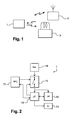
- FIG. 1 represents a portable electronic device 1 in its environment of use.
- the portable device 1 is for example a card designed to communicate by radiofrequency with a base station 2.
- the card is designed for a person moving inside a company, to whom information is to be sent about the jobs they need to carry out.
- the company further has access control terminals 3 for recording the passages of the person.
- the checking time is very brief and does not make it possible to exchange more than an identifier to check whether or not that person is authorised.
- the terminals 3 may also be used for other uses independent of cards 1, the key feature being that the terminals 3 emit an electromagnetic field that is sufficiently great to be detected, and for example compliant with a standard of the NFC type, e.g. ISO/IEC 14443.
- the card 1 may comprise a microcontroller 10, a user interface 11, a radiofrequency interface 12, a proximity communication interface 13, a battery 14 and a switching circuit 15.
- the microcontroller 10 is typically made up of at least one microprocessor and at least one memory that implement at least one program to control all the elements 11 to 14 that make up the card 1.
- the user interface 11 enables the card to interact with a user.
- the user interface may comprise a small LCD screen that may be integrated into a card of the credit-card size, a beep generator to report that a message has arrived, a fingerprint reader or a mini keypad.
- the radiofrequency interface 12 is a communication interface with a range located from a few dozen to a few hundred metres.
- the radiofrequency interface 12 is for instance compliant with one of the following standards - Bluetooth (IEEE 802.15.3), Zigbee (IEEE 802.15.4), Wi-Fi (IEEE 802.11) or other standards.
- the proximity communication interface 13 is an interface that may comply with standard ISO 14443. However, in the invention and as detailed below, the interface may be limited to the part relating to the recovery of power.
- the battery 14 is a small battery, thus offering a small capacity.
- the switching circuit 15 is used to connect the battery to the elements of the card 1 or otherwise, with the exception of the NFC interface 13, which has its own power supply.
- Figure 3 particularly details the part relating to the power supply of card 1.
- the interface NFC 13 is reduced here to its part concerning the recovery of power. For the invention, it is not necessary to have an electromagnetic field modulation/demodulation circuit.
- the NFC interface 13 has a resonant circuit that is made up of inductor Lr and a capacitance Cr tuned, for example, to a frequency of 13.56 MHz which is that of the access control terminals.
- the resonant circuit is coupled to a diode D 1 that has the task of rectifying the signal.
- a capacitor Cf then filters the signal supplied by diode D 1 .
- a Zener diode Dz in parallel on the capacitor Cf regulates the rectified and filtered voltage so that it is within a frequency range that is compatible with the power supply of an integrated circuit.
- This type of NCF interface 13 is well known to the man of the art and different variants are possible.
- the switching circuit 15 is an electronic relay.
- a transistor T is used to connect the positive terminal of the battery 14 through its channel to a power output of the switching circuit 15 to supply the Vcc power supply voltage to the other elements of the card 1.
- a bistable latch B of the SR (Set-Reset) type is connected to the gate of the transistor T to make it conduct or not through a control transistor Tc.
- the bistable latch is powered both by the NFC interface and by the Vcc power supply voltage through two diodes D 2 and D 3 . In that way, when the channel of transistor T is open, the latch B must be powered by the diode D2 and the NFC interface to operate. If the transistor T is shut, the latch B is powered by the diode D3 and the battery 14.
- the latch can maintain a 1 output status, making the control transistor Tc and transistor T conduct. If ever the output status of the latch switches to 0, the control transistor Tc is blocked and the leakage current from the transistor gate brings it to the same potential as its substrate, thus blocking transistor T. When transistor T is blocked, the battery 14 is disconnected from the other elements of the card 1.
- an input S of the latch B is connected to the Vdd potential supplied by the interface NFC 13.
- the input S is an input that sets the latch B to 1. In that way, as soon as the voltage Vdd reaches a level sufficient to power latch B, its output is set automatically to 1.
- the switching of transistor T maintains that level on 1 when the Vdd voltage drops, particularly because the movement of the card makes the level of the electronic magnetic field drop too low to supply sufficient power to power latch B.
- an input R of latch B is connected to an output of microcontroller 10.
- the input R is a latch B resetting input.
- the microcontroller output just has to be kept at 0 as long as the card is to be powered.
- Switching to 1 may be triggered by the microcontroller after a predefined time during which the card is idle, i.e. when there is no exchange of messages via the RF interface 12 or no action is taken from the user interface 1.
- Switching input R to one sets the output of latch B to zero, and thus blocks the control transistor Tc and transistor T, thereby cutting off the power supply to all the elements of card 1.
- the switching circuit 15 behaves like a bistable electromechanical relay that sets a switch to the open or closed position depending on two set voltages. However, in view of the small size of credit-card sized cards, it is preferable to have the described circuit, which can be integrated on an integrated circuit.
- a pushbutton BP that connects the output of the battery to the voltage input from the NFC interface.
- the power supply to the card can be started in the absence of the electromagnetic field by pressing the pushbutton BP.
- the pressure applied in this way simulates the entry into an electromagnetic field by the card.
- the switching circuit 15 switches the voltage supplied by the battery depending on two control signals, one of which comes from the detection of an electromagnetic field.
- the man of the art may note that the offered circuit is not powered when the battery is cut off, which has an added advantage for the previously presented mode of embodiment.
Landscapes
- Engineering & Computer Science (AREA)
- Computer Hardware Design (AREA)
- Microelectronics & Electronic Packaging (AREA)
- Physics & Mathematics (AREA)
- General Physics & Mathematics (AREA)
- Theoretical Computer Science (AREA)
- Computer Networks & Wireless Communication (AREA)
- Near-Field Transmission Systems (AREA)
- Mobile Radio Communication Systems (AREA)
- Electronic Switches (AREA)
- Communication Control (AREA)
- Power Sources (AREA)
- Charge And Discharge Circuits For Batteries Or The Like (AREA)
- Credit Cards Or The Like (AREA)
Claims (8)
- Dispositif électronique portable (1) comprenant une batterie (14) couplée à un circuit électronique (10 à 12) par l'intermédiaire d'un circuit de commutation (15) qui permet l'activation ou la désactivation d'une tension d'alimentation (Vcc) vers le circuit électronique utilisant la batterie, caractérisé en ce que le dispositif comprend en outre au moins un circuit de détection de champ électromagnétique (13) couplé au circuit de commutation (15) pour débuter la fourniture de puissance au circuit électronique (10 à 12) si un champ électromagnétique est détecté et dans lequel le circuit de commutation comprend une bascule bistable (B) pour maintenir la tension d'alimentation (Vcc), dans lequel ladite bascule (B) est alimentée par la batterie lorsque la tension d'alimentation est activée ou par le champ électromagnétique lorsque la tension d'alimentation est désactivée.
- Dispositif selon la revendication 1, dans lequel le circuit de détection de champ électromagnétique (13) est auto alimenté par le champ électromagnétique.
- Dispositif selon la revendication 2, dans lequel le circuit de détection de champ magnétique (13) alimente le circuit de commutation (15) au moins pendant l'étape de démarrage de la fourniture de puissance.
- Dispositif selon la revendication 2, dans lequel le circuit de détection de champ comprend les éléments suivants :- un circuit résonant (Lr, Cr), associé à une plage de fréquence, aux bornes duquel une tension alternative est créée en présence d'un champ électromagnétique dont la fréquence est située dans la plage de fréquence,- un circuit de redressement (D1) et de régulation (Cf, Dz) pour transformer le courant alternatif en un courant continu (Vdd).
- Dispositif selon la revendication 1, dans lequel le circuit de commutation (15) comporte un bouton-poussoir (BP) pour débuter la fourniture de puissance au circuit électronique (10 à 12) à partir de la batterie (14).
- Dispositif selon la revendication 1, dans lequel le circuit de commutation (15) comprend une entrée (R) connectée au circuit électronique pour déclencher la coupure de la puissance vers ledit circuit électronique (R).
- Dispositif selon la revendication 1, dans lequel le circuit de commutation (15) est un relais électronique.
- Dispositif selon la revendication 1, dans lequel le circuit de commutation comprend un transistor (T) pour établir ou couper la tension d'alimentation (Vcc) vers le circuit électronique (10 à 12), ledit transistor étant commandé par la bascule (B).
Priority Applications (1)
| Application Number | Priority Date | Filing Date | Title |
|---|---|---|---|
| EP09708354.7A EP2240889B1 (fr) | 2008-02-06 | 2009-01-26 | Objet portable à dispositif d'autocommutation |
Applications Claiming Priority (3)
| Application Number | Priority Date | Filing Date | Title |
|---|---|---|---|
| EP20080290104 EP2088540A1 (fr) | 2008-02-06 | 2008-02-06 | Objet portable à dispositif d'auto-commutation |
| PCT/EP2009/050848 WO2009098137A1 (fr) | 2008-02-06 | 2009-01-26 | Objet portable à dispositif d'autocommutation |
| EP09708354.7A EP2240889B1 (fr) | 2008-02-06 | 2009-01-26 | Objet portable à dispositif d'autocommutation |
Publications (2)
| Publication Number | Publication Date |
|---|---|
| EP2240889A1 EP2240889A1 (fr) | 2010-10-20 |
| EP2240889B1 true EP2240889B1 (fr) | 2015-09-09 |
Family
ID=39926481
Family Applications (2)
| Application Number | Title | Priority Date | Filing Date |
|---|---|---|---|
| EP20080290104 Withdrawn EP2088540A1 (fr) | 2008-02-06 | 2008-02-06 | Objet portable à dispositif d'auto-commutation |
| EP09708354.7A Active EP2240889B1 (fr) | 2008-02-06 | 2009-01-26 | Objet portable à dispositif d'autocommutation |
Family Applications Before (1)
| Application Number | Title | Priority Date | Filing Date |
|---|---|---|---|
| EP20080290104 Withdrawn EP2088540A1 (fr) | 2008-02-06 | 2008-02-06 | Objet portable à dispositif d'auto-commutation |
Country Status (5)
| Country | Link |
|---|---|
| US (1) | US9070059B2 (fr) |
| EP (2) | EP2088540A1 (fr) |
| JP (1) | JP5575664B2 (fr) |
| ES (1) | ES2562240T3 (fr) |
| WO (1) | WO2009098137A1 (fr) |
Families Citing this family (15)
| Publication number | Priority date | Publication date | Assignee | Title |
|---|---|---|---|---|
| EP2369752A1 (fr) * | 2010-03-22 | 2011-09-28 | Gemalto SA | Dispositif portable avec batterie autonome et interface de communication radiofréquence |
| CN102484499B (zh) * | 2010-07-07 | 2015-06-17 | 松下电器(美国)知识产权公司 | 通信装置及通信方法 |
| EP2521072A1 (fr) | 2011-05-06 | 2012-11-07 | Gemalto SA | Dispositif de communication radiofréquence comportant une alimentation d'origine radiofréquence assistée |
| JP5765159B2 (ja) * | 2011-09-16 | 2015-08-19 | 大日本印刷株式会社 | 電子媒体、電子媒体における電力供給方法 |
| EP2887271A1 (fr) * | 2013-12-17 | 2015-06-24 | Gemalto SA | Dispositif de paiement à double interface avec afficheur |
| FR3030836B1 (fr) * | 2014-12-18 | 2018-02-16 | Idemia France | Document electronique a antenne radiofrequence |
| EP3433796B1 (fr) * | 2016-03-22 | 2021-06-16 | Koninklijke Philips N.V. | Dispositif portatif |
| FR3062937A1 (fr) * | 2017-02-14 | 2018-08-17 | Stmicroelectronics (Rousset) Sas | Activation d'un dispositif nfc |
| DE102017218850A1 (de) * | 2017-10-23 | 2019-04-25 | Robert Bosch Gmbh | Elektronisches Bauteil und Verfahren zur Versorgung desselben mit elektrischer Energie |
| US11404889B2 (en) * | 2018-12-21 | 2022-08-02 | Gopro, Inc. | Power saving circuit for embedded battery applications |
| US12090103B2 (en) | 2019-03-25 | 2024-09-17 | Stryker Corporation | Patient care system with power management |
| US11848571B2 (en) * | 2020-03-03 | 2023-12-19 | Seiko Group Corporation | Electronic circuit, module, and system for radio wave powered battery switch |
| JP7566602B2 (ja) * | 2020-03-03 | 2024-10-15 | セイコーグループ株式会社 | 電子回路、モジュール及びシステム |
| EP4053772A1 (fr) * | 2021-03-04 | 2022-09-07 | Thales DIS France SA | Procédé de gestion d'une transaction à l'aide d'une carte intelligente |
| US20250183730A1 (en) * | 2023-12-04 | 2025-06-05 | Midea Group Co., Ltd. | Load disconnect switch system for a wireless powered appliance |
Family Cites Families (11)
| Publication number | Priority date | Publication date | Assignee | Title |
|---|---|---|---|---|
| JPS60179891A (ja) * | 1984-02-27 | 1985-09-13 | Arimura Giken Kk | 複合icカ−ド |
| JPH08167014A (ja) * | 1994-12-12 | 1996-06-25 | Omron Corp | 無線icカードおよびそれを用いた料金収受システム並びに無線icカードにおける電源制御方法 |
| JP3226778B2 (ja) * | 1996-02-06 | 2001-11-05 | 日本電気エンジニアリング株式会社 | バッテリー内蔵型ワイヤレスid装置及びid質問装置 |
| US6593845B1 (en) * | 1998-01-09 | 2003-07-15 | Intermac Ip Corp. | Active RF tag with wake-up circuit to prolong battery life |
| IL123949A (en) * | 1998-04-03 | 2001-07-24 | On Track Innovations Ltd | Data transaction card having extended range |
| JPH11345292A (ja) * | 1998-06-02 | 1999-12-14 | Matsushita Electric Ind Co Ltd | 非接触icカード |
| US6791398B1 (en) * | 2000-02-17 | 2004-09-14 | Magnex Corp. | Data token with power saving switch |
| JP2005038037A (ja) * | 2003-07-16 | 2005-02-10 | Lintec Corp | 無線タグ及び無線タグの起動装置 |
| JP2005289204A (ja) * | 2004-03-31 | 2005-10-20 | Toyota Industries Corp | 給電制御装置 |
| CN101044496A (zh) * | 2004-10-20 | 2007-09-26 | 皇家飞利浦电子股份有限公司 | 具有低功耗的功率控制电路 |
| EP1908032A4 (fr) * | 2005-07-19 | 2011-02-02 | Prec Dynamics Corp | Etiquette d'identification par radio-frequence semi-active et procedes associes |
-
2008
- 2008-02-06 EP EP20080290104 patent/EP2088540A1/fr not_active Withdrawn
-
2009
- 2009-01-26 EP EP09708354.7A patent/EP2240889B1/fr active Active
- 2009-01-26 ES ES09708354.7T patent/ES2562240T3/es active Active
- 2009-01-26 JP JP2010545431A patent/JP5575664B2/ja active Active
- 2009-01-26 US US12/866,059 patent/US9070059B2/en active Active
- 2009-01-26 WO PCT/EP2009/050848 patent/WO2009098137A1/fr not_active Ceased
Also Published As
| Publication number | Publication date |
|---|---|
| EP2088540A1 (fr) | 2009-08-12 |
| JP2011514581A (ja) | 2011-05-06 |
| JP5575664B2 (ja) | 2014-08-20 |
| US9070059B2 (en) | 2015-06-30 |
| WO2009098137A1 (fr) | 2009-08-13 |
| EP2240889A1 (fr) | 2010-10-20 |
| US20100327945A1 (en) | 2010-12-30 |
| ES2562240T3 (es) | 2016-03-03 |
Similar Documents
| Publication | Publication Date | Title |
|---|---|---|
| US9070059B2 (en) | Portable object with self switching device | |
| US8583075B2 (en) | Power supply control apparatus and method thereof and mobile apparatus using the same | |
| CN101820696B (zh) | 支持增强型近场通信的终端及其处理方法 | |
| JP3870922B2 (ja) | 非接触タグ用の電子回路及び非接触タグ | |
| US7539465B2 (en) | Tuning an RFID reader with electronic switches | |
| EP2133826B1 (fr) | Étiquette RFID à distance de lecture améliorée | |
| JP2006004015A (ja) | バッテリーレス型プログラム制御可能な論理回路付きrfid応答器 | |
| CN101512562B (zh) | 附加在需标识的对象上的射频标识设备(rfid) | |
| JP3607585B2 (ja) | 非接触応答装置 | |
| EP1988487B1 (fr) | Lecteur de carte CI, carte CI et procédé de fonctionnement d'un lecteur de carte CI sans contact | |
| US9330289B2 (en) | Communication apparatus and computer program product | |
| CN105164702A (zh) | 标签中的过量rf功率存储以及相关系统和方法 | |
| US9692237B2 (en) | Electronic medium with IC and system of the same | |
| CA2127611A1 (fr) | Etui de carte intelligente a radiocommunications | |
| EP1650696A1 (fr) | Carte à puce avec contrôle d'alimentation sélectif | |
| JP7459940B2 (ja) | Icカード及びicカードシステム | |
| JP5633620B2 (ja) | Ic付き電子媒体およびic付き電子媒体システム | |
| KR20120074495A (ko) | Rfid 태그 | |
| CN113965513B (zh) | 用于激活nfc设备的电路和方法 | |
| Druml et al. | Nize-a near field communication interface enabling zero energy standby for everyday electronic devices | |
| US20060194622A1 (en) | Circuit for a data carrier, which circuit can be switched from an energy-saving processing mode to a normal-consumption processing mode | |
| KR102710975B1 (ko) | 스탠바이 모드에서 rf 능동 장치로부터 전송된 rf 신호를 검출할 수 있는 rf 리더기 | |
| KR200324928Y1 (ko) | 정전 용량형 센서에 의해 스위칭되는 카드 리더기 | |
| KR200301708Y1 (ko) | 트랜스폰더 및 트랜스폰더가 장착되는 기기 또는 카드 등 | |
| JP2005031948A (ja) | データキャリア、及びデータキャリアを備えた電子機器 |
Legal Events
| Date | Code | Title | Description |
|---|---|---|---|
| PUAI | Public reference made under article 153(3) epc to a published international application that has entered the european phase |
Free format text: ORIGINAL CODE: 0009012 |
|
| 17P | Request for examination filed |
Effective date: 20100906 |
|
| AK | Designated contracting states |
Kind code of ref document: A1 Designated state(s): AT BE BG CH CY CZ DE DK EE ES FI FR GB GR HR HU IE IS IT LI LT LU LV MC MK MT NL NO PL PT RO SE SI SK TR |
|
| AX | Request for extension of the european patent |
Extension state: AL BA RS |
|
| DAX | Request for extension of the european patent (deleted) | ||
| 17Q | First examination report despatched |
Effective date: 20140306 |
|
| GRAP | Despatch of communication of intention to grant a patent |
Free format text: ORIGINAL CODE: EPIDOSNIGR1 |
|
| INTG | Intention to grant announced |
Effective date: 20150326 |
|
| GRAS | Grant fee paid |
Free format text: ORIGINAL CODE: EPIDOSNIGR3 |
|
| GRAA | (expected) grant |
Free format text: ORIGINAL CODE: 0009210 |
|
| AK | Designated contracting states |
Kind code of ref document: B1 Designated state(s): AT BE BG CH CY CZ DE DK EE ES FI FR GB GR HR HU IE IS IT LI LT LU LV MC MK MT NL NO PL PT RO SE SI SK TR |
|
| REG | Reference to a national code |
Ref country code: GB Ref legal event code: FG4D |
|
| REG | Reference to a national code |
Ref country code: AT Ref legal event code: REF Ref document number: 748660 Country of ref document: AT Kind code of ref document: T Effective date: 20150915 Ref country code: CH Ref legal event code: EP |
|
| REG | Reference to a national code |
Ref country code: IE Ref legal event code: FG4D |
|
| REG | Reference to a national code |
Ref country code: DE Ref legal event code: R096 Ref document number: 602009033508 Country of ref document: DE |
|
| REG | Reference to a national code |
Ref country code: FR Ref legal event code: PLFP Year of fee payment: 8 |
|
| PG25 | Lapsed in a contracting state [announced via postgrant information from national office to epo] |
Ref country code: LV Free format text: LAPSE BECAUSE OF FAILURE TO SUBMIT A TRANSLATION OF THE DESCRIPTION OR TO PAY THE FEE WITHIN THE PRESCRIBED TIME-LIMIT Effective date: 20150909 Ref country code: FI Free format text: LAPSE BECAUSE OF FAILURE TO SUBMIT A TRANSLATION OF THE DESCRIPTION OR TO PAY THE FEE WITHIN THE PRESCRIBED TIME-LIMIT Effective date: 20150909 Ref country code: GR Free format text: LAPSE BECAUSE OF FAILURE TO SUBMIT A TRANSLATION OF THE DESCRIPTION OR TO PAY THE FEE WITHIN THE PRESCRIBED TIME-LIMIT Effective date: 20151210 Ref country code: NO Free format text: LAPSE BECAUSE OF FAILURE TO SUBMIT A TRANSLATION OF THE DESCRIPTION OR TO PAY THE FEE WITHIN THE PRESCRIBED TIME-LIMIT Effective date: 20151209 Ref country code: LT Free format text: LAPSE BECAUSE OF FAILURE TO SUBMIT A TRANSLATION OF THE DESCRIPTION OR TO PAY THE FEE WITHIN THE PRESCRIBED TIME-LIMIT Effective date: 20150909 |
|
| REG | Reference to a national code |
Ref country code: LT Ref legal event code: MG4D |
|
| REG | Reference to a national code |
Ref country code: AT Ref legal event code: MK05 Ref document number: 748660 Country of ref document: AT Kind code of ref document: T Effective date: 20150909 |
|
| REG | Reference to a national code |
Ref country code: NL Ref legal event code: FP |
|
| PG25 | Lapsed in a contracting state [announced via postgrant information from national office to epo] |
Ref country code: SE Free format text: LAPSE BECAUSE OF FAILURE TO SUBMIT A TRANSLATION OF THE DESCRIPTION OR TO PAY THE FEE WITHIN THE PRESCRIBED TIME-LIMIT Effective date: 20150909 Ref country code: HR Free format text: LAPSE BECAUSE OF FAILURE TO SUBMIT A TRANSLATION OF THE DESCRIPTION OR TO PAY THE FEE WITHIN THE PRESCRIBED TIME-LIMIT Effective date: 20150909 |
|
| REG | Reference to a national code |
Ref country code: ES Ref legal event code: FG2A Ref document number: 2562240 Country of ref document: ES Kind code of ref document: T3 Effective date: 20160303 |
|
| PG25 | Lapsed in a contracting state [announced via postgrant information from national office to epo] |
Ref country code: EE Free format text: LAPSE BECAUSE OF FAILURE TO SUBMIT A TRANSLATION OF THE DESCRIPTION OR TO PAY THE FEE WITHIN THE PRESCRIBED TIME-LIMIT Effective date: 20150909 Ref country code: CZ Free format text: LAPSE BECAUSE OF FAILURE TO SUBMIT A TRANSLATION OF THE DESCRIPTION OR TO PAY THE FEE WITHIN THE PRESCRIBED TIME-LIMIT Effective date: 20150909 Ref country code: IS Free format text: LAPSE BECAUSE OF FAILURE TO SUBMIT A TRANSLATION OF THE DESCRIPTION OR TO PAY THE FEE WITHIN THE PRESCRIBED TIME-LIMIT Effective date: 20160109 Ref country code: IT Free format text: LAPSE BECAUSE OF FAILURE TO SUBMIT A TRANSLATION OF THE DESCRIPTION OR TO PAY THE FEE WITHIN THE PRESCRIBED TIME-LIMIT Effective date: 20150909 Ref country code: SK Free format text: LAPSE BECAUSE OF FAILURE TO SUBMIT A TRANSLATION OF THE DESCRIPTION OR TO PAY THE FEE WITHIN THE PRESCRIBED TIME-LIMIT Effective date: 20150909 |
|
| PG25 | Lapsed in a contracting state [announced via postgrant information from national office to epo] |
Ref country code: RO Free format text: LAPSE BECAUSE OF FAILURE TO SUBMIT A TRANSLATION OF THE DESCRIPTION OR TO PAY THE FEE WITHIN THE PRESCRIBED TIME-LIMIT Effective date: 20150909 Ref country code: AT Free format text: LAPSE BECAUSE OF FAILURE TO SUBMIT A TRANSLATION OF THE DESCRIPTION OR TO PAY THE FEE WITHIN THE PRESCRIBED TIME-LIMIT Effective date: 20150909 Ref country code: PL Free format text: LAPSE BECAUSE OF FAILURE TO SUBMIT A TRANSLATION OF THE DESCRIPTION OR TO PAY THE FEE WITHIN THE PRESCRIBED TIME-LIMIT Effective date: 20150909 Ref country code: PT Free format text: LAPSE BECAUSE OF FAILURE TO SUBMIT A TRANSLATION OF THE DESCRIPTION OR TO PAY THE FEE WITHIN THE PRESCRIBED TIME-LIMIT Effective date: 20160111 |
|
| REG | Reference to a national code |
Ref country code: DE Ref legal event code: R097 Ref document number: 602009033508 Country of ref document: DE |
|
| PLBE | No opposition filed within time limit |
Free format text: ORIGINAL CODE: 0009261 |
|
| STAA | Information on the status of an ep patent application or granted ep patent |
Free format text: STATUS: NO OPPOSITION FILED WITHIN TIME LIMIT |
|
| 26N | No opposition filed |
Effective date: 20160610 |
|
| PG25 | Lapsed in a contracting state [announced via postgrant information from national office to epo] |
Ref country code: LU Free format text: LAPSE BECAUSE OF FAILURE TO SUBMIT A TRANSLATION OF THE DESCRIPTION OR TO PAY THE FEE WITHIN THE PRESCRIBED TIME-LIMIT Effective date: 20160126 Ref country code: DK Free format text: LAPSE BECAUSE OF FAILURE TO SUBMIT A TRANSLATION OF THE DESCRIPTION OR TO PAY THE FEE WITHIN THE PRESCRIBED TIME-LIMIT Effective date: 20150909 Ref country code: SI Free format text: LAPSE BECAUSE OF FAILURE TO SUBMIT A TRANSLATION OF THE DESCRIPTION OR TO PAY THE FEE WITHIN THE PRESCRIBED TIME-LIMIT Effective date: 20150909 |
|
| REG | Reference to a national code |
Ref country code: CH Ref legal event code: PL |
|
| PG25 | Lapsed in a contracting state [announced via postgrant information from national office to epo] |
Ref country code: MC Free format text: LAPSE BECAUSE OF FAILURE TO SUBMIT A TRANSLATION OF THE DESCRIPTION OR TO PAY THE FEE WITHIN THE PRESCRIBED TIME-LIMIT Effective date: 20150909 |
|
| PG25 | Lapsed in a contracting state [announced via postgrant information from national office to epo] |
Ref country code: CH Free format text: LAPSE BECAUSE OF NON-PAYMENT OF DUE FEES Effective date: 20160131 Ref country code: LI Free format text: LAPSE BECAUSE OF NON-PAYMENT OF DUE FEES Effective date: 20160131 |
|
| REG | Reference to a national code |
Ref country code: IE Ref legal event code: MM4A |
|
| REG | Reference to a national code |
Ref country code: FR Ref legal event code: PLFP Year of fee payment: 9 |
|
| PG25 | Lapsed in a contracting state [announced via postgrant information from national office to epo] |
Ref country code: IE Free format text: LAPSE BECAUSE OF NON-PAYMENT OF DUE FEES Effective date: 20160126 |
|
| PG25 | Lapsed in a contracting state [announced via postgrant information from national office to epo] |
Ref country code: MT Free format text: LAPSE BECAUSE OF FAILURE TO SUBMIT A TRANSLATION OF THE DESCRIPTION OR TO PAY THE FEE WITHIN THE PRESCRIBED TIME-LIMIT Effective date: 20150909 |
|
| REG | Reference to a national code |
Ref country code: FR Ref legal event code: PLFP Year of fee payment: 10 |
|
| PG25 | Lapsed in a contracting state [announced via postgrant information from national office to epo] |
Ref country code: CY Free format text: LAPSE BECAUSE OF FAILURE TO SUBMIT A TRANSLATION OF THE DESCRIPTION OR TO PAY THE FEE WITHIN THE PRESCRIBED TIME-LIMIT Effective date: 20150909 Ref country code: HU Free format text: LAPSE BECAUSE OF FAILURE TO SUBMIT A TRANSLATION OF THE DESCRIPTION OR TO PAY THE FEE WITHIN THE PRESCRIBED TIME-LIMIT; INVALID AB INITIO Effective date: 20090126 |
|
| PG25 | Lapsed in a contracting state [announced via postgrant information from national office to epo] |
Ref country code: MT Free format text: LAPSE BECAUSE OF FAILURE TO SUBMIT A TRANSLATION OF THE DESCRIPTION OR TO PAY THE FEE WITHIN THE PRESCRIBED TIME-LIMIT Effective date: 20160131 Ref country code: TR Free format text: LAPSE BECAUSE OF FAILURE TO SUBMIT A TRANSLATION OF THE DESCRIPTION OR TO PAY THE FEE WITHIN THE PRESCRIBED TIME-LIMIT Effective date: 20150909 Ref country code: MK Free format text: LAPSE BECAUSE OF FAILURE TO SUBMIT A TRANSLATION OF THE DESCRIPTION OR TO PAY THE FEE WITHIN THE PRESCRIBED TIME-LIMIT Effective date: 20150909 |
|
| PG25 | Lapsed in a contracting state [announced via postgrant information from national office to epo] |
Ref country code: BG Free format text: LAPSE BECAUSE OF FAILURE TO SUBMIT A TRANSLATION OF THE DESCRIPTION OR TO PAY THE FEE WITHIN THE PRESCRIBED TIME-LIMIT Effective date: 20150909 |
|
| P01 | Opt-out of the competence of the unified patent court (upc) registered |
Effective date: 20230517 |
|
| REG | Reference to a national code |
Ref country code: DE Ref legal event code: R082 Ref document number: 602009033508 Country of ref document: DE |
|
| PGFP | Annual fee paid to national office [announced via postgrant information from national office to epo] |
Ref country code: GB Payment date: 20251219 Year of fee payment: 18 |
|
| PGFP | Annual fee paid to national office [announced via postgrant information from national office to epo] |
Ref country code: NL Payment date: 20251217 Year of fee payment: 18 Ref country code: FR Payment date: 20251217 Year of fee payment: 18 |
|
| PGFP | Annual fee paid to national office [announced via postgrant information from national office to epo] |
Ref country code: BE Payment date: 20251217 Year of fee payment: 18 |
|
| PGFP | Annual fee paid to national office [announced via postgrant information from national office to epo] |
Ref country code: ES Payment date: 20260202 Year of fee payment: 18 |
|
| PGFP | Annual fee paid to national office [announced via postgrant information from national office to epo] |
Ref country code: DE Payment date: 20251217 Year of fee payment: 18 |