EP2241868A2 - Circuit destiné à la détermination d'une capacité de mesure - Google Patents
Circuit destiné à la détermination d'une capacité de mesure Download PDFInfo
- Publication number
- EP2241868A2 EP2241868A2 EP10003662A EP10003662A EP2241868A2 EP 2241868 A2 EP2241868 A2 EP 2241868A2 EP 10003662 A EP10003662 A EP 10003662A EP 10003662 A EP10003662 A EP 10003662A EP 2241868 A2 EP2241868 A2 EP 2241868A2
- Authority
- EP
- European Patent Office
- Prior art keywords
- measuring
- charging
- capacitance
- circuit
- arrangement according
- Prior art date
- Legal status (The legal status is an assumption and is not a legal conclusion. Google has not performed a legal analysis and makes no representation as to the accuracy of the status listed.)
- Granted
Links
Images



Classifications
-
- G—PHYSICS
- G01—MEASURING; TESTING
- G01F—MEASURING VOLUME, VOLUME FLOW, MASS FLOW OR LIQUID LEVEL; METERING BY VOLUME
- G01F23/00—Indicating or measuring liquid level or level of fluent solid material, e.g. indicating in terms of volume or indicating by means of an alarm
- G01F23/22—Indicating or measuring liquid level or level of fluent solid material, e.g. indicating in terms of volume or indicating by means of an alarm by measuring physical variables, other than linear dimensions, pressure or weight, dependent on the level to be measured, e.g. by difference of heat transfer of steam or water
- G01F23/26—Indicating or measuring liquid level or level of fluent solid material, e.g. indicating in terms of volume or indicating by means of an alarm by measuring physical variables, other than linear dimensions, pressure or weight, dependent on the level to be measured, e.g. by difference of heat transfer of steam or water by measuring variations of capacity or inductance of capacitors or inductors arising from the presence of liquid or fluent solid material in the electric or electromagnetic fields
- G01F23/263—Indicating or measuring liquid level or level of fluent solid material, e.g. indicating in terms of volume or indicating by means of an alarm by measuring physical variables, other than linear dimensions, pressure or weight, dependent on the level to be measured, e.g. by difference of heat transfer of steam or water by measuring variations of capacity or inductance of capacitors or inductors arising from the presence of liquid or fluent solid material in the electric or electromagnetic fields by measuring variations in capacitance of capacitors
- G01F23/266—Indicating or measuring liquid level or level of fluent solid material, e.g. indicating in terms of volume or indicating by means of an alarm by measuring physical variables, other than linear dimensions, pressure or weight, dependent on the level to be measured, e.g. by difference of heat transfer of steam or water by measuring variations of capacity or inductance of capacitors or inductors arising from the presence of liquid or fluent solid material in the electric or electromagnetic fields by measuring variations in capacitance of capacitors measuring circuits therefor
-
- G—PHYSICS
- G01—MEASURING; TESTING
- G01D—MEASURING NOT SPECIALLY ADAPTED FOR A SPECIFIC VARIABLE; ARRANGEMENTS FOR MEASURING TWO OR MORE VARIABLES NOT COVERED IN A SINGLE OTHER SUBCLASS; TARIFF METERING APPARATUS; MEASURING OR TESTING NOT OTHERWISE PROVIDED FOR
- G01D1/00—Measuring arrangements giving results other than momentary value of variable, of general application
-
- G—PHYSICS
- G01—MEASURING; TESTING
- G01D—MEASURING NOT SPECIALLY ADAPTED FOR A SPECIFIC VARIABLE; ARRANGEMENTS FOR MEASURING TWO OR MORE VARIABLES NOT COVERED IN A SINGLE OTHER SUBCLASS; TARIFF METERING APPARATUS; MEASURING OR TESTING NOT OTHERWISE PROVIDED FOR
- G01D15/00—Component parts of recorders for measuring arrangements not specially adapted for a specific variable
-
- H—ELECTRICITY
- H03—ELECTRONIC CIRCUITRY
- H03K—PULSE TECHNIQUE
- H03K2217/00—Indexing scheme related to electronic switching or gating, i.e. not by contact-making or -breaking covered by H03K17/00
- H03K2217/94—Indexing scheme related to electronic switching or gating, i.e. not by contact-making or -breaking covered by H03K17/00 characterised by the way in which the control signal is generated
- H03K2217/96—Touch switches
- H03K2217/9607—Capacitive touch switches
- H03K2217/96071—Capacitive touch switches characterised by the detection principle
- H03K2217/960725—Charge-transfer
-
- H—ELECTRICITY
- H03—ELECTRONIC CIRCUITRY
- H03K—PULSE TECHNIQUE
- H03K2217/00—Indexing scheme related to electronic switching or gating, i.e. not by contact-making or -breaking covered by H03K17/00
- H03K2217/94—Indexing scheme related to electronic switching or gating, i.e. not by contact-making or -breaking covered by H03K17/00 characterised by the way in which the control signal is generated
- H03K2217/96—Touch switches
- H03K2217/9607—Capacitive touch switches
- H03K2217/960735—Capacitive touch switches characterised by circuit details
- H03K2217/960745—Capacitive differential; e.g. comparison with reference capacitance
-
- H—ELECTRICITY
- H03—ELECTRONIC CIRCUITRY
- H03K—PULSE TECHNIQUE
- H03K2217/00—Indexing scheme related to electronic switching or gating, i.e. not by contact-making or -breaking covered by H03K17/00
- H03K2217/94—Indexing scheme related to electronic switching or gating, i.e. not by contact-making or -breaking covered by H03K17/00 characterised by the way in which the control signal is generated
- H03K2217/96—Touch switches
- H03K2217/9607—Capacitive touch switches
- H03K2217/960755—Constructional details of capacitive touch and proximity switches
- H03K2217/960765—Details of shielding arrangements
Definitions
- the invention relates to a circuit arrangement for determining a measuring capacity.
- capacitive proximity switches are used, which have been known since the end of the sixties. They work essentially according to the principle of influencing an alternating electric field through a dielectric of an object or medium, which is significantly larger than the dielectric of air or vacuum. The introduction of such a dielectric in the near field of one or more measuring electrodes leads there to a corresponding concentration of the electric field lines and thus the amplification of the electric field. This increases the capacity of, for example, a capacitor, for example a plate capacitor, between whose plates the dielectric is introduced by a small amount.
- This capacitance change is evaluated in an evaluation circuit. For example, a switching signal is output from the evaluation circuit when the capacity exceeds a predetermined value.
- Such capacitive proximity switches are used in the most diverse technical fields. They are used, for example, for monitoring limit levels of media of all kinds, for example aqueous media, granules, powders, oils and the like. They are immersed both in a medium for detecting, for example, the level used as well as non-contact, for example, by arranging outside of a non-metallic container wall, for example, to detect the level in the container.
- Another application is the detection and detection of objects over a certain distance, such as the detection of a paper stack, the detection of a metallic object, a glass and the like.
- the capacitive sensors are operated with the aid of electronic circuits whose mode of action can be divided into two main groups with regard to their effect principle.
- oscillatory methods in which the oscillation condition of an oscillator is usually controlled as a feedback amplifier just before the onset of oscillation via an electrode system.
- the electrode system usually forms a capacitive voltage divider with the measuring capacity as an integral part.
- the level of the measuring capacity influences the overall amplification factor, the phase position and thus the vibration behavior.
- Such oscillator circuits for detecting small capacitances and capacitance differences for use in capacitive sensors, for example, from the DE 101 56 580 A1 or from the DE 1 673 841 A1 out.
- high sensitivities or switching distances of the capacitive sensors and outstanding "sensory qualities", such as the compensation of buildup of a medium can be achieved with little circuit complexity.
- a disadvantage of these oscillatory methods is their high susceptibility to interference for alternating electric fields in one or more less broadband range around the oscillation frequency. Thus, in many cases, such sensors do not meet the EMC immunity requirements, part IEC61000-4-6.
- the invention is therefore based on the object to provide a circuit arrangement for determining a measuring capacitance, in particular for use in capacitive proximity switches, which meets all the above-mentioned sensory qualities in an excellent manner with low circuit complexity and high immunity to interference.
- a circuit arrangement for determining a measuring capacitance which has a reference circuit part for the defined periodic charging and discharging of a predetermined reference capacitance and a measuring circuit part for the defined periodic charging and discharging of the measured capacitance to be determined and which further comprises at least one circuit part for forming at least one the time characteristic of the charging of the reference capacitance characterizing size and to form at least one of the time course of the charging of the measuring capacitance characterizing size and a circuit portion for comparing the time course of the charging of the reference capacitance Characterizing size with the time profile of the charging of the measuring capacity characterizing size and closing to the value of the measuring capacity due to this comparison.
- the basic idea of the invention is to divide the circuit arrangement into two parts, a reference circuit part and a measuring circuit part, wherein the circuit parts are symmetrical, ie correspondingly identical, and both circuit parts periodically charge a reference or measuring capacitance and respectively time the course of a Charge characterizing size of both the reference and the measuring capacity. In a further circuit part, the measuring capacity is then determined on the basis of the comparison.
- a symmetrical design of the reference circuit part and the measuring circuit part allows very advantageous high immunity to interference of the circuit arrangement, because all disturbances, such as temperature fluctuations and the like affect both circuit parts from the same, it should be noted that these circuit parts arranged in the capacitive sensor in close proximity are so that they are exposed to substantially identical environmental conditions and disturbances in both circuit parts have the same effect.
- the evaluation of the time profile of the charge characterizing size of both the reference capacitance and the measurement capacity is preferably carried out by comparing these variables in the corresponding circuit part. Whenever the variable characterizing the time course of the charging of the measuring capacitance corresponds to the time characteristic of the variable characterizing the charging of the reference capacitance, a circuit signal is output. In this case, the value of the measuring capacity corresponds to the value of the reference capacity.
- this quantity is, for example, the time-arithmetic mean or the DC voltage component of the charging voltage of the measuring or reference capacitance.
- the charging or discharging of the reference capacitance and the measuring capacitance are cyclically performed such that in a first time interval of a period a simultaneous charging of the reference capacitance and the measuring capacitance and in a second time interval of the period a simultaneous discharging both the measuring as well as reference capacity.
- the second time interval is formed substantially shorter than the first time interval, so that the charge takes much longer than the sudden discharge.
- at least one RC element is advantageously arranged both in the reference circuit part and in the measuring circuit part. Such an RC element allows in a simple manner in the case of a charging curve, ie an e-function, a time arithmetic mean value formation.
- the circuit part for comparing the average values and for closing to the measuring capacitance is preferably a comparator, at the input of which the output signals of the circuit parts are present for averaging.
- the periodic charging and discharging is effected by a clock generator which controls a switch arrangement which simultaneously the reference capacitance and the Measuring capacity connects to ground.
- the time interval in which the reference or measuring capacitance are connected to ground is substantially shorter than the time in which the switch arrangement is in each case open, i. a charging of the reference or measuring capacity takes place.
- the switch arrangement is preferably realized by a diode network or junction FETs, which are particularly resistant to interference with simultaneously very precise switching properties.
- this results in comparison to integrated analog switches very advantageous only low parasitic capacitances, for example, in the from the DE 197 01 899 C2 resulting circuit that works with switches, so each two switches and thus double parasitic load on the measuring capacity can occur.
- the charging of the reference capacitance takes place with an adjustable voltage source, whereas the charging of the measuring capacity is done with a fixed low voltage source. In this way, the switching distance can be adjusted in a capacitive sensor, as will be explained in more detail below.
- the reference circuit part and the measuring circuit part are preferably arranged within the same housing in the immediate vicinity of each other, in particular on the same circuit board, so as to compensate for the compensation of linear disturbing influences, such as temperature influences or influences due Operabauterifts very beneficial, because these disturbances affect both symmetrically formed circuit parts the same.
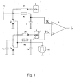
- FIG Fig. 1 A first embodiment of a circuit arrangement according to the invention is shown in FIG Fig. 1 shown.
- Electronic switches 2, 2a are periodically turned on by a square wave generator 10 at a control frequency 1 / (tone + Toff) for a time Ton and turned off for a time Toff.
- Ton a measuring capacitance or measuring electrode 1 and a fixed reference capacitance 1 a through the switches 2 and 2a with a fixed potential, in this case, for example, mass connected.
- a fixed potential in this case, for example, mass connected.
- the measuring capacity 1 and the reference capacity 1 a discharge abruptly.
- After this time sound open the switches 2 and 2a.
- the capacitances 1 and 1 a are charged via the respective associated resistors 3 and 3a.
- charging currents are supplied by a fixed DC voltage source U S 6, which can be realized for example by a stabilized internal sensor supply, and an adjustable DC voltage source U V 8.
- the charging voltages at the capacitors 1 and 1a respectively, increase according to an e-function, which is the charging function of a capacitor. The voltage increase is directly dependent on the size of the capacitors, the size of the charging resistors or charging currents and the supply voltages.
- the maximum charging voltage U Lend is not reached after the time interval Toff, before the capacitors are discharged abruptly again by closing the switches 2 and 2a during the time interval Ton. The loading and unloading continues in time with the generator 10.
- the signal curves are shown schematically in FIG Fig. 2 shown. From the periodic signal waveforms, which adjust at the capacitances in the form of the voltages U L1 , the charging voltage of the measuring capacitance, and U L2 , the charging voltage of the reference capacitance, the value of the measuring capacitance 1 is concluded in the manner described below. For this purpose, an averaging of the charging voltages U L1 and U L2 is the Measuring capacity 1 and the reference capacitance 1a provided. This averaging is realized by first-order RC low-pass filters formed by resistors 4 and 4a and capacitors 7 and 7a, respectively, which to some extent sift out the arithmetic mean value or the dc voltage component of the alternating signal.
- the resistors 4 and 4a should be for good decoupling from the charge and discharge preferably at least five times greater than the resistors 3 and 3a.
- the basic idea of the invention is this averaging of the charging and discharging curves at the two capacities: measuring capacity and reference capacity.
- the mean values or DC components of the charging voltages are in each case reversibly unambiguously assigned to the achieved charging end voltages, as in FIG Fig. 2 It can be seen where the charging voltage U L1 , an average value M 1 and the charging voltage U L2 are assigned an average value M 2 .
- These signals M 1 and M 2 are fed to a voltage comparator 9.
- the voltage at the "-" input is directly influenced by the measured variable. It decreases as the capacity 1 increases, which results in a decrease in the charge relaxation U Lend1 and thus in the mean value M 1 .
- the comparator 9 tilts from low to high State and outputs, for example, a signal S indicating, for example, the detection of a medium.
- a signal S indicating, for example, the detection of a medium.
- the adjustment of the sensitivity can be done in a wide range by the adjustable DC voltage U V by means of the adjustable voltage source 8.
- the reference circuit part which is constructed symmetrically to the measuring circuit part, so to speak counter to the measuring circuit part, is in FIG. 1 each marked with the reference numeral "a".
- the circuit arrangement Due to the symmetrical, ie the same design of the two circuit parts occur component drifts, e.g. Temperature drifts or drifts due to aging of components in both branches equal. The same drifting in both branches results in so far a theoretical differential voltage zero. As a result, drifting phenomena are largely eliminated. For this reason, the circuit arrangement has a very low temperature dependence and thus a very high sensitivity that can be achieved.
- the sensory quality of the circuit arrangement described above is essentially determined by the properties of the electronic switches 2 and in particular by their parasitic capacitances.
- the switches may e.g. be implemented cost-effectively with junction FETs or diode networks.
- the high immunity to interference is due to the fact that in a linear system many signals are superimposed undisturbed.
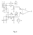
- FIG. 3 Another embodiment of the circuit arrangement will be described below in connection with Fig. 3 described, wherein like elements in Fig. 3 with the same reference numerals as in Fig. 1 are designated, so that with respect to the description of the above fully incorporated by reference.
- the circuit arrangement in Fig. 3 is different from the one in Fig. 2 in that the measuring electrode 1 is surrounded by an annular compensating electrode 11.
- This compensation electrode 11 The object of the invention is to minimize disturbances which are caused by capacitive influences, for example, of a plastic housing in which the circuit arrangement and the sensor are installed, on the measuring electrode 1.
- the compensation electrode 11 counteracts disturbing influences, for example external buildup of a medium on the sensor housing after immersion and extraction in the case of a filling level query by a compensating alternating field.
- This circuit arrangement is used in particular in free zone application.
- FIG. 4 illustrated embodiment differs from the in Fig. 1 represented in that the measuring electrode 1 is surrounded by a shield electrode 13.
- the shielding electrode 13 serves to shield the rear of the measuring electrode 1 and, to that extent, is arranged directly on the back of the measuring electrode or surrounds the measuring electrode on the back.
- the shield electrode 13 is buffered by a non-inverting amplifier 14 with the voltage gain factor 1 and the highest possible impedance input and low-impedance output.
- FIG Fig. 5 A further embodiment of a circuit according to the invention is shown in FIG Fig. 5 again, wherein here again the same elements with the same reference numerals as in Fig. 1 and Fig. 2 are provided so that with respect to their description to the above reference is made.
- the circuit arrangement in Fig. 5 is different from the ones in Fig. 1 to Fig. 4 represented by the fact that instead of the voltage source 6 and the resistor 3, a fixed DC power source 15 and instead of the voltage source 8 and the resistor 3a, an adjustable DC power source 16 are provided.
- the charging of the measuring capacitance 1 or the reference capacitance 1 a via these constant current sources 15 and 16 not according to an e-function, but temporally linear.
Landscapes
- Physics & Mathematics (AREA)
- General Physics & Mathematics (AREA)
- Engineering & Computer Science (AREA)
- Power Engineering (AREA)
- Electromagnetism (AREA)
- Thermal Sciences (AREA)
- Fluid Mechanics (AREA)
- Measurement Of Resistance Or Impedance (AREA)
Applications Claiming Priority (1)
| Application Number | Priority Date | Filing Date | Title |
|---|---|---|---|
| DE102009017011A DE102009017011A1 (de) | 2009-04-14 | 2009-04-14 | Schaltungsanordnung zur Bestimmung einer Messkapazität |
Publications (3)
| Publication Number | Publication Date |
|---|---|
| EP2241868A2 true EP2241868A2 (fr) | 2010-10-20 |
| EP2241868A3 EP2241868A3 (fr) | 2014-03-05 |
| EP2241868B1 EP2241868B1 (fr) | 2018-05-02 |
Family
ID=42411668
Family Applications (1)
| Application Number | Title | Priority Date | Filing Date |
|---|---|---|---|
| EP10003662.3A Active EP2241868B1 (fr) | 2009-04-14 | 2010-04-01 | Circuit destiné à la détermination d'une capacité de mesure |
Country Status (3)
| Country | Link |
|---|---|
| US (1) | US8587329B2 (fr) |
| EP (1) | EP2241868B1 (fr) |
| DE (1) | DE102009017011A1 (fr) |
Cited By (5)
| Publication number | Priority date | Publication date | Assignee | Title |
|---|---|---|---|---|
| EP2977717A1 (fr) * | 2014-07-25 | 2016-01-27 | Pepperl + Fuchs GmbH | Procédé et dispositif destinés à mesurer la hauteur d'empilement d'un support d'impression |
| EP2977716A1 (fr) * | 2014-07-25 | 2016-01-27 | Pepperl + Fuchs GmbH | Procédé et dispositif destinés à mesurer la hauteur d'empilement d'un support d'impression |
| WO2018127727A1 (fr) * | 2016-01-06 | 2018-07-12 | Disruptive Technologies Research As | Circuit de lecture de capteur capacitif |
| CN110998248A (zh) * | 2017-08-09 | 2020-04-10 | 代傲表计有限公司 | 用于确定关于流体和/或流体流的流体参量的测量设备 |
| US11073951B2 (en) | 2014-10-31 | 2021-07-27 | Semtech Corporation | Method and device for improved accuracy of proximity and touch detection in mobile devices |
Families Citing this family (19)
| Publication number | Priority date | Publication date | Assignee | Title |
|---|---|---|---|---|
| JP5332989B2 (ja) * | 2009-07-10 | 2013-11-06 | ソニー株式会社 | 液体タンクおよび燃料電池 |
| DE102010040434B4 (de) * | 2010-09-08 | 2020-01-30 | BSH Hausgeräte GmbH | Kapazitive Bedieneinrichtung für ein Haushaltsgerät, Haushaltsgerät und Verfahren zum Betreiben einer kapazitiven Bedieneinrichtung in einem Haushaltsgerät |
| US8760176B2 (en) * | 2010-11-10 | 2014-06-24 | St-Ericsson Sa | Methods and systems for production testing of DCO capacitors |
| DE102011013559B8 (de) * | 2011-03-10 | 2013-01-10 | iSEMcon GmbH | Schaltungs- oder Messanordnung zur kapazitiven, berührenden und/oder berührungslosen Überwachung eines Füllstandes und/oder einer Leckage leitfähiger Medien und Verfahren hierzu |
| KR20130007120A (ko) * | 2011-06-29 | 2013-01-18 | 에스케이하이닉스 주식회사 | 반도체 장치 및 그의 테스트 방법 |
| CN103513106A (zh) * | 2012-06-26 | 2014-01-15 | 中兴通讯股份有限公司 | 一种测量方法、测量电路及监控装置 |
| DE102012020925A1 (de) | 2012-10-25 | 2014-04-30 | Balluff Gmbh | Kapazitiver Sensor |
| DE102013005963B4 (de) | 2013-04-09 | 2026-04-16 | Balluff Gmbh | Kapazitiver Füllstandssensor |
| DE202014005969U1 (de) | 2014-07-25 | 2014-08-22 | Pepperl + Fuchs Gmbh | Vorrichtung zur Messung von Ladungsänderungszeiten |
| DE102014216247B4 (de) * | 2014-08-15 | 2019-06-13 | Mayser Gmbh & Co. Kg | Sensorsystem und Verfahren zur kapazitiven Erfassung von Hindernissen |
| DE102015208060A1 (de) * | 2015-02-12 | 2016-08-18 | Ifm Electronic Gmbh | Verfahren zum Betrieb eines Impulsgenerators für kapazitive Sensoren und Impulsgenerator |
| CN104730341A (zh) * | 2015-03-10 | 2015-06-24 | 昆山龙腾光电有限公司 | 阻抗检测电路、显示器检测装置及方法 |
| KR20170003041A (ko) | 2015-06-30 | 2017-01-09 | 삼성전자주식회사 | 유효한 유저 입력을 판단하는 전자 장치 |
| US10041981B2 (en) * | 2015-10-30 | 2018-08-07 | Silicon Laboratories Inc. | Capacitor sensing system |
| DE102017205908B4 (de) * | 2017-04-06 | 2019-04-04 | Marius Czardybon | Auswerteschaltung, System und Verfahren zum Auswerten eines kapazitiven oder induktiven Sensors |
| JP7605331B2 (ja) * | 2021-09-10 | 2024-12-24 | 株式会社村田製作所 | 静電容量センサ、及び、測定器 |
| EP4270789A1 (fr) * | 2022-04-27 | 2023-11-01 | NXP USA, Inc. | Capteur tactile capacitif |
| DE102022131053B3 (de) | 2022-11-23 | 2024-04-04 | Balluff Gmbh | Schaltungsanordnungen zur Messung wenigstens einer Kapazität |
| CN119535014B (zh) * | 2025-01-23 | 2025-05-30 | 杭州荷声科技有限公司 | 用于超声换能器阵列的自测试装置 |
Citations (7)
| Publication number | Priority date | Publication date | Assignee | Title |
|---|---|---|---|---|
| DE1673841A1 (de) | 1968-03-18 | 1971-06-24 | Schaller Werner Dipl Ing | Geraet zum Anzeigen des Vorhandenseins,der Annaeherung oder der Vergroesserung von festen Koerpern,Fluessigkeiten oder Gasen |
| DE19701899C2 (de) | 1996-01-21 | 2001-01-25 | Ifm Electronic Gmbh | Schaltungsanordnung und Verfahren zur Erfassung der Kapazität bzw. einer Kapazitätsänderung eines kapazitiven Schaltungs- oder Bauelementes |
| DE19945330A1 (de) | 1999-09-22 | 2001-04-26 | Sie Sensorik Ind Elektronik Gm | Verfahren zur Detektion und Auswertung kleiner Kapazitätsänderungen zur Umsetzung in ein Schaltsignal und kapazitiver Sensor hierzu |
| DE19949985A1 (de) | 1999-10-15 | 2001-05-10 | Sie Sensorik Ind Elektronik Gm | Kapazitiver Sensor zur Detektion des Füllstandes eines Mediums in einem Behälter |
| DE10156580A1 (de) | 2001-11-20 | 2003-05-28 | Sie Sensorik Ind Elektronik Gm | Oszillatorschaltungen zur Detektion kleiner Kapazitäten oder Kapazitätsunterschiede zum Einsatz in kapazitiven Sensoren |
| EP1093225B1 (fr) | 1999-10-15 | 2005-06-08 | i f m electronic gmbh | Commutateur de proximité |
| DE102005057558A1 (de) | 2005-11-30 | 2007-06-06 | Sie Sensorik Industrie-Elektronik Gmbh | Sensor zur berührungslosen Detektion des Füllstandes eines flüssigen und anhaltenden Mediums hoher Leitfähigkeit, insbesonere Blut, durch eine nichtmetallische Behälterwand eines Behälters und Verfahren hierzu |
Family Cites Families (21)
| Publication number | Priority date | Publication date | Assignee | Title |
|---|---|---|---|---|
| US3379972A (en) * | 1963-12-26 | 1968-04-23 | Reliance Electric & Eng Co | Non-contacting displacement gauge having a feedback means for controlling the vibration amplitude of the probe |
| US3458803A (en) * | 1966-03-21 | 1969-07-29 | David E Maguire | Apparatus and method for directly measuring capacitance and dissipation factor of capacitors |
| JPS539542B2 (fr) * | 1972-09-21 | 1978-04-06 | ||
| DE3143114A1 (de) * | 1980-11-07 | 1982-07-15 | Mestra AG, 4153 Reinach | Verfahren und schaltung zur messung von kapazitaeten |
| US4633168A (en) * | 1984-11-30 | 1986-12-30 | Borg-Warner Corporation | Measuring system for determining the reactance ratio of a pair of reactive devices |
| DE3544187A1 (de) * | 1985-12-13 | 1987-06-19 | Flowtec Ag | Kapazitaetsmessschaltung |
| US4831325A (en) * | 1987-04-01 | 1989-05-16 | General Signal Corporation | Capacitance measuring circuit |
| FR2660795B1 (fr) * | 1990-04-10 | 1994-01-07 | Sgs Thomson Microelectronics Sa | Circuit de detection de fusible. |
| DE4116961A1 (de) * | 1991-05-24 | 1992-11-26 | Abb Patent Gmbh | Messschaltung zur messung einer kapazitaet |
| US5294889A (en) * | 1992-03-27 | 1994-03-15 | Tandy Corporation | Battery operated capacitance measurement circuit |
| US6194903B1 (en) * | 1996-01-21 | 2001-02-27 | I F M Electronic Gmbh | Circuit for acquisition of the capacitance or capacitance change of a capacitive circuit element or component |
| DE19744152A1 (de) * | 1997-10-07 | 1999-04-29 | Ifm Electronic Gmbh | Schaltungsanordnung zur Erfassung der Kapazität bzw. einer Kapazitätsänderung eines kapazitiven Schaltungs- oder Bauelementes |
| TW464764B (en) * | 2000-06-14 | 2001-11-21 | Faraday Tech Corp | Measurement circuit of chip capacitance |
| US6828794B2 (en) * | 2002-10-24 | 2004-12-07 | Cambustion Limited | Electrostatic particle measurement |
| JP2004219311A (ja) * | 2003-01-16 | 2004-08-05 | Omron Corp | 静電容量センサ及び開閉体挟み込み検知装置 |
| US7312616B2 (en) * | 2006-01-20 | 2007-12-25 | Cypress Semiconductor Corporation | Successive approximate capacitance measurement circuit |
| PL1862806T3 (pl) * | 2006-06-01 | 2018-01-31 | Electrolux Home Products Corp Nv | Sposób i urządzenie do pomiaru pojemności elektrycznej elementu pojemnościowego |
| KR100919212B1 (ko) * | 2007-09-19 | 2009-09-28 | 주식회사 포인칩스 | 터치센서의 정전용량 측정회로 |
| TWI391678B (zh) * | 2009-09-30 | 2013-04-01 | Raydium Semiconductor Corp | 電容值測量電路與其方法 |
| TWI392877B (zh) * | 2009-11-17 | 2013-04-11 | Ili Technology Corp | 電容感測電路以及電容差異感測方法 |
| TWI447402B (zh) * | 2012-03-05 | 2014-08-01 | Mstar Semiconductor Inc | 電容偵測裝置及應用該電容偵測裝置之電容式觸控系統 |
-
2009
- 2009-04-14 DE DE102009017011A patent/DE102009017011A1/de not_active Withdrawn
-
2010
- 2010-04-01 EP EP10003662.3A patent/EP2241868B1/fr active Active
- 2010-04-13 US US12/798,887 patent/US8587329B2/en active Active
Patent Citations (7)
| Publication number | Priority date | Publication date | Assignee | Title |
|---|---|---|---|---|
| DE1673841A1 (de) | 1968-03-18 | 1971-06-24 | Schaller Werner Dipl Ing | Geraet zum Anzeigen des Vorhandenseins,der Annaeherung oder der Vergroesserung von festen Koerpern,Fluessigkeiten oder Gasen |
| DE19701899C2 (de) | 1996-01-21 | 2001-01-25 | Ifm Electronic Gmbh | Schaltungsanordnung und Verfahren zur Erfassung der Kapazität bzw. einer Kapazitätsänderung eines kapazitiven Schaltungs- oder Bauelementes |
| DE19945330A1 (de) | 1999-09-22 | 2001-04-26 | Sie Sensorik Ind Elektronik Gm | Verfahren zur Detektion und Auswertung kleiner Kapazitätsänderungen zur Umsetzung in ein Schaltsignal und kapazitiver Sensor hierzu |
| DE19949985A1 (de) | 1999-10-15 | 2001-05-10 | Sie Sensorik Ind Elektronik Gm | Kapazitiver Sensor zur Detektion des Füllstandes eines Mediums in einem Behälter |
| EP1093225B1 (fr) | 1999-10-15 | 2005-06-08 | i f m electronic gmbh | Commutateur de proximité |
| DE10156580A1 (de) | 2001-11-20 | 2003-05-28 | Sie Sensorik Ind Elektronik Gm | Oszillatorschaltungen zur Detektion kleiner Kapazitäten oder Kapazitätsunterschiede zum Einsatz in kapazitiven Sensoren |
| DE102005057558A1 (de) | 2005-11-30 | 2007-06-06 | Sie Sensorik Industrie-Elektronik Gmbh | Sensor zur berührungslosen Detektion des Füllstandes eines flüssigen und anhaltenden Mediums hoher Leitfähigkeit, insbesonere Blut, durch eine nichtmetallische Behälterwand eines Behälters und Verfahren hierzu |
Cited By (10)
| Publication number | Priority date | Publication date | Assignee | Title |
|---|---|---|---|---|
| EP2977717A1 (fr) * | 2014-07-25 | 2016-01-27 | Pepperl + Fuchs GmbH | Procédé et dispositif destinés à mesurer la hauteur d'empilement d'un support d'impression |
| EP2977716A1 (fr) * | 2014-07-25 | 2016-01-27 | Pepperl + Fuchs GmbH | Procédé et dispositif destinés à mesurer la hauteur d'empilement d'un support d'impression |
| US11073951B2 (en) | 2014-10-31 | 2021-07-27 | Semtech Corporation | Method and device for improved accuracy of proximity and touch detection in mobile devices |
| US11112917B2 (en) | 2014-10-31 | 2021-09-07 | Semtech Corporation | Method and device for improved accuracy of proximity and touch detection in mobile devices |
| EP3694107B1 (fr) * | 2014-10-31 | 2022-10-12 | Semtech Corporation | Procédé et dispositif permettant d'améliorer la précision de détection de toucher et de proximité dans des dispositifs mobiles |
| US11474648B2 (en) | 2014-10-31 | 2022-10-18 | Semtech Corporation | Method and device for improved accuracy of proximity and touch detection in mobile devices |
| US12299243B2 (en) | 2014-10-31 | 2025-05-13 | Semtech Corporation | Method and device for improved accuracy of proximity and touch detection in mobile devices |
| WO2018127727A1 (fr) * | 2016-01-06 | 2018-07-12 | Disruptive Technologies Research As | Circuit de lecture de capteur capacitif |
| CN110998248A (zh) * | 2017-08-09 | 2020-04-10 | 代傲表计有限公司 | 用于确定关于流体和/或流体流的流体参量的测量设备 |
| CN110998248B (zh) * | 2017-08-09 | 2022-05-03 | 代傲表计有限公司 | 用于确定关于流体和/或流体流的流体参量的测量设备 |
Also Published As
| Publication number | Publication date |
|---|---|
| US8587329B2 (en) | 2013-11-19 |
| EP2241868B1 (fr) | 2018-05-02 |
| DE102009017011A1 (de) | 2010-10-28 |
| US20100259284A1 (en) | 2010-10-14 |
| EP2241868A3 (fr) | 2014-03-05 |
Similar Documents
| Publication | Publication Date | Title |
|---|---|---|
| EP2241868B1 (fr) | Circuit destiné à la détermination d'une capacité de mesure | |
| DE19701899C2 (de) | Schaltungsanordnung und Verfahren zur Erfassung der Kapazität bzw. einer Kapazitätsänderung eines kapazitiven Schaltungs- oder Bauelementes | |
| EP1500940B1 (fr) | Procédé pour évaluer un condensateur | |
| EP3152530B1 (fr) | Procédé et dispositif de surveillance du niveau d'un milieu dans un récipient | |
| DE19520049C2 (de) | Sensorelement vom Kapazitätstyp | |
| DE102010039272B3 (de) | Kapazitätsmessschaltung, Sensorsystem und Verfahren zum Messen einer Kapazität unter Verwendung eines sinusförmigen Spannungssignals | |
| DE69515459T2 (de) | Kapazitiver Sensor | |
| DE102007047887A1 (de) | Kapazitätserfassungsvorrichtung | |
| DE102013005963A1 (de) | Kapazitiver Füllstandssensor | |
| DE102005028507B3 (de) | Verfahren zur Kapazitäts-Spannungs-Wandlung und Kapazitäts-Spannungs-Wandler | |
| EP1959570A2 (fr) | Détecteur d'approximation inductif | |
| DE60102976T2 (de) | Signalverarbeitung für einen piezoelektrischen Sensor mit Differenzierer und Integrierer | |
| DE102008027921B4 (de) | Admittanzmeßvorrichtung für einen Füllstandsensor | |
| EP3457369B1 (fr) | Circuit pour capteur de fumée | |
| DE10063557B4 (de) | Verfahren und Vorrichtung zum Messen von Pegelständen | |
| EP4483146A1 (fr) | Détermination de conductivité compensée | |
| DE102009002674A1 (de) | Admittanzmeßvorrichtung zur Überwachung eines Mediums | |
| DE102007025947B4 (de) | Integrierter kapazitiver Sensor | |
| EP0185255B1 (fr) | Procédé pour déterminer la polarité de composants électroniques et dispositif mettant en oeuvre ce procédé | |
| DE9421121U1 (de) | Vorrichtung zur Bestimmung einer jeweiligen örtlichen Position eines Körpers durch kapazitive Abtastung | |
| DE4001274C2 (fr) | ||
| DE3134322C2 (fr) | ||
| DE4435877C2 (de) | Kapazitiver Sensor | |
| EP4513199B1 (fr) | Commutateur de proximité pour la mesure de la vitesse d'un objet à mesurer | |
| DE102022131053B3 (de) | Schaltungsanordnungen zur Messung wenigstens einer Kapazität |
Legal Events
| Date | Code | Title | Description |
|---|---|---|---|
| PUAI | Public reference made under article 153(3) epc to a published international application that has entered the european phase |
Free format text: ORIGINAL CODE: 0009012 |
|
| AK | Designated contracting states |
Kind code of ref document: A2 Designated state(s): AT BE BG CH CY CZ DE DK EE ES FI FR GB GR HR HU IE IS IT LI LT LU LV MC MK MT NL NO PL PT RO SE SI SK SM TR |
|
| AX | Request for extension of the european patent |
Extension state: AL BA ME RS |
|
| PUAL | Search report despatched |
Free format text: ORIGINAL CODE: 0009013 |
|
| AK | Designated contracting states |
Kind code of ref document: A3 Designated state(s): AT BE BG CH CY CZ DE DK EE ES FI FR GB GR HR HU IE IS IT LI LT LU LV MC MK MT NL NO PL PT RO SE SI SK SM TR |
|
| AX | Request for extension of the european patent |
Extension state: AL BA ME RS |
|
| RIC1 | Information provided on ipc code assigned before grant |
Ipc: G01D 5/24 20060101ALI20140129BHEP Ipc: G01R 27/26 20060101ALI20140129BHEP Ipc: G01F 23/26 20060101AFI20140129BHEP |
|
| 17P | Request for examination filed |
Effective date: 20140514 |
|
| RBV | Designated contracting states (corrected) |
Designated state(s): AT BE BG CH CY CZ DE DK EE ES FI FR GB GR HR HU IE IS IT LI LT LU LV MC MK MT NL NO PL PT RO SE SI SK SM TR |
|
| GRAP | Despatch of communication of intention to grant a patent |
Free format text: ORIGINAL CODE: EPIDOSNIGR1 |
|
| STAA | Information on the status of an ep patent application or granted ep patent |
Free format text: STATUS: GRANT OF PATENT IS INTENDED |
|
| INTG | Intention to grant announced |
Effective date: 20171113 |
|
| GRAS | Grant fee paid |
Free format text: ORIGINAL CODE: EPIDOSNIGR3 |
|
| GRAJ | Information related to disapproval of communication of intention to grant by the applicant or resumption of examination proceedings by the epo deleted |
Free format text: ORIGINAL CODE: EPIDOSDIGR1 |
|
| GRAL | Information related to payment of fee for publishing/printing deleted |
Free format text: ORIGINAL CODE: EPIDOSDIGR3 |
|
| STAA | Information on the status of an ep patent application or granted ep patent |
Free format text: STATUS: REQUEST FOR EXAMINATION WAS MADE |
|
| INTC | Intention to grant announced (deleted) | ||
| GRAJ | Information related to disapproval of communication of intention to grant by the applicant or resumption of examination proceedings by the epo deleted |
Free format text: ORIGINAL CODE: EPIDOSDIGR1 |
|
| GRAP | Despatch of communication of intention to grant a patent |
Free format text: ORIGINAL CODE: EPIDOSNIGR1 |
|
| GRAR | Information related to intention to grant a patent recorded |
Free format text: ORIGINAL CODE: EPIDOSNIGR71 |
|
| STAA | Information on the status of an ep patent application or granted ep patent |
Free format text: STATUS: GRANT OF PATENT IS INTENDED |
|
| GRAA | (expected) grant |
Free format text: ORIGINAL CODE: 0009210 |
|
| STAA | Information on the status of an ep patent application or granted ep patent |
Free format text: STATUS: THE PATENT HAS BEEN GRANTED |
|
| INTG | Intention to grant announced |
Effective date: 20180314 |
|
| AK | Designated contracting states |
Kind code of ref document: B1 Designated state(s): AT BE BG CH CY CZ DE DK EE ES FI FR GB GR HR HU IE IS IT LI LT LU LV MC MK MT NL NO PL PT RO SE SI SK SM TR |
|
| REG | Reference to a national code |
Ref country code: GB Ref legal event code: FG4D Free format text: NOT ENGLISH |
|
| REG | Reference to a national code |
Ref country code: CH Ref legal event code: EP Ref country code: AT Ref legal event code: REF Ref document number: 995779 Country of ref document: AT Kind code of ref document: T Effective date: 20180515 |
|
| REG | Reference to a national code |
Ref country code: DE Ref legal event code: R096 Ref document number: 502010014930 Country of ref document: DE |
|
| REG | Reference to a national code |
Ref country code: IE Ref legal event code: FG4D Free format text: LANGUAGE OF EP DOCUMENT: GERMAN |
|
| REG | Reference to a national code |
Ref country code: CH Ref legal event code: NV Representative=s name: RENTSCH PARTNER AG, CH |
|
| REG | Reference to a national code |
Ref country code: NL Ref legal event code: MP Effective date: 20180502 |
|
| REG | Reference to a national code |
Ref country code: LT Ref legal event code: MG4D |
|
| PG25 | Lapsed in a contracting state [announced via postgrant information from national office to epo] |
Ref country code: LT Free format text: LAPSE BECAUSE OF FAILURE TO SUBMIT A TRANSLATION OF THE DESCRIPTION OR TO PAY THE FEE WITHIN THE PRESCRIBED TIME-LIMIT Effective date: 20180502 Ref country code: SE Free format text: LAPSE BECAUSE OF FAILURE TO SUBMIT A TRANSLATION OF THE DESCRIPTION OR TO PAY THE FEE WITHIN THE PRESCRIBED TIME-LIMIT Effective date: 20180502 Ref country code: FI Free format text: LAPSE BECAUSE OF FAILURE TO SUBMIT A TRANSLATION OF THE DESCRIPTION OR TO PAY THE FEE WITHIN THE PRESCRIBED TIME-LIMIT Effective date: 20180502 Ref country code: ES Free format text: LAPSE BECAUSE OF FAILURE TO SUBMIT A TRANSLATION OF THE DESCRIPTION OR TO PAY THE FEE WITHIN THE PRESCRIBED TIME-LIMIT Effective date: 20180502 Ref country code: NO Free format text: LAPSE BECAUSE OF FAILURE TO SUBMIT A TRANSLATION OF THE DESCRIPTION OR TO PAY THE FEE WITHIN THE PRESCRIBED TIME-LIMIT Effective date: 20180802 Ref country code: BG Free format text: LAPSE BECAUSE OF FAILURE TO SUBMIT A TRANSLATION OF THE DESCRIPTION OR TO PAY THE FEE WITHIN THE PRESCRIBED TIME-LIMIT Effective date: 20180802 |
|
| PG25 | Lapsed in a contracting state [announced via postgrant information from national office to epo] |
Ref country code: NL Free format text: LAPSE BECAUSE OF FAILURE TO SUBMIT A TRANSLATION OF THE DESCRIPTION OR TO PAY THE FEE WITHIN THE PRESCRIBED TIME-LIMIT Effective date: 20180502 Ref country code: LV Free format text: LAPSE BECAUSE OF FAILURE TO SUBMIT A TRANSLATION OF THE DESCRIPTION OR TO PAY THE FEE WITHIN THE PRESCRIBED TIME-LIMIT Effective date: 20180502 Ref country code: HR Free format text: LAPSE BECAUSE OF FAILURE TO SUBMIT A TRANSLATION OF THE DESCRIPTION OR TO PAY THE FEE WITHIN THE PRESCRIBED TIME-LIMIT Effective date: 20180502 Ref country code: GR Free format text: LAPSE BECAUSE OF FAILURE TO SUBMIT A TRANSLATION OF THE DESCRIPTION OR TO PAY THE FEE WITHIN THE PRESCRIBED TIME-LIMIT Effective date: 20180803 |
|
| PG25 | Lapsed in a contracting state [announced via postgrant information from national office to epo] |
Ref country code: PT Free format text: LAPSE BECAUSE OF FAILURE TO SUBMIT A TRANSLATION OF THE DESCRIPTION OR TO PAY THE FEE WITHIN THE PRESCRIBED TIME-LIMIT Effective date: 20180903 |
|
| PG25 | Lapsed in a contracting state [announced via postgrant information from national office to epo] |
Ref country code: EE Free format text: LAPSE BECAUSE OF FAILURE TO SUBMIT A TRANSLATION OF THE DESCRIPTION OR TO PAY THE FEE WITHIN THE PRESCRIBED TIME-LIMIT Effective date: 20180502 Ref country code: DK Free format text: LAPSE BECAUSE OF FAILURE TO SUBMIT A TRANSLATION OF THE DESCRIPTION OR TO PAY THE FEE WITHIN THE PRESCRIBED TIME-LIMIT Effective date: 20180502 Ref country code: SK Free format text: LAPSE BECAUSE OF FAILURE TO SUBMIT A TRANSLATION OF THE DESCRIPTION OR TO PAY THE FEE WITHIN THE PRESCRIBED TIME-LIMIT Effective date: 20180502 Ref country code: RO Free format text: LAPSE BECAUSE OF FAILURE TO SUBMIT A TRANSLATION OF THE DESCRIPTION OR TO PAY THE FEE WITHIN THE PRESCRIBED TIME-LIMIT Effective date: 20180502 Ref country code: PL Free format text: LAPSE BECAUSE OF FAILURE TO SUBMIT A TRANSLATION OF THE DESCRIPTION OR TO PAY THE FEE WITHIN THE PRESCRIBED TIME-LIMIT Effective date: 20180502 Ref country code: CZ Free format text: LAPSE BECAUSE OF FAILURE TO SUBMIT A TRANSLATION OF THE DESCRIPTION OR TO PAY THE FEE WITHIN THE PRESCRIBED TIME-LIMIT Effective date: 20180502 |
|
| REG | Reference to a national code |
Ref country code: DE Ref legal event code: R097 Ref document number: 502010014930 Country of ref document: DE |
|
| PG25 | Lapsed in a contracting state [announced via postgrant information from national office to epo] |
Ref country code: IT Free format text: LAPSE BECAUSE OF FAILURE TO SUBMIT A TRANSLATION OF THE DESCRIPTION OR TO PAY THE FEE WITHIN THE PRESCRIBED TIME-LIMIT Effective date: 20180502 Ref country code: SM Free format text: LAPSE BECAUSE OF FAILURE TO SUBMIT A TRANSLATION OF THE DESCRIPTION OR TO PAY THE FEE WITHIN THE PRESCRIBED TIME-LIMIT Effective date: 20180502 |
|
| PLBE | No opposition filed within time limit |
Free format text: ORIGINAL CODE: 0009261 |
|
| STAA | Information on the status of an ep patent application or granted ep patent |
Free format text: STATUS: NO OPPOSITION FILED WITHIN TIME LIMIT |
|
| 26N | No opposition filed |
Effective date: 20190205 |
|
| PG25 | Lapsed in a contracting state [announced via postgrant information from national office to epo] |
Ref country code: SI Free format text: LAPSE BECAUSE OF FAILURE TO SUBMIT A TRANSLATION OF THE DESCRIPTION OR TO PAY THE FEE WITHIN THE PRESCRIBED TIME-LIMIT Effective date: 20180502 |
|
| REG | Reference to a national code |
Ref country code: CH Ref legal event code: PL |
|
| REG | Reference to a national code |
Ref country code: BE Ref legal event code: MM Effective date: 20190430 |
|
| GBPC | Gb: european patent ceased through non-payment of renewal fee |
Effective date: 20190401 |
|
| PG25 | Lapsed in a contracting state [announced via postgrant information from national office to epo] |
Ref country code: MC Free format text: LAPSE BECAUSE OF FAILURE TO SUBMIT A TRANSLATION OF THE DESCRIPTION OR TO PAY THE FEE WITHIN THE PRESCRIBED TIME-LIMIT Effective date: 20180502 Ref country code: LU Free format text: LAPSE BECAUSE OF NON-PAYMENT OF DUE FEES Effective date: 20190401 |
|
| PG25 | Lapsed in a contracting state [announced via postgrant information from national office to epo] |
Ref country code: GB Free format text: LAPSE BECAUSE OF NON-PAYMENT OF DUE FEES Effective date: 20190401 Ref country code: LI Free format text: LAPSE BECAUSE OF NON-PAYMENT OF DUE FEES Effective date: 20190430 Ref country code: CH Free format text: LAPSE BECAUSE OF NON-PAYMENT OF DUE FEES Effective date: 20190430 |
|
| PG25 | Lapsed in a contracting state [announced via postgrant information from national office to epo] |
Ref country code: FR Free format text: LAPSE BECAUSE OF NON-PAYMENT OF DUE FEES Effective date: 20190430 Ref country code: BE Free format text: LAPSE BECAUSE OF NON-PAYMENT OF DUE FEES Effective date: 20190430 |
|
| PG25 | Lapsed in a contracting state [announced via postgrant information from national office to epo] |
Ref country code: TR Free format text: LAPSE BECAUSE OF FAILURE TO SUBMIT A TRANSLATION OF THE DESCRIPTION OR TO PAY THE FEE WITHIN THE PRESCRIBED TIME-LIMIT Effective date: 20180502 |
|
| PG25 | Lapsed in a contracting state [announced via postgrant information from national office to epo] |
Ref country code: IE Free format text: LAPSE BECAUSE OF NON-PAYMENT OF DUE FEES Effective date: 20190401 |
|
| REG | Reference to a national code |
Ref country code: AT Ref legal event code: MM01 Ref document number: 995779 Country of ref document: AT Kind code of ref document: T Effective date: 20190401 |
|
| PG25 | Lapsed in a contracting state [announced via postgrant information from national office to epo] |
Ref country code: AT Free format text: LAPSE BECAUSE OF NON-PAYMENT OF DUE FEES Effective date: 20190401 |
|
| PG25 | Lapsed in a contracting state [announced via postgrant information from national office to epo] |
Ref country code: CY Free format text: LAPSE BECAUSE OF FAILURE TO SUBMIT A TRANSLATION OF THE DESCRIPTION OR TO PAY THE FEE WITHIN THE PRESCRIBED TIME-LIMIT Effective date: 20180502 |
|
| PG25 | Lapsed in a contracting state [announced via postgrant information from national office to epo] |
Ref country code: IS Free format text: LAPSE BECAUSE OF FAILURE TO SUBMIT A TRANSLATION OF THE DESCRIPTION OR TO PAY THE FEE WITHIN THE PRESCRIBED TIME-LIMIT Effective date: 20180902 |
|
| PG25 | Lapsed in a contracting state [announced via postgrant information from national office to epo] |
Ref country code: MT Free format text: LAPSE BECAUSE OF FAILURE TO SUBMIT A TRANSLATION OF THE DESCRIPTION OR TO PAY THE FEE WITHIN THE PRESCRIBED TIME-LIMIT Effective date: 20180502 Ref country code: HU Free format text: LAPSE BECAUSE OF FAILURE TO SUBMIT A TRANSLATION OF THE DESCRIPTION OR TO PAY THE FEE WITHIN THE PRESCRIBED TIME-LIMIT; INVALID AB INITIO Effective date: 20100401 |
|
| PG25 | Lapsed in a contracting state [announced via postgrant information from national office to epo] |
Ref country code: MK Free format text: LAPSE BECAUSE OF FAILURE TO SUBMIT A TRANSLATION OF THE DESCRIPTION OR TO PAY THE FEE WITHIN THE PRESCRIBED TIME-LIMIT Effective date: 20180502 |
|
| P01 | Opt-out of the competence of the unified patent court (upc) registered |
Effective date: 20230530 |
|
| PGFP | Annual fee paid to national office [announced via postgrant information from national office to epo] |
Ref country code: DE Payment date: 20250318 Year of fee payment: 16 |