EP2241909A2 - Nanostrukturierte Antireflexionsbeschichtungen und zugehörige Verfahren und Vorrichtungen - Google Patents
Nanostrukturierte Antireflexionsbeschichtungen und zugehörige Verfahren und Vorrichtungen Download PDFInfo
- Publication number
- EP2241909A2 EP2241909A2 EP10157871A EP10157871A EP2241909A2 EP 2241909 A2 EP2241909 A2 EP 2241909A2 EP 10157871 A EP10157871 A EP 10157871A EP 10157871 A EP10157871 A EP 10157871A EP 2241909 A2 EP2241909 A2 EP 2241909A2
- Authority
- EP
- European Patent Office
- Prior art keywords
- nanostructures
- substrate
- reflection coating
- primary axis
- array
- Prior art date
- Legal status (The legal status is an assumption and is not a legal conclusion. Google has not performed a legal analysis and makes no representation as to the accuracy of the status listed.)
- Withdrawn
Links
- 238000000576 coating method Methods 0.000 title claims abstract description 103
- 238000000034 method Methods 0.000 title claims abstract description 41
- 239000002086 nanomaterial Substances 0.000 claims abstract description 174
- 239000000758 substrate Substances 0.000 claims abstract description 98
- 239000011248 coating agent Substances 0.000 claims abstract description 89
- 238000000151 deposition Methods 0.000 claims description 27
- 230000005693 optoelectronics Effects 0.000 claims description 27
- 239000000203 mixture Substances 0.000 claims description 22
- 230000008021 deposition Effects 0.000 claims description 21
- 239000004020 conductor Substances 0.000 claims description 18
- 238000001312 dry etching Methods 0.000 claims description 11
- 238000001039 wet etching Methods 0.000 claims description 10
- 230000005670 electromagnetic radiation Effects 0.000 claims description 9
- 239000002178 crystalline material Substances 0.000 claims description 8
- VYPSYNLAJGMNEJ-UHFFFAOYSA-N Silicium dioxide Chemical compound O=[Si]=O VYPSYNLAJGMNEJ-UHFFFAOYSA-N 0.000 description 20
- 239000000463 material Substances 0.000 description 19
- 210000004027 cell Anatomy 0.000 description 18
- 239000011521 glass Substances 0.000 description 16
- XLOMVQKBTHCTTD-UHFFFAOYSA-N Zinc monoxide Chemical compound [Zn]=O XLOMVQKBTHCTTD-UHFFFAOYSA-N 0.000 description 12
- GWEVSGVZZGPLCZ-UHFFFAOYSA-N Titan oxide Chemical compound O=[Ti]=O GWEVSGVZZGPLCZ-UHFFFAOYSA-N 0.000 description 10
- 239000002070 nanowire Substances 0.000 description 10
- 239000002073 nanorod Substances 0.000 description 8
- 230000008569 process Effects 0.000 description 8
- XOLBLPGZBRYERU-UHFFFAOYSA-N tin dioxide Chemical compound O=[Sn]=O XOLBLPGZBRYERU-UHFFFAOYSA-N 0.000 description 8
- 229910001887 tin oxide Inorganic materials 0.000 description 8
- 239000010408 film Substances 0.000 description 7
- 230000003287 optical effect Effects 0.000 description 7
- 239000000377 silicon dioxide Substances 0.000 description 7
- 230000007423 decrease Effects 0.000 description 6
- 229910052751 metal Inorganic materials 0.000 description 6
- 239000002184 metal Substances 0.000 description 6
- 238000001020 plasma etching Methods 0.000 description 6
- 239000010409 thin film Substances 0.000 description 6
- 239000011787 zinc oxide Substances 0.000 description 6
- 238000005229 chemical vapour deposition Methods 0.000 description 5
- 230000000694 effects Effects 0.000 description 5
- 239000010410 layer Substances 0.000 description 5
- -1 nanodots Substances 0.000 description 5
- 239000002077 nanosphere Substances 0.000 description 5
- 238000000054 nanosphere lithography Methods 0.000 description 5
- XEEYBQQBJWHFJM-UHFFFAOYSA-N Iron Chemical compound [Fe] XEEYBQQBJWHFJM-UHFFFAOYSA-N 0.000 description 4
- XUIMIQQOPSSXEZ-UHFFFAOYSA-N Silicon Chemical compound [Si] XUIMIQQOPSSXEZ-UHFFFAOYSA-N 0.000 description 4
- 229910020923 Sn-O Inorganic materials 0.000 description 4
- UCKMPCXJQFINFW-UHFFFAOYSA-N Sulphide Chemical compound [S-2] UCKMPCXJQFINFW-UHFFFAOYSA-N 0.000 description 4
- 238000010521 absorption reaction Methods 0.000 description 4
- 238000003491 array Methods 0.000 description 4
- 230000008859 change Effects 0.000 description 4
- 229910052681 coesite Inorganic materials 0.000 description 4
- 229910052906 cristobalite Inorganic materials 0.000 description 4
- 229910052738 indium Inorganic materials 0.000 description 4
- APFVFJFRJDLVQX-UHFFFAOYSA-N indium atom Chemical compound [In] APFVFJFRJDLVQX-UHFFFAOYSA-N 0.000 description 4
- 239000002105 nanoparticle Substances 0.000 description 4
- 239000002245 particle Substances 0.000 description 4
- 238000005240 physical vapour deposition Methods 0.000 description 4
- 230000005855 radiation Effects 0.000 description 4
- 229910052710 silicon Inorganic materials 0.000 description 4
- 239000010703 silicon Substances 0.000 description 4
- 229910052682 stishovite Inorganic materials 0.000 description 4
- XSOKHXFFCGXDJZ-UHFFFAOYSA-N telluride(2-) Chemical compound [Te-2] XSOKHXFFCGXDJZ-UHFFFAOYSA-N 0.000 description 4
- 229910052905 tridymite Inorganic materials 0.000 description 4
- 230000005540 biological transmission Effects 0.000 description 3
- 229910052760 oxygen Inorganic materials 0.000 description 3
- 230000000737 periodic effect Effects 0.000 description 3
- 238000002310 reflectometry Methods 0.000 description 3
- 239000004065 semiconductor Substances 0.000 description 3
- 229910052814 silicon oxide Inorganic materials 0.000 description 3
- SQGYOTSLMSWVJD-UHFFFAOYSA-N silver(1+) nitrate Chemical compound [Ag+].[O-]N(=O)=O SQGYOTSLMSWVJD-UHFFFAOYSA-N 0.000 description 3
- 239000005361 soda-lime glass Substances 0.000 description 3
- 239000007787 solid Substances 0.000 description 3
- 230000003595 spectral effect Effects 0.000 description 3
- WUPHOULIZUERAE-UHFFFAOYSA-N 3-(oxolan-2-yl)propanoic acid Chemical compound OC(=O)CCC1CCCO1 WUPHOULIZUERAE-UHFFFAOYSA-N 0.000 description 2
- CSCPPACGZOOCGX-UHFFFAOYSA-N Acetone Chemical compound CC(C)=O CSCPPACGZOOCGX-UHFFFAOYSA-N 0.000 description 2
- 229910017612 Cu(In,Ga)Se2 Inorganic materials 0.000 description 2
- GPXJNWSHGFTCBW-UHFFFAOYSA-N Indium phosphide Chemical compound [In]#P GPXJNWSHGFTCBW-UHFFFAOYSA-N 0.000 description 2
- 229910007611 Zn—In—O Inorganic materials 0.000 description 2
- 229910052782 aluminium Inorganic materials 0.000 description 2
- XAGFODPZIPBFFR-UHFFFAOYSA-N aluminium Chemical compound [Al] XAGFODPZIPBFFR-UHFFFAOYSA-N 0.000 description 2
- 239000005354 aluminosilicate glass Substances 0.000 description 2
- 229910021417 amorphous silicon Inorganic materials 0.000 description 2
- 238000000137 annealing Methods 0.000 description 2
- 230000015572 biosynthetic process Effects 0.000 description 2
- 239000005388 borosilicate glass Substances 0.000 description 2
- 229910052793 cadmium Inorganic materials 0.000 description 2
- 229910052980 cadmium sulfide Inorganic materials 0.000 description 2
- 238000000224 chemical solution deposition Methods 0.000 description 2
- 230000001427 coherent effect Effects 0.000 description 2
- 230000002301 combined effect Effects 0.000 description 2
- 239000002131 composite material Substances 0.000 description 2
- 229910021419 crystalline silicon Inorganic materials 0.000 description 2
- 239000003989 dielectric material Substances 0.000 description 2
- 238000003618 dip coating Methods 0.000 description 2
- 238000005530 etching Methods 0.000 description 2
- AMGQUBHHOARCQH-UHFFFAOYSA-N indium;oxotin Chemical compound [In].[Sn]=O AMGQUBHHOARCQH-UHFFFAOYSA-N 0.000 description 2
- 229910052742 iron Inorganic materials 0.000 description 2
- 230000001788 irregular Effects 0.000 description 2
- 238000005304 joining Methods 0.000 description 2
- 230000007246 mechanism Effects 0.000 description 2
- 238000012986 modification Methods 0.000 description 2
- 230000004048 modification Effects 0.000 description 2
- 239000002159 nanocrystal Substances 0.000 description 2
- 239000002071 nanotube Substances 0.000 description 2
- 239000002243 precursor Substances 0.000 description 2
- 238000011160 research Methods 0.000 description 2
- 239000002356 single layer Substances 0.000 description 2
- 238000004528 spin coating Methods 0.000 description 2
- 238000004544 sputter deposition Methods 0.000 description 2
- 229940071182 stannate Drugs 0.000 description 2
- 239000000126 substance Substances 0.000 description 2
- GKCNVZWZCYIBPR-UHFFFAOYSA-N sulfanylideneindium Chemical compound [In]=S GKCNVZWZCYIBPR-UHFFFAOYSA-N 0.000 description 2
- 150000004763 sulfides Chemical class 0.000 description 2
- 239000000725 suspension Substances 0.000 description 2
- 239000004408 titanium dioxide Substances 0.000 description 2
- 239000012780 transparent material Substances 0.000 description 2
- BNEMLSQAJOPTGK-UHFFFAOYSA-N zinc;dioxido(oxo)tin Chemical compound [Zn+2].[O-][Sn]([O-])=O BNEMLSQAJOPTGK-UHFFFAOYSA-N 0.000 description 2
- 229910004613 CdTe Inorganic materials 0.000 description 1
- 229910005540 GaP Inorganic materials 0.000 description 1
- 229910001218 Gallium arsenide Inorganic materials 0.000 description 1
- UFHFLCQGNIYNRP-UHFFFAOYSA-N Hydrogen Chemical compound [H][H] UFHFLCQGNIYNRP-UHFFFAOYSA-N 0.000 description 1
- 239000004793 Polystyrene Substances 0.000 description 1
- BLRPTPMANUNPDV-UHFFFAOYSA-N Silane Chemical compound [SiH4] BLRPTPMANUNPDV-UHFFFAOYSA-N 0.000 description 1
- 230000003667 anti-reflective effect Effects 0.000 description 1
- 238000000149 argon plasma sintering Methods 0.000 description 1
- QVGXLLKOCUKJST-UHFFFAOYSA-N atomic oxygen Chemical compound [O] QVGXLLKOCUKJST-UHFFFAOYSA-N 0.000 description 1
- 238000004140 cleaning Methods 0.000 description 1
- 239000000470 constituent Substances 0.000 description 1
- 239000013078 crystal Substances 0.000 description 1
- 230000003247 decreasing effect Effects 0.000 description 1
- 210000001787 dendrite Anatomy 0.000 description 1
- 238000007598 dipping method Methods 0.000 description 1
- 238000010894 electron beam technology Methods 0.000 description 1
- 230000008030 elimination Effects 0.000 description 1
- 238000003379 elimination reaction Methods 0.000 description 1
- 238000001704 evaporation Methods 0.000 description 1
- 230000008020 evaporation Effects 0.000 description 1
- 230000004907 flux Effects 0.000 description 1
- 230000006870 function Effects 0.000 description 1
- 239000005350 fused silica glass Substances 0.000 description 1
- HZXMRANICFIONG-UHFFFAOYSA-N gallium phosphide Chemical compound [Ga]#P HZXMRANICFIONG-UHFFFAOYSA-N 0.000 description 1
- 238000011065 in-situ storage Methods 0.000 description 1
- 238000007373 indentation Methods 0.000 description 1
- 238000009616 inductively coupled plasma Methods 0.000 description 1
- 239000007791 liquid phase Substances 0.000 description 1
- 238000004518 low pressure chemical vapour deposition Methods 0.000 description 1
- 238000004519 manufacturing process Methods 0.000 description 1
- 238000005259 measurement Methods 0.000 description 1
- 239000001301 oxygen Substances 0.000 description 1
- 238000000059 patterning Methods 0.000 description 1
- 239000012071 phase Substances 0.000 description 1
- 238000000623 plasma-assisted chemical vapour deposition Methods 0.000 description 1
- 229920000642 polymer Polymers 0.000 description 1
- 229920002223 polystyrene Polymers 0.000 description 1
- 238000001556 precipitation Methods 0.000 description 1
- 238000012545 processing Methods 0.000 description 1
- 239000010453 quartz Substances 0.000 description 1
- 230000009467 reduction Effects 0.000 description 1
- 229910000077 silane Inorganic materials 0.000 description 1
- 238000002791 soaking Methods 0.000 description 1
- 238000003980 solgel method Methods 0.000 description 1
- 238000001228 spectrum Methods 0.000 description 1
- 239000012798 spherical particle Substances 0.000 description 1
- 238000003786 synthesis reaction Methods 0.000 description 1
- 230000008685 targeting Effects 0.000 description 1
- 239000010936 titanium Substances 0.000 description 1
Images


Classifications
-
- G—PHYSICS
- G02—OPTICS
- G02B—OPTICAL ELEMENTS, SYSTEMS OR APPARATUS
- G02B1/00—Optical elements characterised by the material of which they are made; Optical coatings for optical elements
- G02B1/10—Optical coatings produced by application to, or surface treatment of, optical elements
- G02B1/11—Anti-reflection coatings
- G02B1/118—Anti-reflection coatings having sub-optical wavelength surface structures designed to provide an enhanced transmittance, e.g. moth-eye structures
Definitions
- This invention generally relates to anti-reflection coatings. More particularly, the invention relates to omni-directional anti-reflection coatings for optoelectronic devices. The invention also relates to methods for producing such anti-reflection coatings.
- nanostructured optical thin films with controllable porosity often exhibit a very low refractive index as compared to dense materials.
- SiO 2 nanostructured porous films often have an effective refractive index of about 1.08, which is much lower than 1.46 RI value forSiO 2 thin films.
- graded index coatings often can provide omni-directional and broadband antireflection characteristics. These properties of anti-reflection coatings are of particular interest for optoelectronic applications. Achieving near-perfect transmission and absorption by the device, and zero reflection over a broad solar spectrum, ranging from ultraviolet to infrared, can increase the performance (e.g. energy efficiency) of such devices.
- the effective refractive index of a graded index anti-reflection coating typically varies gradually, from top to bottom.
- Various graded index profiles such as linear, cubic and quintic, can be deposited. Each graded index profile exhibits low reflectivity over a broad spectral range, for a wide range of incident angles, with a quintic index profile often having the best performance.
- Graded index coatings often have multiple layers of materials, to achieve refractive index variations from the substrate to an ambient medium.
- a graded effective refractive index coating having TiO 2 and SiO 2 nanostructured layers, deposited by oblique angle deposition can have a refractive index varying from 2.7 to 1.05, as described in " Optical Thin-Film Materials With Low Refractive Index For Broadband Elimination Of Fresnel Reflection", by J.-Q. XI et al, Nature Photonics vol 1, page 176, 2007 .
- the combination of nanostructured layers can be used to achieve any refractive index value between 2.7 and 1.05.
- the techniques include interference patterning by two coherent light beams, sol-gel processes, and physical vapor deposition. Most of these methods have one or more drawbacks related to processing and cost. Also, the choice of materials for practical control of the index profile can sometimes be very limited.
- an anti-reflection coating is provided, wherein the anti-reflection coating is disposed on a surface of a substrate.
- the anti-reflection coating includes an array of substantially transparent nanostructures having a primary axis substantially perpendicular to the surface of the substrate. Furthermore, the array of substantially transparent nanostructures is characterized by a graded refractive index.
- an anti-reflection coating is provided, wherein the anti-reflection coating is disposed on a surface of a substrate.
- the anti-reflection coating includes an array of substantially transparent nanostructures having a primary axis substantially perpendicular to the surface of the substrate, wherein each of the nanostructures has a substantially uniform cross section area along the primary axis.
- some embodiments of the present invention provide an optoelectronic device including a substrate and an anti-reflection coating disposed on a surface of the substrate, wherein the surface is positioned for exposure to electromagnetic radiation.
- the anti-reflection coating includes an array of substantially transparent nanostructures having a primary axis substantially perpendicular to the surface of the substrate, and the array of substantially transparent nanostructures is characterized by a graded refractive index.
- Some embodiments of the present invention provide an optoelectronic device including a substrate and an anti-reflection coating disposed on a surface of the substrate, wherein the surface is positioned for exposure to electromagnetic radiation. Furthermore, the anti-reflection coating includes an array of substantially transparent nanostructures having a primary axis substantially perpendicular to the surface of the substrate, wherein each of the nanostructures has a substantially uniform cross section area along the primary axis.
- a method of forming an anti-reflection coating on an optoelectronic device comprises the step of forming an array of substantially transparent nanostructures on a surface of a substrate.
- the nanostructures have a primary axis substantially perpendicular to the surface and the array of substantially transparent nanostructures is characterized by a graded refractive index.
- each of the nanostructures has a substantially uniform cross-section area along the primary axis.
- the nanostructures are formed by a technique selected from the group consisting of wet etching, dry etching, and deposition.
- some of the embodiments of the present invention provide an antireflection coating for optical surfaces. These embodiments advantageously reduce the reflectivity of the antireflection coating.
- the embodiments of the present invention also describe an improved optoelectronic device having the antireflection coating disposed on a surface of the device. The embodiments are also capable of producing the antireflection coating for the optoelectronic device.
- Approximating language may be applied to modify any quantitative representation that could permissibly vary without resulting in a change in the basic function to which it is related. Accordingly, a value modified by a term or terms, such as "about”, is not limited to the precise value specified. In some instances, the approximating language may correspond to the precision of an instrument for measuring the value.
- nanostructure is a structure having at least one region or characteristic dimension with a feature size of less than about 500 nanometers (nm), less than about 200 nm, less than about 100 nm, less than about 50 nm, or even less than about 20 nm.
- Examples of such structures include nanowires, nanorods, nanotubes, branched nanocrystals, nanotetrapods, tripods, bipods, nanocrystals, nanodots, nanoparticles and the like.
- Nanostructures can be substantially homogeneous in material properties. However, in other embodiments, the nanostructures can be heterogeneous. Nanostructures can be substantially crystalline, monocrystalline, polycrystalline, amorphous or a combination thereof.
- each of the dimensions of the nanostructure has a dimension of less than about 500 nm, for example, less than about 200 nm, less than about 100 nm, less than about 50 nm or even less than about 20 nm.
- the nanostructure often has a dimension in a range from about 20 nm to about 200 nm.
- the optical properties of nanostructures can be determined by their size, and chemical or surface compositions.
- Various properties of the nanostructures such as absorption properties, emission properties and refractive index properties, can be utilized to create an antireflection coating that can be tailored and adjusted for various applications.
- substantially transparent means that the nanostructures allow the passage of a substantial portion of solar radiation.
- the substantial portion may be at least about 70% of the solar radiation.
- substantially perpendicular means that the primary axis is inclined at an angle in a range of from about 90 degrees to about 75 degrees, relative to the surface of the substrate.
- the antireflection coating is disposed on a surface of a substrate.
- the antireflection coating includes an array of substantially transparent nanostructures having a primary axis.
- the primary axis is substantially perpendicular to the surface of the substrate.
- the array of substantially transparent nanostructures is characterized by a graded refractive index.
- the graded refractive index may be defined as a continuous or nearly continuous variation in the refractive index of the nanostructures in a direction (along the primary axis).
- the nanostructures may be arranged in a random fashion or in a periodic fashion on the surface of the substrate.
- the refractive index of a medium is defined as the ratio of the velocity of light in a vacuum to that of the medium.
- the refractive index of the nanostructures may be characterized as an "effective refractive index".
- the effective refractive index is used to determine the phase lag and attenuation of the coherent wave as electromagnetic radiation propagates through the array of substantially transparent nanostructures.
- the optical nanostructures are a type of composite material having low refractive indices. These composite materials typically consist of various fractions of air and base material. The parameters such as size, local volume/area fraction, air/material fraction and material refractive index, determine the effective refractive index of nanostructures.
- the anti reflection coating includes an array of nanostructures having varying cross-sectional areas along the primary axis, as shown in Fig. 1.
- Fig. 1 is a cross-sectional view of the anti-reflection coating disposed on a substrate.
- the substrate 100 includes a surface 102.
- the anti-reflection coating comprises an array of substantially transparent nanostructures 104.
- the nanostructures have a primary axis 106, substantially perpendicular to the surface of the substrate.
- Each of the nanostructures has a lower region 108 and an upper region 110 along the primary axis.
- the lower region 108 is in contact with the surface 102 of the substrate 100.
- the upper region 110 is substantially opposite the lower region 108, on same side of the substrate.
- the lower region 108 has a cross-sectional area 112 and the upper region has a cross-sectional area 114.
- the nanostructures 104 of the present invention can be in variety of shapes.
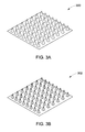
- the nanostructures are conical in shape.
- Fig. 3A schematically illustrates an array of conical nanostructures 300.
- the nanostructures are pyramidal in shape.
- the array of pyramidal nanostructures 302 is illustrated schematically in Fig 3B .
- a pyramid is a polyhedron formed by connecting a polygonal base and a point, called the apex. Each base edge and apex form a triangle. It can be thought of as a conical solid with a polygonal base.
- the polygonal base may take the shape of a triangle, a square, a pentagon, a hexagon, and the like.
- the pyramid may also have a star polygon base.
- the "conical shape” defined herein refers to a figure bounded by a planar base and a surface (lateral surface) formed by the locus of all straight line segments joining the apex to the perimeter of the base.
- the pyramidal or conical nanostructure usually has a continuously varying cross-sectional area along the primary axis.
- the volume fraction of the nanostructure changes with the change in the cross-sectional area.
- the ratio of air to material changes along the primary axis.
- this produces a variation in the effective refractive index along the primary axis of the nanostructure, and results in a graded effective refractive index nanostructure.
- the cross-sectional area of the nanostructure is greater at the lower region, and decreases toward the upper region, as illustrated in Fig. 1 .
- the volume fraction of the nanostructure reduces gradually with the gradual decrease of the cross-sectional area, and increases the air-to-material ratio from the lower region to the upper region.
- the nanostructure usually has a higher refractive index at the lower region that decreases gradually towards the upper region.
- the nanostructures may be relatively narrow or wide, depending on an internal angle of the pyramidal or conical shape.
- the internal angle as used herein may be defined with reference to Fig 2.
- Fig 2 shows a cross-sectional view of a single pyramidal or conical nanostructure on the surface 202 of the substrate 200.
- the nanostructure has the primary axis 204 and 206 is a straight line joining the perimeter of the base to the apex.
- the internal angle 210 is the angle between the axis 204 and the straight line 206.
- the pyramidal or conical nanostructure may have a steep or gentle (shallow) graded effective refractive index.
- the gradient of the effective refractive index depends on the internal angle of the nanostructures.
- the internal angle of the pyramidal or conical nanostructures may be greater than about 1 degree.
- the internal angle may be in a range of from about 1 degree to about 20 degrees, from about 20 degrees to about 40 degrees, from about 40 degrees to about 60 degrees, or from about 60 degrees to about 70 degrees.
- the internal angle may be in a range of from about 20 degrees to about 40 degrees.
- the anti reflection coating includes an array of nanostructures having a graded composition along the primary axis.
- the graded composition of the nanostructure provides the graded refractive index.
- the refractive index changes due to the change in composition of the material of the nanostructure.
- the "graded composition” as defined herein refers to a gradual variation in the composition in one direction, although the gradation may not be always constant.
- the nanostructures may contain a graded composition along the primary axis, in order to provide the graded refractive index.
- the graded composition may comprise a combination of at least two electrically conductive materials. The concentrations of the constituent materials change gradually to achieve the gradation. In another embodiment, the graded composition may be achieved by depositing multiple materials.
- the nanostructures of the graded composition may have a uniform cross-sectional area along the primary axis.
- the cross-sectional area may be of variety of shapes. Examples of various shapes may include, but are not limited to, circular, triangular, rectangular, square, or hexagonal. Irregular shapes are also possible.
- the nanostructures of the graded composition may have non-uniform cross-sectional areas at the lower region and at the upper region.
- the nanostructures may be pyramidal in shape.
- the nanostructures may be conical in shape. In this case, the gradient refractive index of the nanostructure is the combined effect of the gradation in refractive index due to the pyramidal or conical structure, and due to the gradation in the composition.
- the nanostructures have the graded refractive index.
- the refractive index of the nanostructures may gradually vary from the lower region to the upper region.
- the lower region usually has a value, which substantially matches the refractive index of the substrate.
- the type of variation of the refractive index towards the upper region may depend on the presence of a medium (as discussed below) near the upper region.
- the refractive index may increase or decrease in a direction from the lower region to the upper region, and may substantially match the refractive index of the medium in the upper region.
- the refractive index of the nanostructures may decrease in a direction from the lower region to the upper region, as noted previously.
- the value of the refractive index at the upper region may be about 1, which matches the refractive index of the medium. This value may also depend on the material used to form the nanostructure.
- the medium may be air (having a refractive index equal to 1). Therefore, the refractive index of the nanostructures may decrease from the lower region to the upper region in such a way as to attain a lower value at the upper region. In a particular embodiment, the lower value of the refractive index in the upper region may be about 1.
- the array of substantially transparent nanostructures need not be characterized by a graded refractive index.
- each of the nanostructures must have a substantially uniform cross-section along the primary axis.
- the nanostructures are characterized by both a graded refractive index and the substantially uniform cross-section.
- the nanostructures may have a substantially uniform cross-sectional area along the primary axis, as shown in Fig. 4.
- Fig. 4 is a cross-sectional view of the anti-reflection coating disposed on a substrate, according to some embodiments.
- the substrate 400 has a surface 402.
- the anti-reflection coating includes an array of substantially transparent nanostructures 404.
- the nanostructures have a primary axis 406, perpendicular to the surface of the substrate.
- Each of the nanostructures has a lower region 408 and an upper region 410 along the primary axis.
- the lower region 408 is in contact with the surface 402 of the substrate 400.
- the upper region 410 is substantially opposite the lower region 408, on same side of the substrate.
- the nanostructures 404 of the present invention usually have substantially equal cross-sectional areas (412 and 414) at the lower region and at the upper region respectively.
- the nanostructures may be arranged in a random fashion or in a periodic fashion on the surface of the substrate.
- each of the nanostructures is a nanowire. In another embodiment, each of the nanostructures is a nanorod.
- the nanorods may have a height less than about 100 nm, in the above embodiment. In some embodiments, the nanorods may vary in height in a range of from about 50 nm to about 100 nm. Furthermore, the nanorods may be arranged periodically on the surface of the substrate with a period smaller than the wavelength of electromagnetic radiation. Such nanorods of substantially uniform cross-sectional area are characterized by a sub-wavelength scattering phenomenon, and provide very low reflectance. In other words, the nanostructures of the substantially uniform cross-sectional areas may behave as sub-wavelength scattering objects, which provide large forward scattering, and subsequent transmission of light to the underlying substrate. This effect has been shown in absorbing silicon nanowire arrays.
- the nanorods may have a graded composition.
- the reflectance of the anti-reflection coating is the combined effect of the sub wavelength scattering and graded refractive index of the nanorods due to compositional grading.
- the array of substantially transparent nanostructures includes an electrically conductive material.
- suitable, transparent, electrically conductive materials may include an oxide, sulfide, phosphide, telluride or combinations thereof. These transparent electrically conductive materials may be doped or undoped.
- the electrically conductive oxide may include titanium dioxide, silicon oxide, zinc oxide, tin oxide, aluminum doped zinc oxide, fluorine-doped tin oxide, cadmium stannate (tin oxide), and zinc stannate (tin oxide).
- the electrically conductive oxide includes indium containing oxides.
- Suitable indium containing oxides may be selected from the group consisting of indium tin oxide (ITO), Ga-In-Sn-O, Zn-In-Sn-O, Ga-In-O, Zn-In-O, and combinations thereof.
- Suitable sulfides may include cadmium sulfide, indium sulfide and the like.
- Suitable phosphides may include indium phosphide, gallium phosphide, and the like.
- the electrically conductive material may have bandgap greater than about 2.0 eV.
- the nanostructures may contain two or more transparent, electrically conductive materials with gradually varying concentrations
- the array of substantially transparent nanostructures may include a non-conductive non-crystalline material such as glass.
- Non-limiting examples of glasses may include soda-lime glass, alumino-silicate glass, boro-silicate glass, silica, and iron-rich glass.
- the array of substantially transparent nanostructures may include a non-conductive crystalline material.
- each of the nanostructures of the anti-reflection coating may have a height in a range of from about 100 nanometers to about 10 micrometers. In some preferred embodiments, each of the nanostructures may have height in a range of from about 200 nanometers to about 2 micrometers. In one embodiment, each of the nanostructures may have a surface contact area in a range of from about 100 nm 2 to about 10 4 nm 2 . The surface contact area is the cross-sectional area 112 at the lower region of the nanostructure. In some embodiments, the nanostructures may vary in height and surface contact area within the array.
- the substrate may have a substantially planar surface.
- a "substantially planar surface”, as defined herein, usually refers to a substantially flat surface.
- the surface can be smooth, although it may include a relatively minor degree (e.g., about 20% of the total surface area) of texture (e.g., roughness), indentations, and various irregularities.
- the substrate can exhibit flexibility.
- the surface of the substrate may be curved - usually with a relatively large radius of curvature.
- Substrate selection may include substrates of any suitable material, including, but not limited to, metal, semiconductor, doped semiconductor, amorphous dielectrics, crystalline dielectrics, and combinations thereof.
- the substrate includes a transparent and electrically conductive material.
- Suitable transparent, electrically conductive materials may include an oxide, sulfide, phosphide, telluride or combinations thereof. These transparent, electrically conductive materials may be doped or undoped.
- the electrically conductive oxide may comprise titanium dioxide, silicon oxide, zinc oxide, tin oxide, aluminum doped zinc oxide, fluorine-doped tin oxide, cadmium stannate (tin oxide), zinc stannate (tin oxide), or various combinations thereof.
- the electrically conductive oxide includes at least one indium-containing oxide.
- suitable indium-containing oxides are indium tin oxide (ITO), Ga-In-Sn-O, Zn-In-Sn-O, Ga-In-O, Zn-In-O, and combinations thereof.
- Suitable sulfides may include cadmium sulfide, indium sulfide and the like.
- Suitable phosphides may include indium phosphide and the like.
- the electrically conductive material may have a bandgap greater than about 2.0 eV.
- the substrate may comprise a non-conductive non-crystalline material such as glass.
- a non-conductive non-crystalline material such as glass.
- examples of the glass include soda-lime glass, alumino-silicate glass, boro-silicate glass, silica, and, but not limited to, iron-rich glass.
- the substrate may comprise a non-conductive crystalline material.
- the present invention comprises an optoelectronic device.
- the device includes a substrate and an anti-reflection coating.
- the anti-reflection coating is disposed on a surface of the substrate that is positioned for exposure to electromagnetic radiation.
- the anti-reflection coating includes an array of substantially transparent nanostructures having a primary axis.
- the primary axis is substantially perpendicular to the surface of the substrate.
- the array of substantially transparent nanostructures is characterized by a graded refractive index.
- each of the nanostructures has a substantially uniform cross section along the primary axis.
- the "optoelectronic device” refers to devices that either produce light or use light in their operation. Typically, p-n or p-i-n semiconducting junctions are an integral part of optoelectronic devices.
- the optoelectronic devices may be of several types.
- the optoelectronic device may be a photodiode, a light emitting diode, a photovoltaic device, or a semiconductor laser. These optoelectronic devices can be used in variety of applications. Examples of applications include a display, a photo detector, general lighting, a camera, and fiber-optic communications.
- the optoelectronic device is a photovoltaic cell or a photovoltaic module.
- the photovoltaic module may have an array of the photovoltaic cells.
- the photovoltaic module may have glass cover protecting the cells onto which the antireflection coating is disposed.
- the antireflection coating can be disposed on the photovoltaic cells or the photovoltaic module on the surface of the substrate, such that the antireflection coating is exposed to the solar radiation.
- the antireflection coating can be disposed on more than one location of the photovoltaic module, for example, the coating can be disposed on a top side of the module glass cover, a backside of the module glass cover, and/or on a surface of the solar cells in the module, such that the antireflection coating is exposed to the solar radiation.
- the photovoltaic module or the photovoltaic cell may include, but is not limited to, an amorphous silicon cell, a crystalline silicon cell, a hybrid/heterojunction amorphous and crystalline silicon cell, CdTe thin film cell, micromorph tandem silicon thin film cell, Cu(In,Ga)Se 2 (CIGS) thin film cell, GaAs cell, multiple-junction III-V-based solar cells, dye-sensitized solar cells, and solid-state organic/polymer solar cells.
- these solar cells may contain a transparent conductor onto which the anti-reflecting coating is disposed.
- the present invention is directed to a method of forming an anti reflection coating on an optoelectronic device.
- the method includes the steps of forming an array of substantially transparent nanostructures on a surface of a substrate.
- the nanostructures have a primary axis substantially perpendicular to the surface.
- the array of nanostructures is characterized by a graded refractive index.
- each of the nanostructures has a substantially uniform cross section along the primary axis.
- the nanostructures are formed by a technique selected from the group consisting of wet etching, dry etching, and deposition.
- suitable dry etching techniques include, but are not limited to, reactive ion etching (RIE), inductively coupled plasma (ICP) etching, and combinations thereof.
- RIE reactive ion etching
- ICP inductively coupled plasma
- the dry etching technique may be combined with a method of forming nanoscale etch masks.
- the nanoscale etch masks may initially be formed by nanosphere lithography, dip-coating, spin-coating, sputtering, in situ nanoparticle deposition, and combinations thereof. Subsequently, a dry etching step may be performed.
- An example of a suitable wet etching techniques is metal assisted wet etching.
- the deposition technique is selected from the group consisting of chemical vapor deposition, wet chemical solution deposition, physical vapor deposition, and glancing angle deposition technique.
- Glancing angle deposition is known in the art, and described, for example, in " Designing Nanostructures by Glancing Angle Deposition” by Y. P. Zhao et al, Proceedings of SIPE Vol. 5219 Nanotubes and Nanowires; SPIE, Bellingham, WA, 2003 .
- the glancing angle deposition (GLAD) technique is usually carried out by combining oblique angle deposition with substrate positional control.
- GLAD involves a physical vapor deposition process, where the deposition flux is incident onto a substrate with a large angle with respect to the surface normal, while the substrate is rotating.
- GLAD produces columnar structures through the effect of shadowing during film growth, while the substrate rotation controls the shape of the columns.
- GLAD provides three parameters - the incident angle, the growth rate and the substrate rotational speed, to control the morphology of the nanostructures.
- the deposition rate not only has a vertical component (with respect to the substrate), but also has a lateral component.
- the lateral growth rate contributes to the shadowing effect, which gives rise to two major advantages for GLAD: the self-alignment effect and the lateral sculpturing effect.
- the example illustrates an embodiment where a deposition technique was used to produce the anti reflection coating.
- This involved growing Si nanostructures on a quartz substrate, using the vapor-liquid-solid growth mechanism (VLS) with chemical vapor deposition (CVD).
- VLS vapor-liquid-solid growth mechanism
- CVD chemical vapor deposition
- the techniques to grow nanostructures are described, for example, in “ Vapor-liquid-solid mechanism of single crystal growth,” by R. S. Wagner et al, Appl. Phys. Lett. 4(5), 89-90 (1964 ) and in " Conformal Dielectric Films on Silicon Nanowire Arrays by Plasma Enhanced Chemical Vapor Deposition", J. Fronheiser, et al, Journal of Nanoparticle Research, (2008 ).
- nanostructures in this manner at high temperatures (greater than about 700 °C), using silane and hydrogen gas precursors, led to pyramidal or conical shapes having a larger cross-sectional area at the base than that of the top due to enhanced sidewall deposition.
- the nanostructures have lengths of about 2-5 microns and diameters of about 50-200 nm.
- the nanostructures were subsequently oxidized in a tube furnace containing oxygen at 600-800 °C.
- ZnO nanostructures were formed by solution deposition at 70-90 °C on a glass substrate coated with a thin ZnO seed layer.
- Well-formed, high density arrays of nanostructures were fashioned with lengths up to 3 micrometers.
- a metal assisted galvanic wet etching technique was used to produce the array of nanostructures.
- a silicon film was disposed over the substrate of the optoelectronic device.
- the device (or the substrate) was then placed in a chemical bath with anisotropic etchant and a metal precursor (1M AgNO 3 in HF).
- the temperature of the bath was kept between 50-80 °C. This process led to the precipitation of nanoscale Ag dendrite particles on the surface.
- the Si nanostructures were then oxidized to form transparent silicon oxide nanostructures.
- Nanosphere lithography was combined with reactive ion etching (RIE) to form nanostructured anti-reflective layers on a glass substrate.
- RIE reactive ion etching
- Nanosphere lithography is well known and described, for example, in " Nanosphere lithography: A materials general fabrication process for periodic particle array surfaces", J.C. Hulteen et al, J. Vac. Sci. Technol. A, 13 1553 (1995 ).
- a fused silica substrate was coated with a 1 micrometer thick amorphous silica layer by high temperature low-pressure chemical vapor deposition.
- Nanosphere lithography was performed by dipping the substrates in a solution containing polystyrene nanospheres such that the nanospheres assembled into a hexagonal close-packed monolayer lattice on the glass surface when removed from the solution.
- a 100 nm Ni film was then electron-beam evaporated onto the samples, such that Ni nanoscale dots/triangles were formed on the glass substrates in the location below the interstices of the nanospheres.
- the nanospheres were removed from the surface by soaking in acetone to allow for lift-off.
- Nanostructures arrays were formed by placing the samples in an RIE reactor using a standard oxide etch recipe targeting a 2 micron etch depth.
- a similar process can be performed directly on a soda-lime glass or a substrate containing a transparent conductor.
- the nanoscale etch masks have also been formed by direct deposition and annealing of a thin metal Ni film.
- the measured total reflectance and transmission properties of the silica nanostructrures were found to be up to 50% better than the control substrates without nanostructures over the whole spectral range from 300 to 1,100 nm.
- nanowires with a graded composition along the primary axis were produced.
- the array of graded composition nanowires was achieved by glancing angle deposition. Multiple compositions of Si 1-x Ti x O 2 for different values of x were deposited.
- the initial feed composition contained only TiO 2 .
- the amount of TiO 2 was decreased while equal amounts of SiO 2 were added, so that at the end of deposition, i.e., at the top of the nanostructures, the composition was purely SiO 2 .
- Similar grading may also be achieved by chemical vapor deposition or by liquid phase synthesis, followed by nanostructure formation with wet or dry etching techniques.
Landscapes
- Physics & Mathematics (AREA)
- General Physics & Mathematics (AREA)
- Optics & Photonics (AREA)
- Surface Treatment Of Optical Elements (AREA)
- Laminated Bodies (AREA)
Applications Claiming Priority (1)
| Application Number | Priority Date | Filing Date | Title |
|---|---|---|---|
| US12/421,101 US20100259823A1 (en) | 2009-04-09 | 2009-04-09 | Nanostructured anti-reflection coatings and associated methods and devices |
Publications (2)
| Publication Number | Publication Date |
|---|---|
| EP2241909A2 true EP2241909A2 (de) | 2010-10-20 |
| EP2241909A3 EP2241909A3 (de) | 2011-03-09 |
Family
ID=42262640
Family Applications (1)
| Application Number | Title | Priority Date | Filing Date |
|---|---|---|---|
| EP10157871A Withdrawn EP2241909A3 (de) | 2009-04-09 | 2010-03-26 | Nanostrukturierte Antireflexionsbeschichtungen und zugehörige Verfahren und Vorrichtungen |
Country Status (4)
| Country | Link |
|---|---|
| US (1) | US20100259823A1 (de) |
| EP (1) | EP2241909A3 (de) |
| CN (1) | CN101858995A (de) |
| AU (1) | AU2010201388A1 (de) |
Cited By (3)
| Publication number | Priority date | Publication date | Assignee | Title |
|---|---|---|---|---|
| WO2012151097A1 (en) * | 2011-05-02 | 2012-11-08 | Corning Incorporated | Glass article having antireflective layer and method of making |
| WO2015193082A1 (de) * | 2014-06-18 | 2015-12-23 | Robert Bosch Gmbh | Verfahren zum herstellen einer nanostruktur in einem transparenten substrat |
| US10935702B2 (en) * | 2018-04-02 | 2021-03-02 | Northrop Grumman Systems Corporation | Reflection and diffraction control with slanted semiconductor metamaterials |
Families Citing this family (42)
| Publication number | Priority date | Publication date | Assignee | Title |
|---|---|---|---|---|
| US20090287733A1 (en) * | 2008-05-15 | 2009-11-19 | Chanan Steinhart | Method for preparing prepress image data |
| US8574710B2 (en) * | 2008-10-10 | 2013-11-05 | Nano Terra Inc. | Anti-reflective coatings comprising ordered layers of nanowires and methods of making and using the same |
| US20110290316A1 (en) * | 2010-05-28 | 2011-12-01 | Daniel Warren Hawtof | Light scattering inorganic substrates by soot deposition |
| WO2012020899A1 (ko) * | 2010-08-10 | 2012-02-16 | 연세대학교 산학협력단 | 반사 방지성 유리 및 그 제조 방법 |
| US8445309B2 (en) | 2010-08-20 | 2013-05-21 | First Solar, Inc. | Anti-reflective photovoltaic module |
| CN102033255B (zh) * | 2010-10-26 | 2012-02-29 | 中国科学院苏州纳米技术与纳米仿生研究所 | 一种宽谱广角增透亚波长结构的制备方法 |
| CN102074591A (zh) * | 2010-12-02 | 2011-05-25 | 中国科学院苏州纳米技术与纳米仿生研究所 | 用于太阳电池吸收增强的复合微纳光子结构及其制法 |
| CN102097497A (zh) * | 2010-12-27 | 2011-06-15 | 重庆大学 | 一种高转换效率的太阳能电池 |
| CN102169195A (zh) * | 2011-01-24 | 2011-08-31 | 中国科学院苏州纳米技术与纳米仿生研究所 | 纳米减反薄膜或增透膜以及光学或光电器件的制备方法 |
| US8842265B2 (en) | 2011-04-19 | 2014-09-23 | Hewlett-Packard Development Company, L.P. | Configurable grating based on collapsing nano-fingers |
| US20150064405A1 (en) * | 2011-04-20 | 2015-03-05 | Corning Incorporated | Low reflectivity articles and methods thereof |
| US9447492B2 (en) | 2011-06-03 | 2016-09-20 | Graham J. Hubbard | Conductive anti-reflective films |
| TWI424583B (zh) * | 2011-07-25 | 2014-01-21 | 國立清華大學 | 薄膜太陽能電池的製造方法 |
| WO2013171286A1 (en) * | 2012-05-15 | 2013-11-21 | Danmarks Tekniske Universitet | Solar cells having a nanostructured antireflection layer |
| CN102842623A (zh) * | 2012-06-29 | 2012-12-26 | 法国圣戈班玻璃公司 | 光学组件及其制造方法、光伏器件 |
| JP6371032B2 (ja) * | 2012-08-01 | 2018-08-08 | スリーエム イノベイティブ プロパティズ カンパニー | 反射防止ハードコートおよび反射防止物品 |
| WO2014121505A1 (en) * | 2013-02-07 | 2014-08-14 | Nano And Advanced Materials Institute Limited | Silica nanowires for in-coupling to organic photovoltaic cells |
| US9268097B2 (en) * | 2013-05-03 | 2016-02-23 | TeraDiode, Inc. | High power optical fiber ends having partially-doped gratings |
| CN103253870B (zh) * | 2013-05-14 | 2016-03-02 | 青岛博纳光电装备有限公司 | 一种抗反射和自清洁玻璃及其制造方法 |
| US20160293781A1 (en) * | 2013-11-21 | 2016-10-06 | The Hong Kong University Of Science And Technology | Three dimensional anti-reflection nanocone film |
| CN104319299A (zh) * | 2014-08-29 | 2015-01-28 | 叶瑾琳 | 反向导电纳米阵列及其制造方法 |
| JPWO2016047032A1 (ja) * | 2014-09-25 | 2017-07-13 | パナソニックIpマネジメント株式会社 | 光学部材、その製造方法及び撮像装置 |
| JP6338503B2 (ja) * | 2014-09-30 | 2018-06-06 | 富士フイルム株式会社 | 光学素子および光学素子の製造方法 |
| CN104600129A (zh) * | 2014-12-26 | 2015-05-06 | 上海科慧太阳能技术有限公司 | 减反射膜及其制备方法以及具有减反射膜的太阳能电池 |
| KR101765008B1 (ko) | 2016-04-29 | 2017-08-04 | 선문대학교 산학협력단 | 태양전지용 판넬 및 이의 제조방법 |
| US10401535B2 (en) | 2016-07-25 | 2019-09-03 | Apple Inc. | Electronic devices having transparent crystalline structures with antireflection coatings |
| US10995624B2 (en) | 2016-08-01 | 2021-05-04 | General Electric Company | Article for high temperature service |
| CN106352903A (zh) * | 2016-08-19 | 2017-01-25 | 深圳市金立通信设备有限公司 | 一种光传感器、终端以及光传感器的安装方法 |
| CN106526716B (zh) * | 2016-11-22 | 2018-06-22 | 武汉华星光电技术有限公司 | 一种微纳结构减反膜的制作方法及显示装置 |
| CN109196388A (zh) * | 2017-03-13 | 2019-01-11 | 京东方科技集团股份有限公司 | 抗反射涂层、触控基板、显示装置和制造抗反射涂层的方法 |
| JP7222674B2 (ja) * | 2017-12-15 | 2023-02-15 | 信越化学工業株式会社 | 反射防止膜、反射防止膜の製造方法、及び眼鏡型ディスプレイ |
| CN108227376A (zh) * | 2018-01-03 | 2018-06-29 | 京东方科技集团股份有限公司 | 一种微结构的制备方法、压印模版、显示基板 |
| WO2019170357A1 (en) | 2018-03-06 | 2019-09-12 | Asml Holding N.V. | Anti-reflection optical substrates and methods of manufacture |
| CN108866513B (zh) * | 2018-09-13 | 2020-12-18 | 德淮半导体有限公司 | 一种化学气相沉积工艺 |
| US11487139B2 (en) | 2018-11-27 | 2022-11-01 | Applied Materials, Inc. | Nanostructures for optical devices |
| EP3918390A4 (de) * | 2019-01-28 | 2022-10-05 | B.G. Negev Technologies and Applications Ltd., at Ben-Gurion University | Struktur für eine wellenleiterfacette |
| CN111739954A (zh) * | 2020-06-30 | 2020-10-02 | 苏州大学 | 晶硅太阳能电池及其制备方法 |
| US12382748B2 (en) * | 2021-01-04 | 2025-08-05 | Saudi Arabian Oil Company | Nanostructures to reduce optical losses |
| CN116940866A (zh) * | 2021-01-06 | 2023-10-24 | 梅特兰兹股份有限公司 | 自对准纳米柱涂层及其制造方法 |
| FR3124023B1 (fr) * | 2021-06-15 | 2023-06-02 | David J Rogers | Revêtement anti-éblouissement de nanostructure d’oxyde à large bande interdite et son utilisation |
| EP4279460A1 (de) | 2022-05-17 | 2023-11-22 | Kaunas University of Technology | Multifunktionale selbstreinigende nanobeschichtung |
| CN119065034A (zh) * | 2024-09-14 | 2024-12-03 | 中国科学院上海微系统与信息技术研究所 | 一种超表面单元及微纳光子器件 |
Family Cites Families (21)
| Publication number | Priority date | Publication date | Assignee | Title |
|---|---|---|---|---|
| US4190321A (en) * | 1977-02-18 | 1980-02-26 | Minnesota Mining And Manufacturing Company | Microstructured transmission and reflectance modifying coating |
| US4340276A (en) * | 1978-11-01 | 1982-07-20 | Minnesota Mining And Manufacturing Company | Method of producing a microstructured surface and the article produced thereby |
| CN1057611C (zh) * | 1993-08-31 | 2000-10-18 | 住友水泥株式会社 | 抗反射膜 |
| US5811191A (en) * | 1994-12-27 | 1998-09-22 | Ppg Industries, Inc. | Multilayer antireflective coating with a graded base layer |
| JP3368225B2 (ja) * | 1999-03-11 | 2003-01-20 | キヤノン株式会社 | 回折光学素子の製造方法 |
| CN1285098C (zh) * | 2001-06-29 | 2006-11-15 | 美莎诺普有限公司 | 光电子器件集成 |
| US20030215626A1 (en) * | 2002-03-22 | 2003-11-20 | Hiller Jeri?Apos;Ann | Nanoporous coatings |
| JP2003279705A (ja) * | 2002-03-25 | 2003-10-02 | Sanyo Electric Co Ltd | 反射防止部材 |
| DE60333715D1 (de) * | 2002-10-30 | 2010-09-23 | Hitachi Ltd | Verfahren zur Herstellung funktioneller Substrate, die kolumnare Mikrosäulen aufweisen |
| US6940651B2 (en) * | 2002-12-30 | 2005-09-06 | Eitan Zeira | Durable nano-structured optical surface |
| DE60326121D1 (de) * | 2003-05-20 | 2009-03-26 | Dsm Ip Assets Bv | Verfahren zur Herstellung von Nanostrukturierten Oberflächenbeschichtungen, deren Beschichtungen und Gegenständen enthaltend die Beschichtung |
| US7132677B2 (en) * | 2004-02-13 | 2006-11-07 | Dongguk University | Super bright light emitting diode of nanorod array structure having InGaN quantum well and method for manufacturing the same |
| WO2006059686A1 (ja) * | 2004-12-03 | 2006-06-08 | Sharp Kabushiki Kaisha | 反射防止材、光学素子、および表示装置ならびにスタンパの製造方法およびスタンパを用いた反射防止材の製造方法 |
| US20060207647A1 (en) * | 2005-03-16 | 2006-09-21 | General Electric Company | High efficiency inorganic nanorod-enhanced photovoltaic devices |
| EP1750310A3 (de) * | 2005-08-03 | 2009-07-15 | Samsung Electro-Mechanics Co., Ltd. | Reflektor mit kugelförmiger Richtcharakteristik und Leuchttdiode versehen mit einem solchen Reflektor |
| SG150516A1 (en) * | 2005-08-12 | 2009-03-30 | Cambrios Technologies Corp | Nanowires-based transparent conductors |
| US20070169808A1 (en) * | 2006-01-26 | 2007-07-26 | Kherani Nazir P | Solar cell |
| DE102006046131B4 (de) * | 2006-09-28 | 2020-06-25 | X-Fab Semiconductor Foundries Ag | Verfahren zur Herstellung einer optischen Schnittstelle für integrierte Optikanwendungen |
| WO2008069223A1 (en) * | 2006-12-05 | 2008-06-12 | Semiconductor Energy Laboratory Co., Ltd. | Anti-reflection film and display device |
| US20080185041A1 (en) * | 2007-02-02 | 2008-08-07 | Guardian Industries Corp. | Method of making a photovoltaic device with antireflective coating containing porous silica and resulting product |
| WO2008148462A1 (en) * | 2007-06-05 | 2008-12-11 | Carl Zeiss Smt Ag | Methods for producing an antireflection surface on an optical element, optical element and associated optical arrangement |
-
2009
- 2009-04-09 US US12/421,101 patent/US20100259823A1/en not_active Abandoned
-
2010
- 2010-03-26 EP EP10157871A patent/EP2241909A3/de not_active Withdrawn
- 2010-04-07 AU AU2010201388A patent/AU2010201388A1/en not_active Abandoned
- 2010-04-09 CN CN201010165182A patent/CN101858995A/zh active Pending
Non-Patent Citations (9)
| Title |
|---|
| A. REYES-CORONADO ET AL.: "Measurement of the effective refractive index of a turbid colloidal suspension using light refraction", NEW JOURNAL OF PHYSICS, vol. 7, 2005, pages 89 |
| B. S. LUK'YANCHUK: "Peculiarities of light scattering by nanoparticles and nanowires near plasmon resonance frequencies in weakly dissipating materials", J. OPT. A: PURE APPLIED OPTICS, vol. 9, 2007, pages S294 - S300 |
| J. FRONHEISER ET AL.: "Conformal Dielectric Films on Silicon Nanowire Arrays by Plasma Enhanced Chemical Vapor Deposition", JOURNAL OF NANOPARTICLE RESEARCH, 2008 |
| J.C. HULTEEN ET AL.: "Nanosphere lithography: A materials general fabrication process for periodic particle array surfaces", J. VAC. SCI. TECHNOL., vol. A, 1995, pages 13 1553 |
| J.-Q. XI ET AL.: "Optical Thin-Film Materials With Low Refractive Index For Broadband Elimination Of Fresnel Reflection", NATURE PHOTONICS, vol. 1, 2007, pages 176 |
| L. TSAKALAKOS ET AL.: "Strong Broadband Optical Absorption in Si Nanowire Films", JOURNAL OF NANOPHOTONICS, vol. 1, 17 July 2007 (2007-07-17) |
| MUSKENS O L ET AL: "EPITAXIAL GROWTH OF ALIGNED SEMICONDUCTOR NANOWIRE METAMATERIALS FOR PHOTONIC APPLICATIONS", ADVANCED FUNCTIONAL MATERIALS, WILEY - V C H VERLAG GMBH & CO. KGAA, DE, vol. 18, no. 7, 11 April 2008 (2008-04-11), pages 1039 - 1046, XP001511808, ISSN: 1616-301X, DOI: 10.1002/ADFM.200701337 * |
| R. S. WAGNER ET AL.: "Vapor-liquid-solid mechanism of single crystal growth", APPL. PHYS. LETT., vol. 4, no. 5, 1964, pages 89 - 90 |
| Y. P. ZHAO ET AL.: "Designing Nanostructures by Glancing Angle Deposition", PROCEEDINGS OF SIPE, vol. 5219 |
Cited By (7)
| Publication number | Priority date | Publication date | Assignee | Title |
|---|---|---|---|---|
| WO2012151097A1 (en) * | 2011-05-02 | 2012-11-08 | Corning Incorporated | Glass article having antireflective layer and method of making |
| US9272947B2 (en) | 2011-05-02 | 2016-03-01 | Corning Incorporated | Glass article having antireflective layer and method of making |
| WO2015193082A1 (de) * | 2014-06-18 | 2015-12-23 | Robert Bosch Gmbh | Verfahren zum herstellen einer nanostruktur in einem transparenten substrat |
| US20170131437A1 (en) * | 2014-06-18 | 2017-05-11 | Robert Bosch Gmbh | Method for creating a nanostructure in a transparent substrate |
| US10663624B2 (en) | 2014-06-18 | 2020-05-26 | Robert Bosch Gmbh | Method for creating a nanostructure in a transparent substrate |
| DE102014211753B4 (de) | 2014-06-18 | 2024-02-08 | Robert Bosch Gmbh | Verfahren zum Herstellen einer Nanostruktur in einem transparenten Substrat |
| US10935702B2 (en) * | 2018-04-02 | 2021-03-02 | Northrop Grumman Systems Corporation | Reflection and diffraction control with slanted semiconductor metamaterials |
Also Published As
| Publication number | Publication date |
|---|---|
| AU2010201388A1 (en) | 2010-10-28 |
| US20100259823A1 (en) | 2010-10-14 |
| CN101858995A (zh) | 2010-10-13 |
| EP2241909A3 (de) | 2011-03-09 |
Similar Documents
| Publication | Publication Date | Title |
|---|---|---|
| US20100259823A1 (en) | Nanostructured anti-reflection coatings and associated methods and devices | |
| CN101958347B (zh) | 纳米结构功能涂层和器件 | |
| Hua et al. | Efficient photon management with nanostructures for photovoltaics | |
| Soueiti et al. | A review of cost-effective black silicon fabrication techniques and applications | |
| Srivastava et al. | Excellent antireflection properties of vertical silicon nanowire arrays | |
| Moayedfar et al. | Various types of anti-reflective coatings (ARCS) based on the layer composition and surface topography: a review | |
| Zhu et al. | Nanostructured photon management for high performance solar cells | |
| Sanchez-Sobrado et al. | Colloidal-lithographed TiO 2 photonic nanostructures for solar cell light trapping | |
| US10843923B2 (en) | Property control of multifunctional surfaces | |
| Sanchez-Sobrado et al. | Lightwave trapping in thin film solar cells with improved photonic-structured front contacts | |
| KR20120012555A (ko) | 점진적으로 굴절률이 변하는 실리콘 다층 무반사막 및 그 제조방법 및 이를 구비하는 태양전지 및 그 제조방법 | |
| CN110249240A (zh) | 具有提高的效率的太阳能电池及其制备方法 | |
| WO2013171286A1 (en) | Solar cells having a nanostructured antireflection layer | |
| Tan et al. | Combined optical and electrical design of plasmonic back reflector for high-efficiency thin-film silicon solar cells | |
| Lin et al. | Packaging glass with a hierarchically nanostructured surface: a universal method to achieve self-cleaning omnidirectional solar cells | |
| US20150107660A1 (en) | Super-Transparent Electrodes for Photovoltaic Applications | |
| Nichkalo et al. | Fabrication and characterization of high-performance anti-reflecting nanotextured Si surfaces for solar cells | |
| US10475940B2 (en) | Packaging glass with hierarchically nanostructured surface | |
| KR101773951B1 (ko) | 반도체 기판의 텍스쳐링 방법, 이 방법에 의해 제조된 반도체 기판 및 이를 포함하는 디바이스 | |
| Kasar et al. | Surface Engineering of Solar Cells to Improve Efficiency: Kasar and Menezes | |
| Nebol’sin et al. | Black silicon: a new manufacturing method and optical properties | |
| CN103035752B (zh) | 包含纳米结构抗反膜的晶体硅太阳能电池及其制备方法 | |
| Wang et al. | Design and fabrication of new wide-band and wide-angle solar cell absorbing layer | |
| Badán et al. | Optical properties of Si nanowires: Dependence on substrate crystallographic orientation and light polarization | |
| JP2013030805A (ja) | 単粒子膜エッチングマスクを有する表面微細凹凸構造体形成基板の製法 |
Legal Events
| Date | Code | Title | Description |
|---|---|---|---|
| PUAI | Public reference made under article 153(3) epc to a published international application that has entered the european phase |
Free format text: ORIGINAL CODE: 0009012 |
|
| AK | Designated contracting states |
Kind code of ref document: A2 Designated state(s): AT BE BG CH CY CZ DE DK EE ES FI FR GB GR HR HU IE IS IT LI LT LU LV MC MK MT NL NO PL PT RO SE SI SK SM TR |
|
| AX | Request for extension of the european patent |
Extension state: AL BA ME RS |
|
| PUAL | Search report despatched |
Free format text: ORIGINAL CODE: 0009013 |
|
| AK | Designated contracting states |
Kind code of ref document: A3 Designated state(s): AT BE BG CH CY CZ DE DK EE ES FI FR GB GR HR HU IE IS IT LI LT LU LV MC MK MT NL NO PL PT RO SE SI SK SM TR |
|
| AX | Request for extension of the european patent |
Extension state: AL BA ME RS |
|
| 17P | Request for examination filed |
Effective date: 20110909 |
|
| 17Q | First examination report despatched |
Effective date: 20120522 |
|
| STAA | Information on the status of an ep patent application or granted ep patent |
Free format text: STATUS: THE APPLICATION IS DEEMED TO BE WITHDRAWN |
|
| 18D | Application deemed to be withdrawn |
Effective date: 20121002 |