EP2242077B1 - Attribution d'espace dans un disjoncteur - Google Patents
Attribution d'espace dans un disjoncteur Download PDFInfo
- Publication number
- EP2242077B1 EP2242077B1 EP10160205.0A EP10160205A EP2242077B1 EP 2242077 B1 EP2242077 B1 EP 2242077B1 EP 10160205 A EP10160205 A EP 10160205A EP 2242077 B1 EP2242077 B1 EP 2242077B1
- Authority
- EP
- European Patent Office
- Prior art keywords
- circuit breaker
- circuit
- disposed
- section
- protection device
- Prior art date
- Legal status (The legal status is an assumption and is not a legal conclusion. Google has not performed a legal analysis and makes no representation as to the accuracy of the status listed.)
- Active
Links
Images










Classifications
-
- H—ELECTRICITY
- H01—ELECTRIC ELEMENTS
- H01H—ELECTRIC SWITCHES; RELAYS; SELECTORS; EMERGENCY PROTECTIVE DEVICES
- H01H71/00—Details of the protective switches or relays covered by groups H01H73/00 - H01H83/00
- H01H71/02—Housings; Casings; Bases; Mountings
- H01H71/0207—Mounting or assembling the different parts of the circuit breaker
-
- H—ELECTRICITY
- H01—ELECTRIC ELEMENTS
- H01H—ELECTRIC SWITCHES; RELAYS; SELECTORS; EMERGENCY PROTECTIVE DEVICES
- H01H83/00—Protective switches, e.g. circuit-breaking switches, or protective relays operated by abnormal electrical conditions otherwise than solely by excess current
- H01H83/20—Protective switches, e.g. circuit-breaking switches, or protective relays operated by abnormal electrical conditions otherwise than solely by excess current operated by excess current as well as by some other abnormal electrical condition
-
- H—ELECTRICITY
- H01—ELECTRIC ELEMENTS
- H01H—ELECTRIC SWITCHES; RELAYS; SELECTORS; EMERGENCY PROTECTIVE DEVICES
- H01H83/00—Protective switches, e.g. circuit-breaking switches, or protective relays operated by abnormal electrical conditions otherwise than solely by excess current
- H01H83/20—Protective switches, e.g. circuit-breaking switches, or protective relays operated by abnormal electrical conditions otherwise than solely by excess current operated by excess current as well as by some other abnormal electrical condition
- H01H83/22—Protective switches, e.g. circuit-breaking switches, or protective relays operated by abnormal electrical conditions otherwise than solely by excess current operated by excess current as well as by some other abnormal electrical condition the other condition being imbalance of two or more currents or voltages
- H01H83/226—Protective switches, e.g. circuit-breaking switches, or protective relays operated by abnormal electrical conditions otherwise than solely by excess current operated by excess current as well as by some other abnormal electrical condition the other condition being imbalance of two or more currents or voltages with differential transformer
Definitions
- the subject matter disclosed herein relates to circuit breakers. More particularly, to space allocation within the housing of a circuit breaker, and an interface to trip the circuit breaker.
- a conventional electronic residual current circuit breaker with overcurrent protection (“eRCBO”) includes single housing configured to provide a miniature circuit breaker (MCB) portion and a residual current (for example, a ground fault) device (RCD) portion for providing combined protection from the risk of electrocution and protection against the risk of an electrical fire and overcurrent protection of equipment and cables.
- eRCBO electronic residual current circuit breaker with overcurrent protection
- MBC circuit breaker
- RCD ground fault
- a typical conventional eRCBO is of a size of approximately 125 mm in height, 18 mm in width and 70 mm deep.
- the housing is multi-sectional and includes an interior wall dividing the space within the housing to provide equal or unequal distribution of the space within the eRCBO.
- a circuit breaker according to claim 1 is disclosed.
- the circuit breaker 100 for providing overcurrent and short-circuit protection is disclosed.
- the circuit breaker 100 has a current rating of approximately 6 to 40A with a short circuit (SC) capacity of approximately 6KA, for example.
- SC short circuit
- the present invention is not limited to any particular electrical ratings and may vary accordingly.
- the circuit breaker includes a single pole module 110 and a test assembly 112 arranged to allow a user to simulate a residual current fault situation for performing a test operation of a tripping mechanism of the circuit breaker 100.
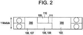
- Fig. 2 is an orthographic layout of a module of the circuit breaker in accordance with an embodiment of the present invention.
- the single pole module 110 is approximately 86mm in height, 18mm in width and 70 mm in depth, for example.
- the module 110 of the present invention is not limited to any particular dimensions and may vary accordingly.
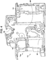
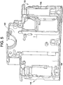
- the module 110 includes an interior wall 111 (as depicted in Fig. 2 ), which divides the space within the circuit breaker 100 and serves as a shell or frame onto which components of the circuit breaker 100 are disposed. Details regarding the module 110 will now be described with reference to Figs. 2 through 6 . As shown in Fig.
- the module 110 includes a first portion (i.e., an RCD side 200) having a first current path region and a second portion (i.e., an MCB pole side 300) adjacent to the second current path region and having a second current path region.
- the interior wall 111 separates the first portion from the second portion.
- the RCD side 200 of the module 110 includes a first section 103 configured to receive a printed circuit board 201 (as depicted in Fig. 7 ) and a second section 105 configured to receive a lever mechanism 207 (as depicted in Fig. 7 ).
- the lever mechanism 207 is in operable communication with the PCB 201 to perform a trip operation of the circuit breaker 100. Additional details regarding the operation of the lever mechanism 207 will be discussed below with reference to Figs. 7 through 9 .
- the MCB pole side 300 of the module 110 includes a first section 106 configured to receive an electromagnetic protection device 306 (as depicted in Fig. 9 ), a second section 107 configured to receive an arc distinguishing device 307 (as depicted in Fig. 9 ), a third section 108 configured to receive a thermal protection device 308 (as depicted in Fig. 9 ), and a fourth section 109 configured to receive an operating mechanism 302 (as depicted in Fig. 9 ).
- the first section 103 and the second section 105 of the RCD side 200 occupy substantially half of the module 110 and the first section 106, the second section 107, the third section 108 and the fourth section 109 of the MCB pole side 300 occupy substantially half of the module 110.
- the second section 105 of the RCD side 200 and the third and fourth sections 108 and 109 of the MCB pole side 300 are disposed opposite each other. Further, the second section 105 of the RCD side 200 and the third and fourth sections 108 and 109 of the MCB pole side 300 are also centrally disposed within the module 110 relative to a length of the module 110.
- the first section 103 of the RCD side 200 and the first and second sections 106 and 107 of the MCB pole side 300 together occupy a substantial part of an internal width of the module 110.
- the first section 103 of the RCD side 200 is disposed at an opposite end relative to the length of the module 110 from the first and second sections 106 and 107 of the MCB pole side 300.
- the second section 105 of the RCD side 200 and the third and fourth sections 108 and 109 of the MCB pole side 300 are disposed in between the first section 103 of the RCD side 200 and the first and second sections 106 and 107 of the MCB pole side 300.
- the first portion of the module 110 which houses the RCD side 200 forms an L-shape
- the second portion of the module 110 forms an L-shape.
- the first portion and the second portion comprise substantially total area of the module 110.
- the module 110 includes a first circuit connection portion 113 and a second connection portion 115.
- the first circuit connection portion 113 includes an open portion 114a adjacent to the first section 106 of the MCB pole side 300 and is configured to receive a phase conductor of the circuit breaker 100.
- the module 110 includes a molded enclosure 114b configured to receive a phase conductor of the circuit breaker 100. Additional details regarding the first and second circuit connection portions 113 and 115 will be discussed below.
- the RCD side 200 is arranged on one side for use in conjunction with the MCB pole side 300. Details regarding the RCD side 200 and the MCB pole side 300 will now be described below in reference to Figs. 7 and 9 .
- Fig. 7 is a schematic diagram illustrating the RCD side 200 of the circuit breaker 100.
- the RCD side 200 includes a printed circuit board (PCB) 201 having a trip solenoid 203 disposed within the first section 103 of the module 110.
- the PCB 201 further includes a current transformer 205 along with other electrical and electronic components.
- the current transformer 205 monitors current flow in the circuit breaker 100.
- the PCB 201 is housed within the first portion of the single pole module 110.
- the PCB 201 is centrally disposed relative to the height of the circuit breaker 100.
- the trip solenoid 203 includes an elongated body and is mounted within the PCB 201 such that a length of the elongated body is aligned with the depth of the single pole module 110.
- the current transformer 205 straddles the PCB 201 at an end portion of the PCB 201 opposite that of the trip solenoid 203.
- the present invention is not limited to any particular arrangement of the trip solenoid 203 and the current transformer 205, and may vary as necessary. Alternative embodiments will be discussed below with reference to Figs. 12 and 15 .
- the RCD side 200 further includes a lever mechanism 207 in operable communication with the trip solenoid 203.
- the lever mechanism 207 includes an end portion configured to be in operable communication with the trip solenoid 203.
- the lever mechanism 207 is disposed at a center portion of the module 110 adjacent to test assembly 112.
- Fig. 8 is a perspective view illustrating the lever mechanism 207 shown in Fig. 7 in accordance with an embodiment of the present invention.
- the lever mechanism 207 includes a pin 207a on a side thereof facing the interior wall 111 and inserted through the interior wall 111 to extend to the other side (i.e., the MCB pole side 300) of the circuit breaker 100.
- the pin 207a interfaces with an activator 317 disposed on the MCB pole side 300 (as depicted in FIG. 9 ). Additional details regarding the interface between the lever mechanism 207 and the activator 317 will be discussed below.
- the single pole module 110 further includes end portions at each end for circuit connections.
- the first circuit connection portion 113 is adjacent to a circuit protection device 305 (as depicted in Fig. 9 ) and the second terminal portion 115 is adjacent to the PCB 201.
- first and second circuit connection portions 113 and 115 are screw-operated terminals.
- the present invention is not limited hereto and may vary accordingly. Additional details regarding the first and second circuit connection portions 113 and 115 will be described below with reference to Figs. 10 through 15 .
- a solenoid plunger (not shown) of the trip solenoid 203 moves in a direction as indicated by arrow 1, and the lever mechanism 207 is actuated by the trip solenoid 203.
- the lever mechanism 207 rotates in a clockwise direction about a pin 209 (as indicated by arrow 2).
- the lever mechanism 207 acts as an interface between the RCD side 200 and the MCB pole side 300 to enable a trip operation of the circuit breaker 100. Additional details regarding the operation of the lever mechanism 207 and its interface to the MCB pole side 300 will be discussed below with reference to Fig 9 .
- Fig. 9 is a schematic diagram illustrating the MCB pole side 300 of the circuit breaker 100 according to an embodiment of the present invention.
- a toggle lever 301 is in mechanical communication with an operating mechanism 302 to control the position of a movable contact arm 304.
- the operating mechanism 302 is disposed in the fourth section 109 of the MCB pole side 300 of the module 110.
- a circuit protection device 305 is also provided.
- a tripping mechanism 309 in operable communication with the circuit protection device 305 is also provided for tripping the circuit breaker 100.
- the circuit protection device 305 includes an electromagnetic protection device 306 (i.e., a coil) for short circuit protection, an arc distinguishing device 307 to extinguish arcs created during the trip operation of the circuit breaker 100 and a thermal protection device 308 for over current protection.
- the electromagnetic protection device 306 is disposed in the first section 106
- the arc distinguishing device 307 is disposed in the second section 107
- the thermal protection device 308 is disposed in the third section 108 of the MCB pole side 300.
- the MCB pole side 300 further includes an external tripping lever 311.
- the movable contact arm 304 is shown in a "closed" position, which corresponds to an "on” position of the toggle lever 301, to allow the current to flow through the circuit breaker 100.
- Current flows from a fixed contact 312 to a movable contact 313 disposed on the movable contact arm 304.
- a spring 315 is connected with a second end 116b of the axle 116 and is in operable communication with the movable contact arm 304.
- the activator 317 is in operable communication with the lever mechanism 207 (as depicted in Fig. 7 ).
- the lever mechanism 207 includes a pin 207a (as depicted on Fig.
- a clockwise rotation of the lever mechanism 207 causes the activator 317 to move in a direction as indicated by arrow 3.
- a hook 318 of the activator 317 is then released (as indicated by the arrow 4) and a bias force is then applied to the spring 315 to return it to a relaxed position (as indicated by arrow 5) which in turn causes the movable contact arm 304 to rotate in a counterclockwise direction to separate the fixed contact 312 and the movable contact 313 (as indicated by arrow 6).
- a link 319 of the operating mechanism 302 moves in a direction as indicated by arrow 7, thereby causing the toggle lever 301 to rotate about a pivot 320 in a counterclockwise direction (as indicated by arrow 8) and tripping the circuit breaker 100.
- the RCD side 200 and MCB pole side 300 of the circuit breaker 100 are disposed within the single pole module 110. Therefore, there are various circuit breaker connection arrangements according to embodiments of the present invention, which may be accommodated within the circuit breaker 100. The circuit breaker connection arrangements will now be described below with reference to Figs. 10 through 16 .
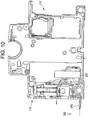
- Fig. 10 is a schematic diagram illustrating a circuit breaker connection arrangement of the circuit breaker 100 in accordance with one embodiment of the present invention.
- a first current path region 250 (as indicated by a dotted line) is provided.
- the first current path region 250 includes a neutral conductor 255 at the second circuit connection portion 115, and a side portion and a center portion of the current transformer 205.
- the current flows between the second circuit connection portion 115 and the side portion and the center portion of the current transformer 205.
- a second current path region 350 (as indicated by a dotted line) is provided.
- the second current path region 350 includes a line conductor 355 at the first circuit connection portion 113, the electromagnetic protection device 306, the thermal protection device 308 and the center portion of the current transformer 205.
- current flows between the first circuit connection portion 113, the electromagnetic protection device 306, the thermal protection device 308, the center portion of the current transformer 205 and the second circuit connection portion 115.
- Fig. 12 is a schematic diagram illustrating a circuit breaker connection arrangement of the circuit breaker 100 in accordance with an alternative embodiment of the present invention.
- a first current path region 260 is provided.
- the first current path region 260 includes a neutral conductor 265 at the first circuit connection portion 113, a side portion of the arc distinguishing device 307 and the center portion of the current transformer 205.
- a second current path region 360 is provided in the first current path region 260.
- the second current path region 360 includes the first circuit connection portion 113, a line conductor 365 at the second circuit connection portion 115, the center portion of the current transformer 205 and the thermal protection device 308. As shown in Fig. 12 , in the second current path region 360, the current flows between the first circuit connection portion 113, the center portion of the current transformer 205, the thermal protection device 308 and the second circuit connection portion 115. As shown in Fig. 6 , the current transformer 205 is aligned adjacent to the trip solenoid 203 according to this embodiment of the present invention.
- Figs. 13 and 14 are schematic diagrams illustrating a circuit breaker connection arrangement of the circuit breaker 100 in accordance with yet another embodiment of the present invention.
- a first current path region 270 (as indicated by the dotted line) is provided.
- the first current path region 270 includes the first circuit connection portion 113, a neutral conductor 275 at the second circuit connection portion 115, the center portion of the current transformer 205 and a side portion of the arc distinguishing device 307.
- current flows between the first circuit connection portion 113, the center portion of the current transformer 205, the side portion of the arc distinguishing device 307 and the second circuit connection portion 115.
- Fig. 13 current flows between the first circuit connection portion 113, the center portion of the current transformer 205, the side portion of the arc distinguishing device 307 and the second circuit connection portion 115.
- a second current path region 370 (as indicated by the dotted line) is provided.
- the second current path region 370 includes a line conductor 375 at the first circuit connection portion 113, the electromagnetic protection device 306, the movable contact arm 304, the thermal protection device 308, the center portion of the current transformer 205 and the second circuit connection portion 115.
- current flows between the first circuit connection portion 113, the electromagnetic protection device 306, the movable contact arm 304, the thermal protection device 308, the center portion of the current transformer 205 and the second circuit connection portion 115.
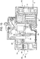
- Fig. 15 is a schematic diagram illustrating a circuit breaker connection arrangement according to yet another embodiment of the present invention.
- a first current path region 280 is provided.
- the first current path region 280 includes the first circuit connection portion 113, a neutral conductor 285 at the second circuit connection portion 115, the center portion of the current transformer 205 and a side portion of the arc distinguishing device 307.
- current flows between the first circuit connection portion 113, the center portion of the current transformer 205, the side of the arc distinguishing device 307 and the second circuit connection portion 115.
- a second current path region 380 is provided in a second current path region 380.
- the second current path region 380 includes the first circuit connection portion 113, a line conductor 385 at the second circuit connection portion 115, the center portion of the current transformer 205, the thermal protection device 308 and the side portion of the arc distinguishing device 307. As shown in Fig. 15 , in the second current path region 380, the current flows between the first circuit connection portion 113, the center portion of the current transformer 205, the thermal protection device 308, the side of the arc distinguishing device 307 and the second circuit connection portion 115.
- Fig. 16 is a diagram illustrating a phase conductor in accordance with an embodiment of the present invention.
- the phase conductor 800 is formed in a U-shape and includes a first end portion 800a and a second end portion 800b, the second end portion 800b further including a surface configured to electrically connect with the electromagnetic device 306.
- Fig 17 is a diagram illustrating the phase conductor shown in Fig. 16 disposed within the circuit breaker 100 in accordance with an embodiment of the present invention.
- the first end portion 800a extends out of the first circuit connection portion 113 and the second end 800b is in power connection with the electromagnetic device 306.
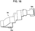
- Fig. 18 is a diagram illustrating a flying neutral conductor of the circuit breaker 100 in accordance with an embodiment of the present invention.
- the flying neutral conductor 900 includes a first end portion 900a and a second end portion 900b.
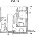
- Fig. 19 is a diagram illustrating the flying neutral conductor 900 shown in Fig. 18 , from the MCB pole side 300 of the circuit breaker 100 in accordance with an embodiment of the present invention.
- the flying neutral conductor 900 is referred to as "flying" since the first end portion 900a extends from the second circuit connection portion 115 and is connected to a neutral bus bar, for example.
- the flying neutral terminal conductor 900 is configured to extend around a side of the current transformer 205 on the MCB pole side 300 and through the center of the current transformer 205 on the RCD side 200 as described below with reference to Fig. 20 .
- Fig. 20 is a diagram illustrating the flying neutral conductor 900 shown in Fig. 19 from the RCD side 200 of the circuit breaker 100 in accordance with an embodiment of the present invention. As shown in Fig. 20 , on the RCD side 200 it can be seen that the second end portion 900b of the flying neutral conductor 900 is connected at the second circuit connection portion 115 of the circuit breaker 100. Further as shown, the flying neutral conductor 900 is disposed through the center of the current transformer 205 on the RCD side 200.
- Fig. 21 is a perspective view of the flying neutral conductor 900 from both the RCD side 200 and the MCB pole side 300 of the circuit breaker 100 in accordance with an embodiment of the present invention.
- the flying neutral conductor 900 is configured to be disposed on the MCB pole side 300 and to extend to the RCD side 200. That is, as shown in Fig. 22, the flying neutral conductor 900 extends from the MCB side 300 to the RCD side 200 within the circuit breaker 100.
- Embodiments of the present invention provide a compact electronic Residual Current Circuit Breaker with Overcurrent Protection (eRCBO) where the PCB of the circuit breaker is installed in substantially half of the single pole module. Further, the PCB is arranged such that a trip solenoid thereof interfaces with a lever mechanism for tripping the MCB mechanism located on an adjacent portion of the circuit breaker. Further, according to an embodiment of the present invention, the circuit breaker connection arrangement includes a flying neutral conductor accommodated in substantially half of the 18 mm module.
- eRCBO Residual Current Circuit Breaker with Overcurrent Protection
Landscapes
- Breakers (AREA)
Claims (8)
- Coupe-circuit (100) comprenant :un module à pôle unique (110) d'un coupe-circuit (100) comprenant une première partie (200) comprenant une première région de trajet de courant (250, 260, 270, 280) et des première et seconde sections (103, 105), et une seconde partie (300) opposée à la première partie (200) comprenant une seconde région de trajet de courant (350, 360, 370, 380) et des première, seconde, troisième et quatrième sections (106, 107, 108, 109), les première et seconde parties (200, 300) étant séparées par une paroi interne (111) ;une carte de circuit (201) comprenant un solénoïde de déclenchement (203) disposé dans la première section (103) de la première partie (200) ;un mécanisme de levier (207) en communication fonctionnelle avec le solénoïde de déclenchement (203) et disposé dans la seconde section (105) de la première partie (200), le mécanisme de levier (207) comprenant en outre une partie d'extrémité conçue pour être en communication fonctionnelle avec le solénoïde de déclenchement (203) et conçue pour être actionnée par le solénoïde de déclenchement (203) lors d'une condition électrique prédéterminée ; etun dispositif de protection de circuit (305) disposé dans les première, seconde, troisième et quatrième sections (106, 107, 108, 109) de la seconde partie (300) et un mécanisme de déclenchement (309) en communication fonctionnelle avec le dispositif de protection de circuit (305) et disposé dans la troisième section (108) de la seconde partie (300), dans lequel le mécanisme de levier (207) est en communication fonctionnelle avec le mécanisme de déclenchement (309) et est conçu pour déclencher le coupe-circuit (100) ;dans lequel les première et seconde sections (103, 105) de la première partie (200) du module à pôle unique (110) occupent essentiellement la moitié du module à pôle unique (110), et les première, seconde, troisième et quatrième sections (106, 107, 108, 109) de la seconde partie (300) du module à pôle unique (110) occupent essentiellement la moitié du module à pôle unique (110) ;dans lequel la seconde section (105) de la première partie (200) et les troisième et quatrième sections (108, 109) de la seconde partie (300) sont disposées en face l'une de l'autre ; caractérisé en ce que :le mécanisme de levier (207) comprend une broche (207a) sur un côté de celui-ci qui s'étend à travers la paroi interne (111), et la troisième section (108) de la seconde partie (300) comprend en outre un activateur (317) en communication fonctionnelle avec la broche (207a) du mécanisme de levier (207) et conçu pour se déplacer lorsque le mécanisme de levier (207) est actionné.
- Coupe-circuit (100) selon la revendication 1, dans lequel le coupe-circuit (100) comprend en outre :un contact fixe (312) et un contact mobile (313), et un bras de contact mobile (304) comprenant le contact mobile (313) sur celui-ci, le bras de contact (304) étant conçu pour séparer le contact mobile (313) du contact fixe (312) lorsque l'activateur (317) se déplace ; etun transformateur de courant (205) conçu pour contrôler le débit de courant.
- Coupe-circuit (100) selon la revendication 2, dans lequel le transformateur de courant (205) est disposé à une extrémité de la carte de circuit (201) opposée à celle du solénoïde de déclenchement (203), le transformateur de courant (205) étant en outre disposé de manière à chevaucher la carte de circuit (201).
- Coupe-circuit (100) selon la revendication 2 ou la revendication 3, dans lequel le transformateur de courant (205) est disposé à proximité du solénoïde de déclenchement (203) dans la carte de circuit (201).
- Coupe-circuit (100) selon l'une quelconque des revendications précédentes, comprenant en outre : un dispositif de protection électromagnétique (306) dans la première section (106) de la seconde partie (300), un dispositif de distinction d'arc (307) dans la seconde section (107) de la seconde partie (300), un dispositif de protection thermique (308) dans la troisième section (108) de la seconde partie (300), et un mécanisme d'actionnement (302) dans la quatrième section (109) de la seconde partie (300).
- Coupe-circuit (100) selon l'une quelconque des revendications précédentes, comprenant en outre : des parties de connexion de circuit (113, 115) disposées à des parties d'extrémité respectives du module à pôle unique (110) et comprenant une première partie de connexion de circuit (113) adjacente au dispositif de protection de circuit (305) et une seconde partie de connexion de circuit (115) adjacente à la carte de circuit (201).
- Coupe-circuit (100) selon l'une quelconque des revendications précédentes, dans lequel la première partie de connexion de circuit (113) comprend une partie ouverte (114a) et le coupe-circuit (100) comprend en outre un conducteur de phase (800) disposé dans la partie ouverte (114a) et ayant une forme de U, le conducteur de phase (800) comprenant une première partie d'extrémité (800a) et une seconde partie d'extrémité (800b), la seconde partie d'extrémité (800b) comprenant une surface conçue pour se connecter électriquement au dispositif de protection électromagnétique (306).
- Coupe-circuit (100) selon l'une quelconque des revendications précédentes, dans lequel le coupe-circuit (100) comprend en outre un conducteur neutre volant (900) disposé dans la seconde partie de connexion de circuit (115) et comprenant une première partie d'extrémité (900a) s'étendant depuis la seconde partie de connexion de circuit (115) et autour d'un côté du transformateur de courant (205) et à travers un centre du transformateur de courant (205), et la seconde partie d'extrémité (900b) disposée au niveau de la seconde partie de connexion de circuit (115).
Applications Claiming Priority (1)
| Application Number | Priority Date | Filing Date | Title |
|---|---|---|---|
| US12/426,248 US7994882B2 (en) | 2009-04-18 | 2009-04-18 | Space allocation within a circuit breaker |
Publications (3)
| Publication Number | Publication Date |
|---|---|
| EP2242077A2 EP2242077A2 (fr) | 2010-10-20 |
| EP2242077A3 EP2242077A3 (fr) | 2013-10-30 |
| EP2242077B1 true EP2242077B1 (fr) | 2017-08-09 |
Family
ID=42246311
Family Applications (1)
| Application Number | Title | Priority Date | Filing Date |
|---|---|---|---|
| EP10160205.0A Active EP2242077B1 (fr) | 2009-04-18 | 2010-04-16 | Attribution d'espace dans un disjoncteur |
Country Status (3)
| Country | Link |
|---|---|
| US (1) | US7994882B2 (fr) |
| EP (1) | EP2242077B1 (fr) |
| CN (1) | CN101923989B (fr) |
Families Citing this family (10)
| Publication number | Priority date | Publication date | Assignee | Title |
|---|---|---|---|---|
| US9349559B2 (en) * | 2009-03-23 | 2016-05-24 | Siemens Industry, Inc. | Low-profile electronic circuit breakers, breaker tripping mechanisms, and systems and methods of using same |
| US20120250206A1 (en) * | 2011-03-30 | 2012-10-04 | General Electric Company | Compact residual current breaker with overcurrent protection |
| CN102254757B (zh) * | 2011-06-24 | 2013-08-14 | 人民电器集团有限公司 | 一种小型断路器的中性极结构 |
| US9899160B2 (en) * | 2013-08-19 | 2018-02-20 | Siemens Industry, Inc. | Low-profile electronic circuit breakers, systems, and methods |
| WO2015047820A1 (fr) * | 2013-09-26 | 2015-04-02 | Labinal, Llc | Module de disjoncteur avec disjoncteurs enfichables |
| CN106710972B (zh) * | 2015-07-16 | 2018-11-02 | 上海良信电器股份有限公司 | 断路器 |
| CN106206183B (zh) * | 2016-08-29 | 2019-01-01 | 苏州未来电器股份有限公司 | 一种n相断路器单元及断路器壳体 |
| CN108400066B (zh) * | 2017-02-04 | 2020-04-21 | 西门子公司 | 单级断路器 |
| CN108695115B (zh) * | 2017-04-06 | 2020-05-26 | 西门子公司 | 剩余电流动作断路器 |
| US10852326B2 (en) * | 2017-08-09 | 2020-12-01 | Schneider Electric USA, Inc. | Differential current sensing bussing method |
Family Cites Families (9)
| Publication number | Priority date | Publication date | Assignee | Title |
|---|---|---|---|---|
| US5089796A (en) * | 1990-09-19 | 1992-02-18 | Square D Company | Earth leakage trip indicator |
| NO304860B1 (no) * | 1991-07-22 | 1999-02-22 | Pdl Holdings Ltd | Brytermekanisme |
| US5517165A (en) * | 1991-07-22 | 1996-05-14 | Pdl Holdings Limited | Switch mechanism |
| US5510759A (en) | 1994-06-23 | 1996-04-23 | Eaton Corporation | Miniature circuit breaker with ground fault electronics supported by stiff conductors for easy assembly |
| US5907461A (en) * | 1997-10-01 | 1999-05-25 | Eaton Corporation | Molded case circuit breaker with ground fault protection and signaling switches |
| US6259340B1 (en) * | 1999-05-10 | 2001-07-10 | General Electric Company | Circuit breaker with a dual test button mechanism |
| US6487057B1 (en) * | 2000-06-13 | 2002-11-26 | Eaton Corporation | Ground fault current interrupter/arc fault current interrupter circuit breaker with fail safe mechanism |
| WO2002080328A1 (fr) | 2001-03-30 | 2002-10-10 | Pdl Holdings Limited | Dispositif de circuit electrique a configuration compacte de bornes |
| US7170376B2 (en) | 2004-12-09 | 2007-01-30 | Eaton Corporation | Electrical switching apparatus including a housing and a trip circuit forming a composite structure |
-
2009
- 2009-04-18 US US12/426,248 patent/US7994882B2/en active Active
-
2010
- 2010-04-16 EP EP10160205.0A patent/EP2242077B1/fr active Active
- 2010-04-16 CN CN201010167744.4A patent/CN101923989B/zh active Active
Non-Patent Citations (1)
| Title |
|---|
| None * |
Also Published As
| Publication number | Publication date |
|---|---|
| EP2242077A2 (fr) | 2010-10-20 |
| AU2010201536A1 (en) | 2010-11-04 |
| US7994882B2 (en) | 2011-08-09 |
| EP2242077A3 (fr) | 2013-10-30 |
| US20100264000A1 (en) | 2010-10-21 |
| CN101923989A (zh) | 2010-12-22 |
| CN101923989B (zh) | 2014-01-22 |
Similar Documents
| Publication | Publication Date | Title |
|---|---|---|
| EP2242077B1 (fr) | Attribution d'espace dans un disjoncteur | |
| US4281359A (en) | Static trip unit for molded case circuit breakers | |
| US6624375B2 (en) | Wire lug/arc vent barrier molded case circuit breaker | |
| EP1939912B1 (fr) | Activation pour appareil de commutation | |
| US7843291B2 (en) | Integrated maglatch accessory | |
| US6750743B1 (en) | Integrated thermal and magnetic trip unit | |
| CN101689446A (zh) | 电气安装配电电器 | |
| CA2966097C (fr) | Disjoncteur modulaire et methode d'assemblage | |
| JPH0821307B2 (ja) | 回路遮断器 | |
| US9852851B2 (en) | Molded case circuit breaker with current sensing unit | |
| EP2242080B1 (fr) | Ensemble de test pour disjoncteur | |
| JP4325749B2 (ja) | 異なるフレーム・サイズ用のモジュラ接触システムを備えた回路遮断器 | |
| EP3382731B1 (fr) | Disjoncteurs | |
| EP2506283B1 (fr) | Disjoncteur de courant résiduel compact avec protection contre les surintensités | |
| EP0255955B1 (fr) | Coupe-circuit | |
| US6274833B1 (en) | Plug-in trip unit joint for a molded case circuit breaker | |
| CN104115249B (zh) | 包括凸轮杆的电接触设备、断路器和电接触组件及操作方法 | |
| US9053888B2 (en) | Tie bar for molded case circuit breaker and method of assembly | |
| CN202871718U (zh) | 电路中断装置和用于与断路器一起使用的脱扣机构 | |
| JP5517566B2 (ja) | 漏電遮断器 | |
| EP1414057A1 (fr) | Disjoncteur a air | |
| CN100386837C (zh) | 用于断路器的改进的联锁机构及装有该联锁机构的断路器 | |
| GB2071915A (en) | Static trip unit and interlock for circuit breaker | |
| JP4499890B2 (ja) | 回路遮断器 | |
| US5886599A (en) | Molded case circuit breaker having an improved electromagnetic trip |
Legal Events
| Date | Code | Title | Description |
|---|---|---|---|
| PUAI | Public reference made under article 153(3) epc to a published international application that has entered the european phase |
Free format text: ORIGINAL CODE: 0009012 |
|
| AK | Designated contracting states |
Kind code of ref document: A2 Designated state(s): AT BE BG CH CY CZ DE DK EE ES FI FR GB GR HR HU IE IS IT LI LT LU LV MC MK MT NL NO PL PT RO SE SI SK SM TR |
|
| AX | Request for extension of the european patent |
Extension state: AL BA ME RS |
|
| PUAL | Search report despatched |
Free format text: ORIGINAL CODE: 0009013 |
|
| AK | Designated contracting states |
Kind code of ref document: A3 Designated state(s): AT BE BG CH CY CZ DE DK EE ES FI FR GB GR HR HU IE IS IT LI LT LU LV MC MK MT NL NO PL PT RO SE SI SK SM TR |
|
| AX | Request for extension of the european patent |
Extension state: AL BA ME RS |
|
| RIC1 | Information provided on ipc code assigned before grant |
Ipc: H01H 83/22 20060101ALN20130926BHEP Ipc: H01H 83/20 20060101ALI20130926BHEP Ipc: H01H 71/02 20060101AFI20130926BHEP |
|
| 17P | Request for examination filed |
Effective date: 20140430 |
|
| RBV | Designated contracting states (corrected) |
Designated state(s): AT BE BG CH CY CZ DE DK EE ES FI FR GB GR HR HU IE IS IT LI LT LU LV MC MK MT NL NO PL PT RO SE SI SK SM TR |
|
| GRAP | Despatch of communication of intention to grant a patent |
Free format text: ORIGINAL CODE: EPIDOSNIGR1 |
|
| RIC1 | Information provided on ipc code assigned before grant |
Ipc: H01H 83/20 20060101ALI20170322BHEP Ipc: H01H 83/22 20060101ALN20170322BHEP Ipc: H01H 71/02 20060101AFI20170322BHEP |
|
| INTG | Intention to grant announced |
Effective date: 20170406 |
|
| GRAS | Grant fee paid |
Free format text: ORIGINAL CODE: EPIDOSNIGR3 |
|
| GRAA | (expected) grant |
Free format text: ORIGINAL CODE: 0009210 |
|
| AK | Designated contracting states |
Kind code of ref document: B1 Designated state(s): AT BE BG CH CY CZ DE DK EE ES FI FR GB GR HR HU IE IS IT LI LT LU LV MC MK MT NL NO PL PT RO SE SI SK SM TR |
|
| REG | Reference to a national code |
Ref country code: GB Ref legal event code: FG4D |
|
| REG | Reference to a national code |
Ref country code: CH Ref legal event code: EP Ref country code: AT Ref legal event code: REF Ref document number: 917664 Country of ref document: AT Kind code of ref document: T Effective date: 20170815 |
|
| REG | Reference to a national code |
Ref country code: IE Ref legal event code: FG4D |
|
| REG | Reference to a national code |
Ref country code: DE Ref legal event code: R096 Ref document number: 602010044201 Country of ref document: DE |
|
| REG | Reference to a national code |
Ref country code: NL Ref legal event code: MP Effective date: 20170809 |
|
| REG | Reference to a national code |
Ref country code: LT Ref legal event code: MG4D |
|
| REG | Reference to a national code |
Ref country code: AT Ref legal event code: MK05 Ref document number: 917664 Country of ref document: AT Kind code of ref document: T Effective date: 20170809 |
|
| PG25 | Lapsed in a contracting state [announced via postgrant information from national office to epo] |
Ref country code: LT Free format text: LAPSE BECAUSE OF FAILURE TO SUBMIT A TRANSLATION OF THE DESCRIPTION OR TO PAY THE FEE WITHIN THE PRESCRIBED TIME-LIMIT Effective date: 20170809 Ref country code: FI Free format text: LAPSE BECAUSE OF FAILURE TO SUBMIT A TRANSLATION OF THE DESCRIPTION OR TO PAY THE FEE WITHIN THE PRESCRIBED TIME-LIMIT Effective date: 20170809 Ref country code: NO Free format text: LAPSE BECAUSE OF FAILURE TO SUBMIT A TRANSLATION OF THE DESCRIPTION OR TO PAY THE FEE WITHIN THE PRESCRIBED TIME-LIMIT Effective date: 20171109 Ref country code: HR Free format text: LAPSE BECAUSE OF FAILURE TO SUBMIT A TRANSLATION OF THE DESCRIPTION OR TO PAY THE FEE WITHIN THE PRESCRIBED TIME-LIMIT Effective date: 20170809 Ref country code: NL Free format text: LAPSE BECAUSE OF FAILURE TO SUBMIT A TRANSLATION OF THE DESCRIPTION OR TO PAY THE FEE WITHIN THE PRESCRIBED TIME-LIMIT Effective date: 20170809 Ref country code: AT Free format text: LAPSE BECAUSE OF FAILURE TO SUBMIT A TRANSLATION OF THE DESCRIPTION OR TO PAY THE FEE WITHIN THE PRESCRIBED TIME-LIMIT Effective date: 20170809 Ref country code: SE Free format text: LAPSE BECAUSE OF FAILURE TO SUBMIT A TRANSLATION OF THE DESCRIPTION OR TO PAY THE FEE WITHIN THE PRESCRIBED TIME-LIMIT Effective date: 20170809 |
|
| PG25 | Lapsed in a contracting state [announced via postgrant information from national office to epo] |
Ref country code: GR Free format text: LAPSE BECAUSE OF FAILURE TO SUBMIT A TRANSLATION OF THE DESCRIPTION OR TO PAY THE FEE WITHIN THE PRESCRIBED TIME-LIMIT Effective date: 20171110 Ref country code: BG Free format text: LAPSE BECAUSE OF FAILURE TO SUBMIT A TRANSLATION OF THE DESCRIPTION OR TO PAY THE FEE WITHIN THE PRESCRIBED TIME-LIMIT Effective date: 20171109 Ref country code: IS Free format text: LAPSE BECAUSE OF FAILURE TO SUBMIT A TRANSLATION OF THE DESCRIPTION OR TO PAY THE FEE WITHIN THE PRESCRIBED TIME-LIMIT Effective date: 20171209 Ref country code: PL Free format text: LAPSE BECAUSE OF FAILURE TO SUBMIT A TRANSLATION OF THE DESCRIPTION OR TO PAY THE FEE WITHIN THE PRESCRIBED TIME-LIMIT Effective date: 20170809 Ref country code: ES Free format text: LAPSE BECAUSE OF FAILURE TO SUBMIT A TRANSLATION OF THE DESCRIPTION OR TO PAY THE FEE WITHIN THE PRESCRIBED TIME-LIMIT Effective date: 20170809 Ref country code: LV Free format text: LAPSE BECAUSE OF FAILURE TO SUBMIT A TRANSLATION OF THE DESCRIPTION OR TO PAY THE FEE WITHIN THE PRESCRIBED TIME-LIMIT Effective date: 20170809 |
|
| REG | Reference to a national code |
Ref country code: FR Ref legal event code: PLFP Year of fee payment: 9 |
|
| PG25 | Lapsed in a contracting state [announced via postgrant information from national office to epo] |
Ref country code: DK Free format text: LAPSE BECAUSE OF FAILURE TO SUBMIT A TRANSLATION OF THE DESCRIPTION OR TO PAY THE FEE WITHIN THE PRESCRIBED TIME-LIMIT Effective date: 20170809 Ref country code: CZ Free format text: LAPSE BECAUSE OF FAILURE TO SUBMIT A TRANSLATION OF THE DESCRIPTION OR TO PAY THE FEE WITHIN THE PRESCRIBED TIME-LIMIT Effective date: 20170809 Ref country code: RO Free format text: LAPSE BECAUSE OF FAILURE TO SUBMIT A TRANSLATION OF THE DESCRIPTION OR TO PAY THE FEE WITHIN THE PRESCRIBED TIME-LIMIT Effective date: 20170809 |
|
| REG | Reference to a national code |
Ref country code: DE Ref legal event code: R097 Ref document number: 602010044201 Country of ref document: DE |
|
| PG25 | Lapsed in a contracting state [announced via postgrant information from national office to epo] |
Ref country code: SM Free format text: LAPSE BECAUSE OF FAILURE TO SUBMIT A TRANSLATION OF THE DESCRIPTION OR TO PAY THE FEE WITHIN THE PRESCRIBED TIME-LIMIT Effective date: 20170809 Ref country code: EE Free format text: LAPSE BECAUSE OF FAILURE TO SUBMIT A TRANSLATION OF THE DESCRIPTION OR TO PAY THE FEE WITHIN THE PRESCRIBED TIME-LIMIT Effective date: 20170809 Ref country code: SK Free format text: LAPSE BECAUSE OF FAILURE TO SUBMIT A TRANSLATION OF THE DESCRIPTION OR TO PAY THE FEE WITHIN THE PRESCRIBED TIME-LIMIT Effective date: 20170809 Ref country code: IT Free format text: LAPSE BECAUSE OF FAILURE TO SUBMIT A TRANSLATION OF THE DESCRIPTION OR TO PAY THE FEE WITHIN THE PRESCRIBED TIME-LIMIT Effective date: 20170809 |
|
| PLBE | No opposition filed within time limit |
Free format text: ORIGINAL CODE: 0009261 |
|
| STAA | Information on the status of an ep patent application or granted ep patent |
Free format text: STATUS: NO OPPOSITION FILED WITHIN TIME LIMIT |
|
| 26N | No opposition filed |
Effective date: 20180511 |
|
| PG25 | Lapsed in a contracting state [announced via postgrant information from national office to epo] |
Ref country code: SI Free format text: LAPSE BECAUSE OF FAILURE TO SUBMIT A TRANSLATION OF THE DESCRIPTION OR TO PAY THE FEE WITHIN THE PRESCRIBED TIME-LIMIT Effective date: 20170809 |
|
| PG25 | Lapsed in a contracting state [announced via postgrant information from national office to epo] |
Ref country code: MC Free format text: LAPSE BECAUSE OF FAILURE TO SUBMIT A TRANSLATION OF THE DESCRIPTION OR TO PAY THE FEE WITHIN THE PRESCRIBED TIME-LIMIT Effective date: 20170809 |
|
| REG | Reference to a national code |
Ref country code: CH Ref legal event code: PL |
|
| REG | Reference to a national code |
Ref country code: BE Ref legal event code: MM Effective date: 20180430 |
|
| GBPC | Gb: european patent ceased through non-payment of renewal fee |
Effective date: 20180416 |
|
| REG | Reference to a national code |
Ref country code: IE Ref legal event code: MM4A |
|
| PG25 | Lapsed in a contracting state [announced via postgrant information from national office to epo] |
Ref country code: LU Free format text: LAPSE BECAUSE OF NON-PAYMENT OF DUE FEES Effective date: 20180416 |
|
| PG25 | Lapsed in a contracting state [announced via postgrant information from national office to epo] |
Ref country code: LI Free format text: LAPSE BECAUSE OF NON-PAYMENT OF DUE FEES Effective date: 20180430 Ref country code: CH Free format text: LAPSE BECAUSE OF NON-PAYMENT OF DUE FEES Effective date: 20180430 Ref country code: GB Free format text: LAPSE BECAUSE OF NON-PAYMENT OF DUE FEES Effective date: 20180416 Ref country code: BE Free format text: LAPSE BECAUSE OF NON-PAYMENT OF DUE FEES Effective date: 20180430 |
|
| PG25 | Lapsed in a contracting state [announced via postgrant information from national office to epo] |
Ref country code: IE Free format text: LAPSE BECAUSE OF NON-PAYMENT OF DUE FEES Effective date: 20180416 |
|
| PG25 | Lapsed in a contracting state [announced via postgrant information from national office to epo] |
Ref country code: MT Free format text: LAPSE BECAUSE OF NON-PAYMENT OF DUE FEES Effective date: 20180416 |
|
| PG25 | Lapsed in a contracting state [announced via postgrant information from national office to epo] |
Ref country code: TR Free format text: LAPSE BECAUSE OF FAILURE TO SUBMIT A TRANSLATION OF THE DESCRIPTION OR TO PAY THE FEE WITHIN THE PRESCRIBED TIME-LIMIT Effective date: 20170809 |
|
| PG25 | Lapsed in a contracting state [announced via postgrant information from national office to epo] |
Ref country code: HU Free format text: LAPSE BECAUSE OF FAILURE TO SUBMIT A TRANSLATION OF THE DESCRIPTION OR TO PAY THE FEE WITHIN THE PRESCRIBED TIME-LIMIT; INVALID AB INITIO Effective date: 20100416 Ref country code: PT Free format text: LAPSE BECAUSE OF FAILURE TO SUBMIT A TRANSLATION OF THE DESCRIPTION OR TO PAY THE FEE WITHIN THE PRESCRIBED TIME-LIMIT Effective date: 20170809 |
|
| PG25 | Lapsed in a contracting state [announced via postgrant information from national office to epo] |
Ref country code: CY Free format text: LAPSE BECAUSE OF FAILURE TO SUBMIT A TRANSLATION OF THE DESCRIPTION OR TO PAY THE FEE WITHIN THE PRESCRIBED TIME-LIMIT Effective date: 20170809 Ref country code: MK Free format text: LAPSE BECAUSE OF NON-PAYMENT OF DUE FEES Effective date: 20170809 |
|
| REG | Reference to a national code |
Ref country code: DE Ref legal event code: R081 Ref document number: 602010044201 Country of ref document: DE Owner name: ABB SCHWEIZ AG, CH Free format text: FORMER OWNER: GENERAL ELECTRIC COMPANY, SCHENECTADY, N.Y., US Ref country code: DE Ref legal event code: R081 Ref document number: 602010044201 Country of ref document: DE Owner name: ABB SCHWEIZ AG, CH Free format text: FORMER OWNER: GENERAL ELECTRIC COMPANY, SCHENECTADY, NY, US |
|
| PGFP | Annual fee paid to national office [announced via postgrant information from national office to epo] |
Ref country code: DE Payment date: 20250422 Year of fee payment: 16 |
|
| REG | Reference to a national code |
Ref country code: DE Ref legal event code: R082 Ref document number: 602010044201 Country of ref document: DE Representative=s name: ZIMMERMANN & PARTNER PATENTANWAELTE MBB, DE |
|
| PGFP | Annual fee paid to national office [announced via postgrant information from national office to epo] |
Ref country code: FR Payment date: 20250424 Year of fee payment: 16 |