EP2242256A1 - Festkörper-bildgeberbauelement und verfahren zu seiner herstellung - Google Patents
Festkörper-bildgeberbauelement und verfahren zu seiner herstellung Download PDFInfo
- Publication number
- EP2242256A1 EP2242256A1 EP09707681A EP09707681A EP2242256A1 EP 2242256 A1 EP2242256 A1 EP 2242256A1 EP 09707681 A EP09707681 A EP 09707681A EP 09707681 A EP09707681 A EP 09707681A EP 2242256 A1 EP2242256 A1 EP 2242256A1
- Authority
- EP
- European Patent Office
- Prior art keywords
- state imaging
- solid state
- imaging device
- imaging element
- board
- Prior art date
- Legal status (The legal status is an assumption and is not a legal conclusion. Google has not performed a legal analysis and makes no representation as to the accuracy of the status listed.)
- Withdrawn
Links
Images


Classifications
-
- H—ELECTRICITY
- H10—SEMICONDUCTOR DEVICES; ELECTRIC SOLID-STATE DEVICES NOT OTHERWISE PROVIDED FOR
- H10F—INORGANIC SEMICONDUCTOR DEVICES SENSITIVE TO INFRARED RADIATION, LIGHT, ELECTROMAGNETIC RADIATION OF SHORTER WAVELENGTH OR CORPUSCULAR RADIATION
- H10F39/00—Integrated devices, or assemblies of multiple devices, comprising at least one element covered by group H10F30/00, e.g. radiation detectors comprising photodiode arrays
- H10F39/80—Constructional details of image sensors
- H10F39/804—Containers or encapsulations
-
- H—ELECTRICITY
- H04—ELECTRIC COMMUNICATION TECHNIQUE
- H04N—PICTORIAL COMMUNICATION, e.g. TELEVISION
- H04N23/00—Cameras or camera modules comprising electronic image sensors; Control thereof
- H04N23/50—Constructional details
- H04N23/54—Mounting of pick-up tubes, electronic image sensors, deviation or focusing coils
-
- H—ELECTRICITY
- H04—ELECTRIC COMMUNICATION TECHNIQUE
- H04N—PICTORIAL COMMUNICATION, e.g. TELEVISION
- H04N23/00—Cameras or camera modules comprising electronic image sensors; Control thereof
- H04N23/57—Mechanical or electrical details of cameras or camera modules specially adapted for being embedded in other devices
-
- H—ELECTRICITY
- H10—SEMICONDUCTOR DEVICES; ELECTRIC SOLID-STATE DEVICES NOT OTHERWISE PROVIDED FOR
- H10F—INORGANIC SEMICONDUCTOR DEVICES SENSITIVE TO INFRARED RADIATION, LIGHT, ELECTROMAGNETIC RADIATION OF SHORTER WAVELENGTH OR CORPUSCULAR RADIATION
- H10F39/00—Integrated devices, or assemblies of multiple devices, comprising at least one element covered by group H10F30/00, e.g. radiation detectors comprising photodiode arrays
- H10F39/80—Constructional details of image sensors
- H10F39/806—Optical elements or arrangements associated with the image sensors
- H10F39/8063—Microlenses
-
- H—ELECTRICITY
- H10—SEMICONDUCTOR DEVICES; ELECTRIC SOLID-STATE DEVICES NOT OTHERWISE PROVIDED FOR
- H10W—GENERIC PACKAGES, INTERCONNECTIONS, CONNECTORS OR OTHER CONSTRUCTIONAL DETAILS OF DEVICES COVERED BY CLASS H10
- H10W74/00—Encapsulations, e.g. protective coatings
- H10W74/10—Encapsulations, e.g. protective coatings characterised by their shape or disposition
- H10W74/15—Encapsulations, e.g. protective coatings characterised by their shape or disposition on active surfaces of flip-chip devices, e.g. underfills
Definitions
- the present invention relates to a solid state imaging device and a manufacturing method thereof, and more particularly to a small solid state imaging device using a solid state imaging element, such as a monitoring camera, a medical camera, a vehicle-mounted camera, and a camera for use in an information communication terminal and to a method for manufacturing the solid state imaging device.
- a solid state imaging element such as a monitoring camera, a medical camera, a vehicle-mounted camera, and a camera for use in an information communication terminal and to a method for manufacturing the solid state imaging device.
- a mounting structure implemented by such a combination is made by mounting elements on a flat-plate-shaped printed board.
- a demand for slimming down individual devices is growing year by year.
- an attempt is made to further slim down the imaging device by use of a flexible wiring board or by mounting an IC directly on a light-transmitting member though a flip-chip mounting process.
- Patent Document 1 discloses a structure in which a light-transmitting member and a photoelectric conversion element are disposed opposite each other across a flexible wiring board.
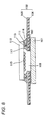
- Fig. 8 shows the photoelectric conversion element described in connection with Patent Document 1.
- a light-transmitting member 101 is bonded to a flexible wiring board 102 via an adhesive 103.
- a metal wiring pattern 105 is laid on a resin film 104, and an opening 106 is formed therein.
- the light-transmitting member 101 and an imaging element 112 are disposed opposite each other across the opening 106.
- Bumps 113 are provided on an electrode pad 117 of the solid state imaging element 112 including microlenses 115 formed in an imaging area of the imaging element 112.
- the bumps 113 are electrically connected to the metal wiring pattern 105 of the flexible board 102 via an anisotropic conductive film 111. Further, bonding strength of the solid state imaging element 112 is further reinforced by a sealing resin 116.
- Patent Document 2 discloses a method for dissipating heat of a solid state imaging device as countermeasures against the faulty operation and the influence.
- a Peltier element cools a heated solid state imaging element, and heat is dissipated through a heat sink disposed opposite to the solid state imaging element.
- Patent Document 2 When the method described in Patent Document 2 is applied to the solid state imaging device, it is necessary to attach the Peltier element and to join the Peltier element to the casing by a meandering heat conduction member. Further, it is necessary to provide power wirings, etc., used for driving the Peltier element. Consequently, there is a problem of an increase in the size and the cost of the imaging device.
- the present invention was made in view of the above-described circumstance, and an object thereof is to provide a slim, highly-reliable solid state imaging device capable of efficiently dissipating heat.
- a solid state imaging device of the present invention is characterized in that a resin mold having a surface of an uneven shape is formed on a rear surface of a solid state imaging element flip-chip mounted to a substrate having an opening portion. According to the configuration, since an area contacting air becomes greater, heat developing from the solid state imaging element can effectively be discharged, which can prevent error caused when the solid state imaging element is raised to high temperature. Since the solid state imaging device has a simple structure for dissipating heat from the rear surface of the solid state imaging element, the solid state imaging device can easily be slimmed down and have high rigidity. Consequently, it is possible to provide a superior solid state imaging device that enables a reduction of size of a portable phone, etc.
- the resin mold in the solid state imaging device, includes a portion where a distance between an outer surface and the solid state imaging element is large and a portion where the distance is small, thereby having a radiator fin function.
- the present invention includes the solid state imaging device in which the uneven shape includes a strip pattern.
- the heat of the solid state imaging element is efficiently dissipated into the outside air by the outside air forming a laminar flow by grooves of the strip pattern.
- the present invention includes the solid state imaging device in which the uneven shape defines a plurality of pillar-shaped projections.
- the configuration can increase the surface area of the outer surface of the resin mold, and also increase the area contacting the outside air, whereby heat of the solid state imaging element is efficiently dissipated into the outside air.
- the present invention includes the solid state imaging device in which the uneven shape includes a lattice pattern.
- the configuration can increase the surface area of the outer surface of the resin mold and also increase the area contacting the outside air becomes. Further, grooves penetrating into side surfaces are formed in the lattice pattern along an outer wall of the uneven surface formed in the lattice pattern. Consequently, a laminar flow is efficiently generated, and heat of the solid state imaging element is efficiently dissipated to the outside.
- the present invention is characterized by comprising: a multilayer board including a flexible wiring board having an opening portion (hereinafter called a "flexible wiring board") and a reinforcing plate integrally stacked on the flexible wiring board; a light-transmitting member placed on a reinforcing plate side of the multilayer board so as to close the opening portion; and a solid state imaging element board placed on a flexible wiring board side of the multilayer board, wherein the reinforcing plate has a reference hole used for setting the solid state imaging element board, and wherein the reinforcing plate is exposed from the flexible wiring board around a peripheral edge of the reference hole, and the solid state imaging element board and the light-transmitting member are placed on both sides of the multilayer board while the reference hole is taken as a common reference.
- a multilayer board including a flexible wiring board having an opening portion (hereinafter called a "flexible wiring board") and a reinforcing plate integrally stacked on the flexible wiring board; a light-transmitting member placed on
- the solid state imaging device has advantages in which high rigidity can be provided even when having a small thickness, strength for the solid state imaging element can also be assured, and the optical axes can be aligned with high precision.
- the flexible board and the reinforcing plate have the same outer shape and dimension and form a multilayer structure.
- the reinforcing plate has the reference hole used when the solid state imaging element board and the light-transmitting member (or an optical lens) are mounted. A surface of the reinforcing plate is exposed from the flexible wiring board side around the reference hole.
- the solid state imaging element board and the light-transmitting member can be placed by commonly using the reference hole from both front side and back side thereof. Therefore, the solid state imaging device can be easily slimmed down and assembled with superior operability.
- solid state imaging element board means a board produced by forming a solid state imaging element on a semiconductor board, such as a silicon board, principally, an individually divided chip.
- the reference hole may include a so-called cut portion partially communicating the outside, as well as a so-called positioning hole in which an outer edge thereof is surrounded by a wall. Further, a wiring pattern, an outer profile, etc., taking the reference hole as a reference may also be indirectly used for positioning.
- the present invention includes the solid state imaging device in which the light-transmitting member and an optical lens are attached to the reinforcing plate, and the optical lens and the solid state imaging element board are positioned while the reference hole is taken as a common reference from both front side and back side thereof. Moreover, it is also preferable that the light-transmitting member is positioned while the reference hole is taken as a common reference.
- the light-transmitting member used in the solid state imaging device of the present invention may be an optical filter. As a result, an infrared region of light entering the solid state imaging element is cut, so that a superior imaging characteristic can be acquired.
- the reinforcing plate used in the solid state imaging device of the present invention may also be a metal plate. As a result, high rigidity for the solid state imaging device can be obtained.
- a ground portion of a wiring pattern of the flexible wiring board used in the solid state imaging device of the present invention and the reinforcing plate made of a metal plate may be electrically connected together. Consequently, a stable electric characteristic can be yielded.
- a periphery of the opening portion of the reinforcing plate where the light-transmitting member used in the solid state imaging device of the present invention is to be placed may be smaller in thickness than a surrounding of the opening portion.
- a chip component may be mounted on the flexible wiring board used in the solid state imaging device of the present invention.
- the degree of design freedom of electric wiring is increased, and chip components can be placed in the vicinity of the solid state imaging element, so that the electric characteristics can be optimized.
- the present invention includes the solid state imaging device in which the resin mold is made of a high thermal conductive material.
- the configuration enables efficient dissipation of heat of the solid state imaging element into the atmosphere.
- the present invention includes: a step of mounting a solid state imaging element on a flexible wiring board having an opening portion though a flip-chip mounting process; a step of filling a rear surface of the solid state imaging element with molding resin; and a step of forming an uneven shape through a transfer using a stamper having a predetermined uneven shape after the step of filling, and hardening the resin with the uneven shape.
- the present invention also includes: a step of mounting a solid state imaging element on the flexible wiring board having an opening portion through a flip-chip mounting process; and a step of forming a resin sealed portion by injection molding using a metal mold having an uneven shape. According to the configuration, it is possible to form an uneven shape with a higher degree of freedom than that provided by the stamper, so that heat radiation can be made more effective.
- the present invention also includes: a step of mounting a solid state imaging element on a flexible wiring board having an opening portion through a flip-chip mounting process; and a step of forming a resin sealed portion by means of a hot melting technique using a metal molding having an uneven shape. According to the configuration, it is possible to manufacture the solid state imaging device with a simpler facility and within a shorter period of time, so that manufacturing cost can be reduced.
- the present invention can slim down a solid state imaging device and can readily provide a highly reliable solid state imaging device exhibiting high rigidity and enhanced accuracy. As a consequence, a portable terminal device can also be slimmed down.
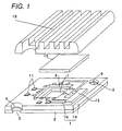
- Fig. 1 is an exploded oblique perspective view of a solid state imaging device of a first embodiment.
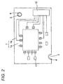
- Fig. 2 is a top view of a flexible wiring board used in the solid state imaging device of the first embodiment.
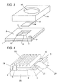
- Fig. 3 is an exploded oblique perspective view of the solid state imaging device of the first embodiment acquired when viewed from behind.
- Fig. 4 is an oblique perspective view of the solid state imaging device of the present invention.
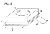
- Fig. 5 is an oblique perspective view of the solid state imaging device of the present invention.
- Fig. 6 is a view showing a result of a radiation effect resultant from simulation of a thermal fluid.
- a resin mold 18 having a surface of an uneven shape is formed on a rear surface of a solid state imaging element board 10 which is mounted to the flexible wiring board 1 having an opening portion 7 through a flip-chip mounting process.
- the resin mold 18 can readily be made by, after coating a rear surface of the solid state imaging element with molding resin, forming the uneven shape at the coated rear surface by transfer using a stamper having an uneven, strip shape, and thereafter heating and hardening the resin.
- the solid state imaging device includes: a multilayer board including the flexible wiring board 1 having the opening portion 7 and a reinforcing plate 2 on which the flexible wiring board 1 is integrally stacked; a light-transmitting member 14 and an optical lens 15 disposed on the reinforcing plate 2 side of the multilayer board so as to close the opening portion 7; and the solid state imaging element board 10 disposed on the flexible wiring board 1 side of the multilayer board.
- the reinforcing plate 2 includes a cut portion 3 and a positioning reference hole 5 that serve as reference holes for setting the solid state imaging element board. The reinforcing plate 2 is exposed to the flexible wiring board 1 around peripheral edges of the cut portion 3 and the positioning hole 5. While taking the two reference holes as common references, the solid state imaging element board, the light-transmitting member 14 and an optical lens 15 (a lens casing 16) are provided on both sides of the multilayer board.
- the flexible wiring board 1 and the reinforcing plate 2 having an outer shape and size identical with those of the flexible wiring board 1 are layered and bonded so as to be integrated together.
- a polyimide resin film having a thickness of 25 ⁇ m is used as a film substrate (a base film) 1 a, and a SUS plate having a thickness of 200 ⁇ m is used for the reinforcing plate 2.
- the cut portion 3 serving as the reference hole is opened in the reinforcing plate 2, and an exposed portion 4 of the reinforcing plate is formed around the cut portion 3.
- the positioning hole 5 serving a reference hole is provided, and an exposed portion 6 of the reinforcing plate 2 is formed around the positioning hole 5.
- the cut portion 3 and the positioning hole 5 that serve as the reference holes can be recognized from both front side and back side as reference shapes formed by the reinforcing plate 2.
- the opening portion 7 is provided, and an exposed portion 8 of the reinforcing plate 2 is formed around the opening portion 7.
- a metal wiring pattern 1 b is formed on the film substrate 1 a in the flexible wiring board 1 and is arranged such that the solid state imaging element board 10 is electrically connected to the metal wiring pattern 1 b.
- chip components 11 and a connector 12 are provided so as to be connected to the metal wiring pattern 1b.
- Ground portions of the metal wiring pattern 1 b are electrically connected to the reinforcing plate 2 of the SUS plate.
- the solid state imaging element board 10 uses a board in which the rear surface thereof is coated with a black epoxy resin film (not shown) serving as a light-shielding film.
- the light-shielding film may be a metal film, such as a tungsten thin film, formed over the rear surface of the solid state imaging element board 10.
- the configuration by merely forming strip-shaped uneven shape in the resin mold, it is possible to significantly enhance heat dissipation and properly maintain mechanical strength.
- an advantage of a small thickness of the flexible board 1 is provided, it is possible to assure high strength yielded by the resin mold having uneven shape and the reinforcing plate 2 having the same outer shape as that of the resin mold.
- the cut portion 3 and the positioning hole 5 serving as reference holes are used as references when the solid state imaging element board 10 is placed, and also used as references when the lens casing 6 is placed on the opposite side as shown in Fig. 3 . Therefore, an optical axis of the solid state imaging element board 10 and an optical axis of the lens 15 can be aligned to each other with high precision.
- the exposed portion 4 of the reinforcing plate is provided, which can avoid obstacles to recognition of references, such as displacement of the flexible wiring board 1 and a projection from an end face. Accordingly, the shape of an end face of the SUS plate can be assured with high precision. Further, the exposed portion 8 of the reinforcing plate around the opening portion 7 also prevents occurrence of a shield to the imaging area of the solid state imaging element board 10, so that the imaging area can be assured with high accuracy.
- the chip components 11 are mounted on the surface of the flexible wiring board 1, which can enhance the degree of freedom of an electric wiring design. Specifically, the chip components 11 can be placed in the vicinity of the solid state imaging element, whereby an electric characteristic can be optimized.
- the connector 12 is mounted on the flexible board 1, which can extract a signal from the solid state imaging element board 10 to an outside, whereby a connection with a portable device can be freely established.
- the flexible wiring board 1 larger than the reinforcing plate 2 is used as a flexible wiring as it is, the strength at a step between the flexible wiring board 1 and the reinforcing plate 2 may be insufficient.
- another flexible wiring board may be connected directly. Since the metal wiring pattern 1 b is electrically connected to the reinforcing plate 2 of the SUS plate, noise can be reduced and static electricity can be shielded, whereby a stable electrical characteristic can be obtained.
- the rear surface of the solid state imaging element board 10 is coated with a light shielding film made from a metal thin film such as tungsten, it is possible to eliminate noise of an imaging signal caused by light incident on the rear surface of the solid state imaging element board 10.
- Fig. 3 is an exploded oblique perspective view of the solid state imaging device of the first embodiment acquired when the solid state imaging device in Fig. 1 is viewed from its back side.
- the flexible wiring board 1 and the reinforcing plate 2 having an outer shape identical in size with that of the flexible wiring board 1 are integrally stacked.
- the cut portion 3 and the positioning hole 5 serving as reference holes are formed.
- the opening portion 7 is formed in the reinforcing plate 2, and the step portion 13 thinner than the general thickness of the reinforcing plate 2 is formed around the opening portion 7.
- the light-transmitting member 14 is fitted into the step portion 13 and is set in the reinforcing plate 2.
- glass exhibiting an infrared radiation cut-off filter function is used.
- a reference projecting portion 17 is formed on a lens casing 16 integrated with the optical lens 15.
- the illustrated reference projecting portion 17 fits into the positioning hole 5 serving as a reference hole.
- a projection serving as a reference to be fitted into the cut portion 3 is similarly formed but unillustrated.
- the configuration it is possible to eliminate positional displacement of the light-transmitting member 14 and bond the light-transmitting member 14 to the step portion 13 so as to close the opening portion 7 while preventing spread of an adhesive for bonding purpose to an unnecessary area.
- the reference projecting portions 17 of the lens casing 16 are fitted to the positioning hole 5 serving as a reference hole and the cut portion 3 serving as a reference hole, which can be used as a common reference to the solid state imaging element board 10 on the opposite side. Therefore, high precision alignment of optical axes can be performed.
- Fig. 4 is an oblique perspective view of the solid state imaging device of the first embodiment acquired when the imaging device is viewed from the same side where Fig. 1 is viewed.
- the flexible wiring board 1 and the reinforcing plate 2 having outer shape identical in size with that of the flexible wiring board 1 are integrally laminated, and the cut portion 3 and the positioning hole 5 that serve as reference holes are formed.
- the molding resin 18 is formed so as to cover the solid state imaging element board 10 and the chip component 11, and strip-shaped uneven shape is formed on a surface of the molding resin 18.
- a molding resin cut portion 19 is formed in the molding resin 18 so as to avoid the cut portion 3 serving as the reference hole.
- a wiring cable 20 made of a flat cable is drawn from the connector 12.
- the molding resin 18 having the strip-shaped uneven shape is formed on the rear surface of the solid state imaging element board 10, whereby a heat dissipation characteristic and the strength can be enhanced.
- the resin may have a light shielding characteristic, whereby noise caused transmitted light from the rear surface of the solid state imaging element board 10 can be reduced. Further, components such as the solid state imaging element board 10 and the chip components 11 can be prevented from dropping, and can firmly be bonded.
- the light shield film may also be formed on the rear surface of the solid state imaging element board 10, as mentioned previously.
- the molding resin 18 may be molded so as to define the molding resin cut portion 19, whereby intrusion of a shield into the cut portion 3 serving as a reference hole can be prevented. Further, molding is performed so as to avoid the connector 12, whereby the wiring cable 20 can be laid after mounting of the lens casing 16. When the wiring cable 20 is attached beforehand, molding may also be performed up to a top of the connector 12 and a top of the wiring cable 20 while avoiding the positioning hole 5 serving as a reference hole, thereby reinforcing a connection of the wiring cable.
- Fig. 5 is an oblique perspective view of the solid state imaging device of the first embodiment acquired when the imaging device is viewed from the same side where Fig. 3 is viewed.
- the lens casing 16 is mounted from above on the flexible wiring board 1 covered with the molding resin 18 and the reinforcing plate 2.
- the same reference as that used for setting the solid state imaging element board 10 is used, and hence optical axes can be aligned to each other with high precision.
- a molding resin is formed on the rear surface of the solid state imaging element, and an uneven shape can readily be formed on the resin mold by use of a stamper having an uneven shape. As a result, an area contacting the atmosphere becomes increased, so that more efficient heat dissipation and cost reduction can be obtained.
- Figs. 6(a) and 6(b) are views showing a result of dissipation effect resultant from simulation of a thermal fluid.
- a rear side of the solid state imaging element mounted to the flexible wiring board having the opening portion 7 through a flip-chip mounting process is molded with a resin.
- An uneven shape is formed on a surface of the resin mold. It is preferable that the uneven shaped is formed such that the surface area of the uneven shape is twice or more that of a surface of a resin mold which does not have any uneven shape.
- Fig. 6(a) is a view showing heat generated when the mold does not have any uneven shape
- Fig. 6(b) shows a heating result yielded when the resin mold is imparted with an uneven shape.
- Fig. 7 is an assembling drawing of a solid state imaging device of a second embodiment of the present invention.
- the molding resin 18 has a different shape.
- the molding resin 18 has the uneven shape having a transverse line pattern.
- the molding resin has an uneven shape having lattice pattern.
- the lattice-patterned uneven shape can further increase the heat radiating area, to thus enhance the heat dissipation effect.
- the uneven shape is formed by the stamper.
- the uneven shape of the molding resin 18 is resin-molded by injection molding using a metal mold having a lattice-shaped uneven shape because the structure of the second embodiment is complicated.
- the resin contains a metal filler, and a material exhibiting high thermal conductivity is used. Therefore, heat radiation efficiency can further be enhanced. According to the structure, efficient dissipation of heat from the solid state imaging device can be obtained. Hence, the solid state imaging device is hardly raised to high temperature, to thus cause error. Further, since heat dissipation is performed by a simple structure, the solid state imaging device can be easily slimmed down, and can have high rigidity.
- the uneven shape of the resin mold is not limited to the first and second embodiments.
- the pattern can be changed, as required, so long as the pattern enables prevention of a reduction in mechanical strength and enhancement of high dissipation.
- injection molding is used for forming a resin mold.
- the resin mold may also be formed by a hot melting technique through use of a metal mold having a similar uneven shape. Under a method for manufacturing a resin mold one by one by means of the hot melting technique, a facility is simplified, and the resin mold can be manufactured within a short period of time, so that a manufacturing cost can be reduced.
- the present patent application is based on Japanese Patent Application filed on February 6, 2008 (Application No. 2008-026278 ), and the entire subject matter of which is incorporated herein by reference.
- the solid state imaging device and the manufacturing method thereof according to the present invention can slim down of the solid state imaging device and are useful as a solid state imaging device and a manufacturing method thereof capable of easy achieving high rigidity, enhanced precision, and high reliability.
Landscapes
- Engineering & Computer Science (AREA)
- Multimedia (AREA)
- Signal Processing (AREA)
- Solid State Image Pick-Up Elements (AREA)
- Studio Devices (AREA)
- Transforming Light Signals Into Electric Signals (AREA)
- Cooling Or The Like Of Semiconductors Or Solid State Devices (AREA)
- Lens Barrels (AREA)
- Camera Bodies And Camera Details Or Accessories (AREA)
Applications Claiming Priority (2)
| Application Number | Priority Date | Filing Date | Title |
|---|---|---|---|
| JP2008026278A JP2009188720A (ja) | 2008-02-06 | 2008-02-06 | 固体撮像装置およびその製造方法 |
| PCT/JP2009/000435 WO2009098875A1 (ja) | 2008-02-06 | 2009-02-04 | 固体撮像装置およびその製造方法 |
Publications (2)
| Publication Number | Publication Date |
|---|---|
| EP2242256A1 true EP2242256A1 (de) | 2010-10-20 |
| EP2242256A4 EP2242256A4 (de) | 2012-04-18 |
Family
ID=40951955
Family Applications (1)
| Application Number | Title | Priority Date | Filing Date |
|---|---|---|---|
| EP09707681A Withdrawn EP2242256A4 (de) | 2008-02-06 | 2009-02-04 | Festkörper-bildgeberbauelement und verfahren zu seiner herstellung |
Country Status (5)
| Country | Link |
|---|---|
| US (1) | US20100321555A1 (de) |
| EP (1) | EP2242256A4 (de) |
| JP (1) | JP2009188720A (de) |
| CN (1) | CN101939981A (de) |
| WO (1) | WO2009098875A1 (de) |
Cited By (1)
| Publication number | Priority date | Publication date | Assignee | Title |
|---|---|---|---|---|
| EP4564836A1 (de) * | 2017-05-18 | 2025-06-04 | Ningbo Sunny Opotech Co., Ltd. | Kameramodul und geformte leiterplattenanordnung davon, arraykameramodul und elektronische vorrichtung |
Families Citing this family (14)
| Publication number | Priority date | Publication date | Assignee | Title |
|---|---|---|---|---|
| JP2012256737A (ja) * | 2011-06-09 | 2012-12-27 | Sony Corp | 半導体装置及び半導体装置の製造方法 |
| CN102971667B (zh) * | 2011-07-01 | 2015-12-23 | 松下电器产业株式会社 | 摄像装置 |
| JP2013030600A (ja) * | 2011-07-28 | 2013-02-07 | Sumitomo Bakelite Co Ltd | 発熱デバイス |
| EP2745324A2 (de) * | 2011-08-19 | 2014-06-25 | Imi Usa, Inc. | An bildgebermatrize gebondeter flip-chip |
| US10559076B2 (en) * | 2015-03-11 | 2020-02-11 | Fuji Corporation | Component type automatic distinguishing method, component type automatic distinguishing system, image processing component data creation method, and image processing component data creation system |
| JP2016225780A (ja) * | 2015-05-29 | 2016-12-28 | ソニー株式会社 | 撮像装置 |
| WO2016200126A1 (ko) | 2015-06-08 | 2016-12-15 | 엘지이노텍(주) | 카메라 모듈 |
| EP3419275A4 (de) * | 2016-02-18 | 2019-12-18 | Ningbo Sunny Opotech Co., Ltd. | Auf integralem verpackungsverfahren basiertes kameramodul, integrale basiskomponente davon und herstellungsverfahren dafür |
| EP3582483B1 (de) * | 2017-02-13 | 2022-04-06 | LG Innotek Co., Ltd. | Kameramodul und fahrzeug |
| JP6969961B2 (ja) * | 2017-04-12 | 2021-11-24 | 日本電産サンキョー株式会社 | 光学ユニットおよび3軸振れ補正機能付き光学ユニット |
| JP7046512B2 (ja) * | 2017-07-12 | 2022-04-04 | 日本電産サンキョー株式会社 | ローリング補正機能付き光学ユニットおよび3軸振れ補正機能付き光学ユニット |
| JP2019040892A (ja) * | 2017-08-22 | 2019-03-14 | ソニーセミコンダクタソリューションズ株式会社 | 撮像装置、カメラモジュール、及び、電子機器 |
| KR102485123B1 (ko) * | 2020-12-23 | 2023-01-06 | 주식회사 뷰웍스 | 이미지 센서 어셈블리 |
| JP7809984B2 (ja) * | 2022-01-07 | 2026-02-03 | 富士電機株式会社 | 半導体装置、及び車両 |
Family Cites Families (28)
| Publication number | Priority date | Publication date | Assignee | Title |
|---|---|---|---|---|
| JPH04199736A (ja) * | 1990-11-29 | 1992-07-20 | Hitachi Ltd | ピン形放熱フィンの製造方法 |
| JPH04291948A (ja) * | 1991-03-20 | 1992-10-16 | Fujitsu Ltd | 半導体装置及びその製造方法及び放熱フィン |
| JPH06132441A (ja) * | 1992-10-19 | 1994-05-13 | Sony Corp | 樹脂封止型半導体装置及びその製造方法 |
| JPH0767177B2 (ja) | 1993-01-28 | 1995-07-19 | 日本電気株式会社 | 固体撮像素子の放熱構造 |
| JPH06244355A (ja) * | 1993-02-15 | 1994-09-02 | Tetsuya Hojo | リードフレームのピン保持固定部の形成方法、樹脂モールド時の樹脂漏れ防止部の形成方法、およびic等の放熱板固定部の形成方法 |
| JP3207319B2 (ja) | 1993-05-28 | 2001-09-10 | 株式会社東芝 | 光電変換装置及びその製造方法 |
| DE69408558T2 (de) * | 1993-05-28 | 1998-07-23 | Toshiba Ave Kk | Verwendung einer anisotropischen leitfähigen Schicht für die Verbindung von Anschlussleitern einer Leiterplatte mit den elektrischen Anschlusskontakten einer photoelektrischen Umwandlungsvorrichtung und Verfahren zur Montage dieser Vorrichtung |
| JP2001128072A (ja) * | 1999-10-29 | 2001-05-11 | Sony Corp | 撮像素子、撮像装置、カメラモジュール及びカメラシステム |
| US7375757B1 (en) * | 1999-09-03 | 2008-05-20 | Sony Corporation | Imaging element, imaging device, camera module and camera system |
| JP2001160105A (ja) * | 1999-09-22 | 2001-06-12 | Sony Corp | 情報処理システム、携帯電話機及び情報処理方法 |
| US6301110B1 (en) * | 1999-09-30 | 2001-10-09 | Sanyo Denki Co., Ltd. | Electronic component cooling apparatus |
| US6273186B1 (en) * | 2000-03-13 | 2001-08-14 | Satcon Technology Corporation | Low-cost, high density, staggered pin fin array |
| US7027304B2 (en) * | 2001-02-15 | 2006-04-11 | Integral Technologies, Inc. | Low cost thermal management device or heat sink manufactured from conductive loaded resin-based materials |
| US6756005B2 (en) * | 2001-08-24 | 2004-06-29 | Cool Shield, Inc. | Method for making a thermally conductive article having an integrated surface and articles produced therefrom |
| JP4375939B2 (ja) * | 2002-04-10 | 2009-12-02 | 株式会社ルネサステクノロジ | 固体撮像装置の製造方法 |
| JP4360244B2 (ja) * | 2004-03-26 | 2009-11-11 | パナソニック株式会社 | 撮像装置 |
| JP2004266844A (ja) * | 2004-03-26 | 2004-09-24 | Mitsubishi Electric Corp | 撮像装置及びその製造方法 |
| JP2005348275A (ja) * | 2004-06-04 | 2005-12-15 | Sharp Corp | 撮像素子およびカメラモジュール |
| JP4511994B2 (ja) * | 2004-10-27 | 2010-07-28 | 三井化学株式会社 | 樹脂製中空パッケージの製造方法 |
| JP4324081B2 (ja) * | 2004-11-22 | 2009-09-02 | パナソニック株式会社 | 光学デバイス |
| US7329875B2 (en) * | 2004-11-23 | 2008-02-12 | General Electric Company | Detector array for imaging system and method of making same |
| KR100721167B1 (ko) * | 2005-08-24 | 2007-05-23 | 삼성전기주식회사 | 이미지 센서 모듈과 그 제조 방법 및 이를 이용한 카메라모듈 |
| JP2007103756A (ja) * | 2005-10-06 | 2007-04-19 | Pentax Corp | 撮像素子ユニットおよび撮像素子ユニット製造方法 |
| KR100770690B1 (ko) * | 2006-03-15 | 2007-10-29 | 삼성전기주식회사 | 카메라모듈 패키지 |
| JP2008026278A (ja) | 2006-07-25 | 2008-02-07 | Hitachi Ltd | 熱式ガス流量センサ及びそれを用いた内燃機関制御装置 |
| EP2136552A1 (de) * | 2007-04-13 | 2009-12-23 | Panasonic Corporation | Festkörperabbildungsvorrichtung und verfahren zu ihrer herstellung |
| JP5096782B2 (ja) * | 2007-04-19 | 2012-12-12 | ルネサスエレクトロニクス株式会社 | 半導体装置 |
| CN101369592A (zh) * | 2007-08-14 | 2009-02-18 | 鸿富锦精密工业(深圳)有限公司 | 影像感测器 |
-
2008
- 2008-02-06 JP JP2008026278A patent/JP2009188720A/ja active Pending
-
2009
- 2009-02-04 US US12/866,527 patent/US20100321555A1/en not_active Abandoned
- 2009-02-04 WO PCT/JP2009/000435 patent/WO2009098875A1/ja not_active Ceased
- 2009-02-04 EP EP09707681A patent/EP2242256A4/de not_active Withdrawn
- 2009-02-04 CN CN2009801043374A patent/CN101939981A/zh active Pending
Cited By (1)
| Publication number | Priority date | Publication date | Assignee | Title |
|---|---|---|---|---|
| EP4564836A1 (de) * | 2017-05-18 | 2025-06-04 | Ningbo Sunny Opotech Co., Ltd. | Kameramodul und geformte leiterplattenanordnung davon, arraykameramodul und elektronische vorrichtung |
Also Published As
| Publication number | Publication date |
|---|---|
| CN101939981A (zh) | 2011-01-05 |
| US20100321555A1 (en) | 2010-12-23 |
| EP2242256A4 (de) | 2012-04-18 |
| WO2009098875A1 (ja) | 2009-08-13 |
| JP2009188720A (ja) | 2009-08-20 |
Similar Documents
| Publication | Publication Date | Title |
|---|---|---|
| EP2242256A1 (de) | Festkörper-bildgeberbauelement und verfahren zu seiner herstellung | |
| JP5885690B2 (ja) | 電子部品および電子機器 | |
| CN104576570B (zh) | 电子部件、电子装置以及用于制造电子部件的方法 | |
| EP2136552A1 (de) | Festkörperabbildungsvorrichtung und verfahren zu ihrer herstellung | |
| US8605211B2 (en) | Low rise camera module | |
| JP5218058B2 (ja) | 半導体装置およびその製造方法 | |
| CN103378118B (zh) | 电子元器件、安装部件、电子装置和它们的制造方法 | |
| US20050116138A1 (en) | Method of manufacturing a solid state image sensing device | |
| US20190019737A1 (en) | Semiconductor device and manufacturing method, imaging device, and electronic apparatus | |
| CN101569178A (zh) | 固态成像设备及其制造方法 | |
| JP2001292354A (ja) | 撮像装置 | |
| CN102959948A (zh) | 固态成像装置和固态成像装置的制造方法 | |
| JP6939561B2 (ja) | 撮像素子パッケージ、撮像装置及び撮像素子パッケージの製造方法 | |
| JP2002324916A (ja) | 赤外線データ通信モジュールおよびその製造方法 | |
| CN111276451A (zh) | 芯片的封装结构、封装组件以及封装方法 | |
| CN110911434A (zh) | 图像感测模块 | |
| CN101299432A (zh) | 光学器件及其制造方法 | |
| JP2009188828A (ja) | 固体撮像装置とその製造方法 | |
| JP2013016894A (ja) | 固体撮像装置およびその製造方法 | |
| CN100487904C (zh) | 固体摄像装置及固体摄像装置的制造方法 | |
| WO2023032260A1 (ja) | 半導体装置および電子機器 | |
| JP5264963B2 (ja) | 赤外線データ通信モジュール | |
| JP2008263551A (ja) | 固体撮像装置およびその製造方法 | |
| CN211529932U (zh) | 芯片的封装结构以及封装组件 | |
| JP3898071B2 (ja) | 固体撮像装置 |
Legal Events
| Date | Code | Title | Description |
|---|---|---|---|
| PUAI | Public reference made under article 153(3) epc to a published international application that has entered the european phase |
Free format text: ORIGINAL CODE: 0009012 |
|
| 17P | Request for examination filed |
Effective date: 20100806 |
|
| AK | Designated contracting states |
Kind code of ref document: A1 Designated state(s): AT BE BG CH CY CZ DE DK EE ES FI FR GB GR HR HU IE IS IT LI LT LU LV MC MK MT NL NO PL PT RO SE SI SK TR |
|
| AX | Request for extension of the european patent |
Extension state: AL BA RS |
|
| DAX | Request for extension of the european patent (deleted) | ||
| A4 | Supplementary search report drawn up and despatched |
Effective date: 20120321 |
|
| RIC1 | Information provided on ipc code assigned before grant |
Ipc: H01L 27/146 20060101ALI20120315BHEP Ipc: H01L 23/29 20060101ALI20120315BHEP Ipc: H04N 5/335 20110101AFI20120315BHEP |
|
| STAA | Information on the status of an ep patent application or granted ep patent |
Free format text: STATUS: THE APPLICATION IS DEEMED TO BE WITHDRAWN |
|
| 18D | Application deemed to be withdrawn |
Effective date: 20121023 |