EP2242265B1 - Récepteur de communication sans fil, procédé de réception de communication sans fil et récepteur de télévision - Google Patents
Récepteur de communication sans fil, procédé de réception de communication sans fil et récepteur de télévision Download PDFInfo
- Publication number
- EP2242265B1 EP2242265B1 EP08706606.4A EP08706606A EP2242265B1 EP 2242265 B1 EP2242265 B1 EP 2242265B1 EP 08706606 A EP08706606 A EP 08706606A EP 2242265 B1 EP2242265 B1 EP 2242265B1
- Authority
- EP
- European Patent Office
- Prior art keywords
- data
- storage module
- data storage
- output
- deinterleaver
- Prior art date
- Legal status (The legal status is an assumption and is not a legal conclusion. Google has not performed a legal analysis and makes no representation as to the accuracy of the status listed.)
- Not-in-force
Links
- 238000004891 communication Methods 0.000 title claims abstract description 72
- 238000000034 method Methods 0.000 title claims abstract description 21
- 238000013500 data storage Methods 0.000 claims abstract description 102
- 238000012545 processing Methods 0.000 claims abstract description 89
- 230000015654 memory Effects 0.000 claims description 109
- 239000000872 buffer Substances 0.000 claims description 96
- 238000012937 correction Methods 0.000 claims description 17
- 230000003139 buffering effect Effects 0.000 claims description 5
- 230000008569 process Effects 0.000 claims description 2
- 238000004519 manufacturing process Methods 0.000 abstract description 6
- 238000010586 diagram Methods 0.000 description 13
- 238000006243 chemical reaction Methods 0.000 description 10
- 238000013461 design Methods 0.000 description 6
- 230000006870 function Effects 0.000 description 5
- 230000005236 sound signal Effects 0.000 description 3
- 230000008901 benefit Effects 0.000 description 2
- 230000005540 biological transmission Effects 0.000 description 2
- 230000015556 catabolic process Effects 0.000 description 2
- 238000006731 degradation reaction Methods 0.000 description 2
- 230000000116 mitigating effect Effects 0.000 description 2
- 230000001360 synchronised effect Effects 0.000 description 2
- 230000008859 change Effects 0.000 description 1
- 230000006835 compression Effects 0.000 description 1
- 238000007906 compression Methods 0.000 description 1
- 230000001419 dependent effect Effects 0.000 description 1
- 238000011161 development Methods 0.000 description 1
- 230000018109 developmental process Effects 0.000 description 1
- 230000000694 effects Effects 0.000 description 1
- 238000005562 fading Methods 0.000 description 1
- 238000001914 filtration Methods 0.000 description 1
- 238000005070 sampling Methods 0.000 description 1
Images


Classifications
-
- H—ELECTRICITY
- H04—ELECTRIC COMMUNICATION TECHNIQUE
- H04N—PICTORIAL COMMUNICATION, e.g. TELEVISION
- H04N21/00—Selective content distribution, e.g. interactive television or video on demand [VOD]
- H04N21/40—Client devices specifically adapted for the reception of or interaction with content, e.g. set-top-box [STB]; Operations thereof
- H04N21/41—Structure of client; Structure of client peripherals
- H04N21/426—Internal components of the client ; Characteristics thereof
-
- H—ELECTRICITY
- H04—ELECTRIC COMMUNICATION TECHNIQUE
- H04L—TRANSMISSION OF DIGITAL INFORMATION, e.g. TELEGRAPHIC COMMUNICATION
- H04L1/00—Arrangements for detecting or preventing errors in the information received
- H04L1/004—Arrangements for detecting or preventing errors in the information received by using forward error control
- H04L1/0056—Systems characterized by the type of code used
- H04L1/0071—Use of interleaving
-
- H—ELECTRICITY
- H04—ELECTRIC COMMUNICATION TECHNIQUE
- H04L—TRANSMISSION OF DIGITAL INFORMATION, e.g. TELEGRAPHIC COMMUNICATION
- H04L27/00—Modulated-carrier systems
- H04L27/26—Systems using multi-frequency codes
- H04L27/2601—Multicarrier modulation systems
- H04L27/2647—Arrangements specific to the receiver only
-
- H—ELECTRICITY
- H04—ELECTRIC COMMUNICATION TECHNIQUE
- H04N—PICTORIAL COMMUNICATION, e.g. TELEVISION
- H04N21/00—Selective content distribution, e.g. interactive television or video on demand [VOD]
- H04N21/40—Client devices specifically adapted for the reception of or interaction with content, e.g. set-top-box [STB]; Operations thereof
- H04N21/41—Structure of client; Structure of client peripherals
- H04N21/426—Internal components of the client ; Characteristics thereof
- H04N21/42692—Internal components of the client ; Characteristics thereof for reading from or writing on a volatile storage medium, e.g. Random Access Memory [RAM]
-
- H—ELECTRICITY
- H04—ELECTRIC COMMUNICATION TECHNIQUE
- H04N—PICTORIAL COMMUNICATION, e.g. TELEVISION
- H04N21/00—Selective content distribution, e.g. interactive television or video on demand [VOD]
- H04N21/40—Client devices specifically adapted for the reception of or interaction with content, e.g. set-top-box [STB]; Operations thereof
- H04N21/43—Processing of content or additional data, e.g. demultiplexing additional data from a digital video stream; Elementary client operations, e.g. monitoring of home network or synchronising decoder's clock; Client middleware
- H04N21/438—Interfacing the downstream path of the transmission network originating from a server, e.g. retrieving encoded video stream packets from an IP network
- H04N21/4382—Demodulation or channel decoding, e.g. QPSK demodulation
-
- H—ELECTRICITY
- H04—ELECTRIC COMMUNICATION TECHNIQUE
- H04N—PICTORIAL COMMUNICATION, e.g. TELEVISION
- H04N21/00—Selective content distribution, e.g. interactive television or video on demand [VOD]
- H04N21/40—Client devices specifically adapted for the reception of or interaction with content, e.g. set-top-box [STB]; Operations thereof
- H04N21/43—Processing of content or additional data, e.g. demultiplexing additional data from a digital video stream; Elementary client operations, e.g. monitoring of home network or synchronising decoder's clock; Client middleware
- H04N21/44—Processing of video elementary streams, e.g. splicing a video clip retrieved from local storage with an incoming video stream or rendering scenes according to encoded video stream scene graphs
- H04N21/44004—Processing of video elementary streams, e.g. splicing a video clip retrieved from local storage with an incoming video stream or rendering scenes according to encoded video stream scene graphs involving video buffer management, e.g. video decoder buffer or video display buffer
-
- H—ELECTRICITY
- H04—ELECTRIC COMMUNICATION TECHNIQUE
- H04N—PICTORIAL COMMUNICATION, e.g. TELEVISION
- H04N21/00—Selective content distribution, e.g. interactive television or video on demand [VOD]
- H04N21/60—Network structure or processes for video distribution between server and client or between remote clients; Control signalling between clients, server and network components; Transmission of management data between server and client, e.g. sending from server to client commands for recording incoming content stream; Communication details between server and client
- H04N21/61—Network physical structure; Signal processing
- H04N21/6106—Network physical structure; Signal processing specially adapted to the downstream path of the transmission network
- H04N21/6131—Network physical structure; Signal processing specially adapted to the downstream path of the transmission network involving transmission via a mobile phone network
-
- H—ELECTRICITY
- H04—ELECTRIC COMMUNICATION TECHNIQUE
- H04L—TRANSMISSION OF DIGITAL INFORMATION, e.g. TELEGRAPHIC COMMUNICATION
- H04L1/00—Arrangements for detecting or preventing errors in the information received
- H04L1/004—Arrangements for detecting or preventing errors in the information received by using forward error control
- H04L1/0056—Systems characterized by the type of code used
- H04L1/0064—Concatenated codes
- H04L1/0065—Serial concatenated codes
Definitions
- the disclosed embodiments of the present invention relate to a wireless communication receiver (e.g., a digital television receiver), a wireless communication receiving method and a television receiver capable of sharing a data storage module (e.g., a memory) between a deinterleaver and a signal processing circuit (e.g., an MPEG decoder, an H.264 decoder or an AVS decoder) according to the pre-characterizing clauses of claims 1, 5, 10, and 12.
- a wireless communication receiver e.g., a digital television receiver
- a wireless communication receiving method and a television receiver capable of sharing a data storage module (e.g., a memory) between a deinterleaver and a signal processing circuit (e.g., an MPEG decoder, an H.264 decoder or an AVS decoder) according to the pre-characterizing clauses of claims 1, 5, 10, and 12.
- a signal processing circuit e.g., an MPEG decoder, an H.264 decoder or an AVS decode
- the digital television system is a television system which uses digital signals instead of commonly used analog signals for delivering television program contents. That is, the digital television system performs signal processing operations, such as digitization, compression, etc, upon an original signal including video information and audio information, and accordingly generates data streams.
- the generated data streams are broadcasted via wireless communication means.
- a digital television receiver is used for receiving a wireless communication signal and extracting a video signal and an audio signal from the received wireless communication signal through adequate signal processing operations, such as the demodulating operation, the deinterleaving operation, the decoding operation, etc.
- Program contents of a channel selected by the user are played via output devices (e.g., a television screen and a speaker).
- US 6 320 627 B1 (SCOTT JONATHAN HIGHTON [GB] ET AL) 20 November 2001 (2001-11-20) discloses a RAM shared by a plurality of circuit components such as a deinterleaver, a channel state information unit, a channel equalizer, a common phase error generator unit, etc.
- Torsten Schorr ET AL "Diorama - An Open Source Digital Radio Musice (DRM) Receiver using MATLAB", 30 September 2005 (2005-09-30), XP55000685, Poznan, Pol and discloses a real-time MATLAB based open source software radio called Diorama that includes synchronization for sampling rate adjustment, frequency offset and channel estimation based on all pilots and 2d-Wiener filtering as well as soft-input multi-stage decoding.
- US 2007/247936 A1 DIRENZO MICHAEL T [US] ET AL 25 October 2007 (2007-10-25 ) discloses an adjustable shared memory shared by a plurality of stages in a telecommunication signal processing chain.
- US 7 051 171 B1 (LIU BINFAN [US] ET AL) 23 May 2006 (2006-05-23 ) discloses using an SDRAM write buffer between an SDRAM and an input buffer of a deinterleaver and using an SDRAM read buffer between the SDRAM and an output buffer of the deinterleaver.
- the digital television standards presently used in different areas in the world may be different.
- People's Republic of China P.R.C.
- P.R.C. People's Republic of China
- any digital television signal should be received by a digital television receiver.
- P.R.C. a convolutional deinterleaving operation is employed to arrange the original data in a non-contiguous way.
- the convolutional deinterleaver complying with the digital television standard defined by P.R.C. requires a large data buffer amount due to the shift registers implemented in a plurality of interleaving branches.
- the deinterleaving circuit in the demodulator needs a large storage space to accomplish the deinterleaving operation.
- the conventional design often uses chip's external memory to provide the desired storage space.
- the conventional hardware configuration of the receiver uses dedicated memories, it lacks flexibility in the use of memories. Besides, the production cost cannot be effectively reduced due to these dedicated memories.
- the present invention aims at providing a wireless communication receiver (e.g., a television receiver) and a wireless communication method which can improve the efficiency in the use of memories and effectively reduce the production cost.
- a wireless communication receiver e.g., a television receiver
- a wireless communication method which can improve the efficiency in the use of memories and effectively reduce the production cost.
- the claimed wireless communication receiver includes a data storage module, a deinterleaver, and a plurality of signal processing circuits.
- the deinterleaver is coupled to the data storage module, and utilized for storing a first output data into the data storage module and retrieving a deinterleaved data corresponding to the first output data from the data storage module.
- the signal processing circuits includes a first signal processing circuit and a second signal processing circuit.
- the first signal processing circuit is coupled to the deinterleaver, and utilized for receiving a wireless communication signal, and generating the first output data by performing a first signal processing operation according to the wireless communication signal.
- the second signal processing circuit is coupled to the deinterleaver, and utilized for generating a second output data by performing a second signal processing operation according to the deinterleaved data.
- the data storage module is shared by the deinterleaver and at least one of the signal processing circuits for data storage.
- the claimed wireless communication receiving method includes following steps: performing a first signal processing operation for receiving a wireless communication signal and generating a first output data according to the wireless communication signal; performing a deinterleaving operation for storing the first output data into a data storage module and retrieving a deinterleaved data corresponding to the first output data from the data storage module; and performing a second signal processing operation for generating a second output data according to the deinterleaved data.
- the data storage module is shared by the deinterleaving operation and at least one of the first signal processing operation and the second signal processing operation for data storage.
- the claimed wireless communication receiver includes a data storage module, a memory bus, a deinterleaver, and a plurality of signal processing circuits.
- the memory bus is coupled to the data storage module.
- the deinterleaver is coupled to the data storage module, and utilized for storing a first output data into the data storage module and retrieving a deinterleaved data corresponding to the first output data from the data storage module.
- the signal processing circuits include a first signal processing circuit and a second signal processing circuit.
- the first signal processing circuit is coupled to the deinterleaver, and utilized for receiving a wireless communication signal and generating the first output data by performing a first signal processing operation according to the wireless communication signal.
- the second signal processing circuit is coupled to the deinterleaver, and utilized for generating a second output data by performing a second signal processing operation according to the deinterleaved data.
- the deinterleaver and at least one of the signal processing circuits access the data storage module via the memory bus.
- the claimed television receiver includes a data storage module, a demodulator, and a backend decoder.
- the demodulator is utilized for receiving and demodulating a digital television signal and accordingly generating a bit stream.
- the demodulator includes a first signal processing circuit, a deinterleaver, an error-correction decoding module, and a descrambler.
- the first signal processing circuit is utilized for generating a first output data by performing a first signal processing operation according to the digital television signal.
- the deinterleaver is coupled to the first signal processing circuit and the data storage module, and utilized for storing the first output data into the data storage module and retrieving a deinterleaved data corresponding to the first output data from the data storage module.
- the error-correction decoding module is coupled to the deinterleaver, and utilized for performing an error-correction decoding operation according to the deinterleaved data.
- the descrambler is coupled to the error-correction decoding module, and utilized for generating the bit stream by performing a descrambling operation according to an output of the error-correction decoding module.
- the backend decoder is coupled to the demodulator, and utilized for receiving and decoding the bit stream.
- the data storage module is shared by the deinterleaver and the backend decoder for data storage.
- the above-mentioned wireless communication receiver, wireless communication receiving method and television receiver can achieve the objective of improving the efficiency in the use of memories and effectively reducing the production cost.
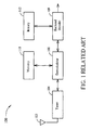
- FIG. 1 is a block diagram illustrating a conventional digital television receiver 100.
- the digital television receiver 100 includes an antenna 102, a tuner 104, a demodulator 106, a backend decoder 108, and a plurality of memories 110 and 112.
- the antenna 102 receives the digital television signal which is a radio frequency signal.
- the tuner 104 performs down-conversion and channel selection upon the received digital television signal
- the demodulator 106 performs demodulation upon an output of the tuner 104 for extracting a bit stream transmitted by the digital television signal.
- the backend decoder 108 generates video/audio signals to the following output devices (e.g., a television screen and a speaker) by performing a decoding operation, such as an MPEG (Moving Picture Experts Group) decoding operation, an H.264 decoding operation or an AVS (Audio Video coding Standard) decoding operation, upon the bit stream generated from the demodulator 106. In this way, program contents of a channel selected by the user are played on the output devices.
- a decoding operation such as an MPEG (Moving Picture Experts Group) decoding operation, an H.264 decoding operation or an AVS (Audio Video coding Standard) decoding operation, upon the bit stream generated from the demodulator 106.
- a decoding operation such as an MPEG (Moving Picture Experts Group) decoding operation, an H.264 decoding operation or an AVS (Audio Video coding Standard) decoding operation
- program contents of a channel selected by the user are played on the output devices.
- an interleaving operation may be performed to arrange the original data in a non-contiguous way before a transmitting end transmits the wireless communication signal, thereby mitigating the effect caused by channel fading.
- the digital television signal broadcasting when the transmitting end is equipped with an interleaver, the digital television receiver 100 at the receiving end is therefore required to have a corresponding deinterleaver.
- a convolutional deinterleaving operation is employed to arrange the original data in a non-contiguous way.
- the convolutional deinterleaver complying with the digital television standard defined by P.R.C. requires a large data buffer amount due to the shift registers implemented in a plurality of interleaving branches.
- the deinterleaving circuit in the demodulator 106 needs a large storage space to accomplish the deinterleaving operation.
- the conventional design often uses chip's external memory (e.g., the memory 110) to provide the desired storage space.
- the memory 110 is only accessible to the demodulator 106 (for example, the memory 110 is only accessible to the deinterleaving circuit within the demodulator 106) and the memory 112 is only accessible to the backend decoder 108, such a conventional hardware configuration lacks flexibility in the use of memories. Besides, the production cost cannot be effectively reduced due to these dedicated memories 110 and 112.
- FIG. 2 is a block diagram illustrating a generalized wireless communication receiver according to an exemplary embodiment of the present invention.
- the exemplary wireless communication receiver 200 includes, but is not limited to, a first signal processing circuit 202, a deinterleaver 204, a second signal processing circuit 206, and a data storage module 208.
- the same data storage module 208 is shared by the deinterleaver 204 and the second signal processing circuit 206 for data storage. That is, the data storage module 208 is not a dedicated storage element of either of the deinterleaver 204 and the second signal processing circuit 206.
- the first signal processing circuit 202 receives the wireless communication signal RF, and generates a first output data D1 to the deinterleaver 204 by performing a first signal processing operation according to the received wireless communication signal RF.
- the deinterleaver 204 stores the first output data D1 into the data storage module 208, and retrieves a deinterleaved data DD corresponding to the first output data D1 from the data storage module 208.
- the second signal processing circuit 206 receives the deinterleaved data DD generated from the deinterleaver 204, and generates a second output data D2 to the following circuit element(s) (not shown) by performing a second signal processing operation upon the received deinterleaved data DD.
- the wireless communication receiver 100 is a digital television receiver which receives a digital television signal transmitted in an orthogonal frequency division multiplexing (OFDM) manner (e.g., a wireless communication signal RF complying with the digital television standard defined by P.R.C.), and retrieves the digital television channel content (i.e., the second output data D2) from the received digital television signal and transmits the retrieved television channel content to the following output device (e.g., a screen and/or a speaker) for playback.
- OFDM orthogonal frequency division multiplexing
- the same data storage module 208 is shared by the deinterleaver 204 and the second signal processing circuit 206 (which is a backend circuit of the deinterleaver 204) for data storage.
- the data storage module 208 may be shared by the deinterleaver 204 and the first signal processing circuit 202 (which is a front-end circuit of the deinterleaver 204) for data storage. This also falls within the scope of the present invention.
- FIG. 2 only shows a generalized structure of the wireless communication receiver of the present invention for briefly illustrating that the data storage module used by the deinterleaver to accomplish the deinterleaving operation can be also used by other circuit(s) of the wireless communication receiver.
- the data storage module used by the deinterleaver to accomplish the deinterleaving operation can be also used by other circuit(s) of the wireless communication receiver.
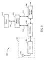
- FIG. 3 is a block diagram illustrating an exemplary embodiment of a wireless communication receiver of the present invention.
- the wireless communication receiver 300 includes an antenna 302, a tuner 304, a demodulator 306, a backend decoder 308, a memory controller 310, and a memory 312.
- the wireless communication receiver 300 shown in FIG. 3 is an exemplary implementation which employs the circuit structure shown in FIG. 2 .
- the antenna 302 receives a digital television signal, and then the tuner 304 performs down-conversion and channel selection upon the received digital television signal.
- the combination of the antenna 302 and the tuner 304 acts as a signal receiving circuit 305 for receiving the wireless communication signal (e.g., the digital television signal), and generates a received signal to the demodulator 306.
- the demodulator 306 demodulates an output of the tuner 304 to extract a bit stream transmitted via the digital television signal.
- the backend decoder 308 performs a decoding operation (e.g., an MPEG decoding operation, an H. 264 decoding operation or an AVS decoding operation) upon the bit stream generated from the demodulator 306, and accordingly generates a video/audio signal to the following output device (e.g., a screen and/or a speaker) for playback of the digital television channel content selected by the user.
- a decoding operation e.g., an MPEG decoding operation, an H. 264 decoding operation or an AVS decoding operation
- the data storage module 208 shown in FIG. 2 is realized by the memory 312, and the deinterleaver 204 shown in FIG. 2 is realized by a deinterleaver (not shown in FIG. 3 but will be detailed later) which is disposed in the demodulator 306.
- a combination of the antenna 302, the tuner 304, and a portion of the demodulator 306 (please note that this portion of the demodulator 306 does not have the aforementioned deinterleaver included therein) correspond to the first signal processing circuit 202 shown in FIG.
- the memory 312 such as a dynamic random access memory (DRAM) or a synchronous dynamic random access memory (SDRAM), is shared by the deinterleaver within the demodulator 306 and the backend decoder 308.
- DRAM dynamic random access memory
- SDRAM synchronous dynamic random access memory
- the memory controller 310 is responsible for arbitrating an access right of the memory 312 requested by the deinterleaver within the demodulator 306 and the backend decoder 308.
- the memory controller 310 performs write operations/read operations upon the memory 312 according to the memory write requests/memory read requests.
- memory address and data are transmitted via a memory bus 316 coupled between the memory controller 310 and the memory 312.
- the deinterleaver within the demodulator 306 and the backend decoder 308 share the memory 312 through the same memory bus 316.
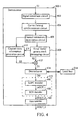
- FIG. 4 is a diagram illustrating a first exemplary embodiment of the demodulator 306 shown in FIG. 3 .
- the demodulator 306-1 includes, but is not limited to, a signal conversion circuit 402, a carrier/timing synchronization circuit 404, a channel estimation/equalization circuit 406, an error vector generation & demapping circuit 408, a channel state information generation circuit 410, a multiplier 412, a deinterleaver 414, an error-correction decoding module 41 5, and a descrambler 420.
- the received signal S1 may be an intermediate frequency (IF) signal or a baseband signal. If the received signal S1 is an IF signal, the demodulator 306 requires an additional down-conversion circuit (not shown) implemented therein for converting the IF signal into a baseband signal, and feeds the baseband signal into the signal conversion circuit 402 for analog-to-digital conversion. On the other hand, if the received signal S1 generated from the tuner 304 is already a baseband signal, the received signal S1 is directly fed into the signal conversion circuit 402 for analog-to-digital conversion.
- IF intermediate frequency
- the demodulator 306 requires an additional down-conversion circuit (not shown) implemented therein for converting the IF signal into a baseband signal, and feeds the baseband signal into the signal conversion circuit 402 for analog-to-digital conversion.
- the received signal S1 generated from the tuner 304 is already a baseband signal, the received signal S1 is directly fed into the signal conversion circuit 402 for analog-to-digital conversion.
- the carrier/timing synchronization circuit 404 makes the receiving end synchronized with the transmitting end to thereby allow the receiving end to correctly deal with OFDM symbols transmitted by the wireless communication signal.
- the channel estimation/equalization circuit 406 is utilized to perform channel estimation/equalization. Based on an output of the channel estimation/equalization circuit 406, the error vector generation & demapping circuit 408 generates an error vector EV to the channel state information generation circuit 410 and a demapping output S2 to the multiplier 41 2, wherein the demapping output S2 is a soft decision output and therefore contains a plurality of soft decision bits.
- the channel state information generation circuit 410 estimates the quality of the received symbols/bits by referring to the output of the channel estimation/equalization circuit 406 and/or the error vector EV, and accordingly generates the channel state information S3.
- the multiplier 41 2 generates the first output data D1 to the deinterleaver 414 according to the demapping output S2 and the channel state information S3.
- the first output data D1 is a soft decision output rather than a hard decision output.
- the deinterleaver 414 uses the memory 312 shown in FIG. 3 as the storage required to accomplish the deinterleaving operation. Therefore, the deinterleaver 414 accesses the memory 312 via the local bus 314.
- the deinterleaver 414 stores the first output data D1 into the memory 312 and then retrieves a deinterleaved data DD corresponding to the first output data D1 from the memory 312 via the local bus 314 and the memory controller 310 shown in FIG. 3 .
- An error-correction decoding operation is required to process the deinterleaved data DD.
- the error-correction decoding module 415 employed for performing the error-correction decoding operation therefore contains an LDPC decoder 416 and a BCH decoder 418, wherein the LDPC decoder 416 generates an LDPC decoding output DOUT_1 by performing an LDPC decoding operation upon the deinterleaved data DD, and the BCH decoder 418 generates a BCH decoding output DOUT_2 by performing a BCH decoding operation upon the LDPC decoding output DOUT_1.
- LDPC low-density parity-check
- BCH Bose-Chaudhuri-Hocquengham
- the transmitting end may use a scrambler to perform a scrambling operation upon data to be transmitted to thereby avoid a long sequence of consecutive 0's or 1's. Therefore, regarding the receiving end, the demodulator 316-1 in this exemplary embodiment has the corresponding descrambler 420 implemented therein to perform a descrambling operation upon the BCH decoding output DOUT_2 generated from the BCH decoder 418. The descrambler 420 therefore outputs a bit stream DOUT_3 to a following processing circuit, such as the backend decoder 308 shown in FIG. 3 .
- the deinterleaver 414 is used to deinterleave a product of the demapping output S2 and the channel state information S3.
- this is for illustrative purposes only, and is not mean to be a limitation of the present invention.
- FIG. 5 is a diagram illustrating a second exemplary embodiment of the demodulator 306 shown in FIG. 3 .
- the demodulator 306-2 includes, but is not limited to, a signal conversion circuit 502, a carrier/timing synchronization circuit 504, a channel estimation/equalization circuit 506, an error vector generation circuit 508, a channel state information generation circuit 510, a deinterleaver 512, a demapping circuit 514, a multiplier 516, an error-correction decoding module 517, and a descrambler 522, wherein the error-correction decoding module 517 includes an LDPC decoder 518 and a BCH decoder 520.
- the deinterleaver 512 respectively stores the channel estimation/equalization output S4 and the channel state information S3 into the memory 312 and respectively retrieves a deinterleaved data DD_1 corresponding to the channel estimation/equalization output S4 and a deinterleaved data DD_2 corresponding to the channel state information S3 from the memory 312 via the local bus 314 and the memory controller 310 shown in FIG. 3 .
- the first input data received by the deinterleaver 512 includes the channel estimation/equalization output S4 and the channel state information S3, and a deinterleaved data corresponding to the first input data includes the deinterleaved data DD_1 and the deinterleaved data DD_2.
- the deinterleaved data DD_1 is further processed by the demapping circuit 514, and the demapping circuit 514 accordingly generates a demapping output S2.
- the multiplier 516 generates an output according to the demapping output S2 and the deinterleaved data DD_2 corresponding to the channel state information S3, and then the output of the multiplier 516 is processed by error-correction decoding operations sequentially performed by the LDPC decoder 518 and the BCH decoder 520. After an output of the BCH decoder 520 is descrambled by the descrambler 522, a desired bit stream is generated from the demodulator 306-2 to a following processing circuit, such as the backend decoder 308 shown in FIG. 3 .
- a person skilled in the art can readily understand the operations and functions of elements shown in FIG. 5 after reading above paragraphs directed to the exemplary embodiment shown in FIG. 4 . Further description is therefore omitted here for brevity.
- the deinterleaver 414/512 of the demodulator 306-1 /306-2 shares the same memory 312 with the backend decoder 308.
- the present invention therefore further proposes a scheme for elastically adjusting a storage space allocation of the memory 312.
- the demapping output S2 is a soft decision output and contains a plurality of soft bits. As known to those skilled in the art, each soft decision bit is composed of a plurality of bits.
- the channel estimation/equalization output S4 also contains a plurality of soft decision bits each being composed of a plurality of bits.
- the deinterleaver 414/512 proposed in the present invention is used for processing a soft decision output rather than a hard decision output.
- the deinterleaver 414/512 can selectively reduce the number of bits in the soft decision bit that are actually stored into the memory 312. That is, the deinterleaver 414/512 can selectively reduce the bit width of the soft decision bit stored into the memory 312. In this way, the storage space requirement of the deinterleaving operation performed by the deinterleaver 414/512 can be lowered. In a condition where the memory 312 has a limited storage capacity, the available storage space in the memory 312 that is allocated to the backend decoder 308 can be effectively increased.
- FIG. 6A and FIG. 6B are diagrams illustrating different exemplary memory space configurations corresponding to the memory 312 shown in FIG. 3 .
- the backend decoder 308 only uses the storage space B, and the storage space A allocated to the deinterleaver 414/512 allows the deinterleaver 414/512 to store each complete soft decision bit into the memory 312.
- the second memory space configuration as shown in FIG. 6B is employed under the same total storage capacity of the memory 312.
- the storage space A' is smaller than the storage space A
- the storage space B' is larger than the storage space B.
- the deinterleaver 414/512 may reduce the number of bits in each soft decision bit when storing the soft decision bit into the memory 312.
- the write operation performed by the deinterleaver 414/512 drops one bit of each soft decision bit. That is, each soft decision bit has one missing bit after the deinterleaving operation is performed.
- the missing bit is padded with "0" to thereby allow the LDPC decoder to accomplish the LDPC decoding operation.
- the present invention proposes dynamically adjusting the bit width of data stored into the memory 312 for optimizing the use of the limited storage capacity of the memory 312 with slight receiver performance degradation or no receiver performance degradation.
- FIG. 7 is a third exemplary embodiment of the demodulator 306 shown in FIG. 3 .
- the exemplary embodiment shown in FIG. 7 is similar to that shown in FIG. 4 , and the major difference therebetween is that the demodulator 306-3 has an additional local buffer 702 disposed between the deinterleaver 414 and the local bus 314.
- the local buffer 702 and the deinterleaver 414 are both disposed inside the same chip (i.e., the same demodulator chip); however, the memory 312 shown in FIG. 3 is disposed outside of the chip.
- the bit width of the first output data D1 (which is a soft decision output) is M.
- the write operation performed by the deinterleaver 414 drops N bits in each soft decision bit of the first output data D1, wherein each soft decision bit of the first output data D1 contains M bits in total. That is, when each soft decision bit of the first output data D1 is to be buffered in the local buffer 702, only (M-N) bits will be actually stored into the local buffer 702.
- the local buffer 702 outputs each buffered soft decision bit having (M-N) bits to the external memory 312 via the local bus 314.
- the local buffer 702 may further have the transmission format conversion function. That is, supposing that the bit width of each soft decision bit in the first output data D1 is different from the bus width of the memory 312, the local buffer 702 buffers each soft decision bit in the first output data D1, and then transmits the buffered data to the memory 312 according to the bus width of the memory 312.
- each data set of the first output data D1 e.g., each soft decision bit of the first output data D1
- each data transmission between the local buffer 702 and the memory 312 follows a second bit width different from the first bit width.
- the memory 312 transmits the deinterleaved data to the local buffer 702 according to its bus width, and then the deinterleaver 414 reads each deinterleaved soft decision bit from the local buffer 702.
- the local buffer 702 may further improve the overall system performance due to reduced number of times of reading data from and/or writing data into the memory 312.
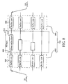
- FIG. 8 is an exemplary embodiment of the local buffer shown in FIG. 7 .
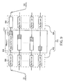
- the local buffer 702 includes an input buffer 802 and an output buffer 804, wherein the input buffer 802 and the output buffer 804 have a plurality of buffer units 806, respectively.
- each of the buffer units 806 has the same storage capacity. For example, each buffer unit 806 has the same storage capacity for buffering 16 OFDM symbols.
- a plurality of deinterleaving branches 808 are required for accomplishing the convolutional deinterleaving operation.
- data buffer blocks 808 with different buffer lengths are disposed at (Y-1) deinterleaving branches, respectively, wherein the operation of each data buffer block 808 is similar to that of a shift register.
- a buffer unit 806 is disposed at each deinterleaving branch 808.
- a buffer unit 806 is disposed at each deinterleaving branch.
- the buffer unit 806 When a data amount of the first output data D1 buffered in a buffer unit 806 reaches a predetermined value (e.g., the buffer unit 806 is full), the buffer unit 806 continuously writes its buffered data into the memory 312 through the corresponding deinterleaving branch. In other words, only when the accumulated data of the input buffer 802 that is to be stored into the memory 312 reaches a certain data amount, the input buffer 802 performs one write operation. Regarding the output buffer 804, the memory 312 continuously outputs data to a corresponding buffer unit 806 in the output buffer 804 until a data amount of buffered data in the output buffer 804 reaches a predetermined value (e.g., the output buffer 804 is full).
- a predetermined value e.g., the buffer unit 806 is full
- the deinterleaver 414 reads the desired deinterleaved data DD from the output buffer 804. That is, in one read operation, the memory 312 continuously outputs data to the output buffer 804 until the accumulated data of the output buffer 804 that is to be transmitted to the deinterleaver 414 reaches a certain data amount.
- the deinterleaving operation requires frequent write operations and read operations performed upon the memory 312.
- the memory 312 may be used by the backend decoder 308 for data storage.
- the frequent memory accesses of the memory 312 may degrade the overall system performance.
- the number of times of writing data into and/or reading data from the memory 312 can be greatly reduced, thereby mitigating the influence on the backend decoder 308 that is resulted from the memory accesses performed by the deinterleaver 414. In this way, the overall system performance can be greatly improved.
- the LDPC decoder uses blocks as basic units to deal with the decoding of LDPC codes. For example, one block may contain 7488 bits. Therefore, regarding each deinterleaving branch, the present invention further allocates additional buffer space in the shared memory for the LDPC decoder of the demodulator, wherein the shared memory is used by the backend decoder (e.g., an MPEG decoder, an H.264 decoder, or an AVS decoder) and the deinterleaver in the demodulator. In this way, when performing the read operation, the deinterleaver is capable of feeding a great amount of deinterleaved data, even a data amount of a whole block, into the LDPC decoder. As shown in FIG.
- the backend decoder e.g., an MPEG decoder, an H.264 decoder, or an AVS decoder
- the memory 312 includes a plurality of data buffer blocks 910 respectively corresponding to the deinterleaving branches 808. Compared to the memory 312 shown in FIG. 8 , the memory 312 in FIG. 9 has one additional buffer space allocated to each deinterleaving branch 808. Please note that each additionally allocated buffer space is represented by an area marked by oblique lines in FIG. 9 . It should be noted that the size of each additionally allocated buffer space shown in FIG. 9 is for illustrative purposes only. That is, the size of each additionally allocated buffer space may be adjusted, depending upon the actual design requirement/consideration.
- the buffer lengths of the data buffer blocks 910 are greater than minimum buffer lengths required by the corresponding deinterleaving branches 808 involved in performing the convolutional deinterleaving operation (e.g., the buffer lengths of the data buffer blocks 810 shown in FIG. 8 ), respectively.
- the conventional deinterleaver When accessing the memory, the conventional deinterleaver has to write one symbol into the memory immediately after one symbol is read from the memory.
- the exemplary deinterleaver of the present invention when accessing the memory 312, the exemplary deinterleaver of the present invention is not required to write N symbols into the memory 312 immediately after N symbols are read from the memory 312 due to the fact that each deinterleaving branch 808 has additionally allocated buffer space. Therefore, the use of the exemplary deinterleaver of the present invention is more flexible.
- the deinterleaver 414 cooperates with the memory 312 which has additional buffer space allocated therein and the above-mentioned local buffer 702 to thereby gain the above-mentioned benefits/advantages.
- this is for illustrative purposes only, and is not meant to be a limitation of the present invention. That is, in another exemplary embodiment, the deinterleaver 414 may only cooperate with the memory 312 having additional buffer space allocated therein. This also falls within the scope of the present invention.
- the local buffer may be employed in the exemplary embodiment shown in FIG. 5 .
- FIG. 10 is a fourth exemplary embodiment of the demodulator shown in FIG. 3 .
- the exemplary embodiment shown in FIG. 10 is similar to that shown in FIG. 5 , and the major difference therebetween is that the demodulator 306-4 has an additional local buffer 1002 implemented therein.
- the local buffer 1002 and the deinterleaver 512 are both disposed inside the same chip (e.g., the demodulator chip), whereas the memory 312 shown in FIG. 3 is disposed outside of the chip.
- the operation and function of the local buffer 1002 are similar to that of local buffers implemented in the exemplary embodiments shown in FIG. 8 and FIG. 9 , further description is therefore omitted here for brevity.
- the wireless communication receiving method includes the following steps: performing a first signal processing operation for receiving a wireless communication signal and generating a first output data according to the wireless communication signal; performing a deinterleaving operation for storing the first output data into a data storage module and retrieving a deinterleaved data corresponding to the first output data from the data storage module; and performing a second signal processing operation for generating a second output data according to the deinterleaved data.
- the data storage module is shared by the deinterleaving operation and at least one of the first signal processing operation and the second signal processing operation for data storage.
- the exemplary wireless communication receiving method of the present invention may be employed in a digital television receiver, such as a receiver complying with the digital television standard defined by P.R.C.
- a digital television receiver such as a receiver complying with the digital television standard defined by P.R.C.
- any digital television receiver using the exemplary wireless communication receiving method for allowing the deinterleaver and other signal processing circuit(s) to share the same data storage module for data storage falls within the scope fo the present invention.
Landscapes
- Engineering & Computer Science (AREA)
- Signal Processing (AREA)
- Multimedia (AREA)
- Computer Networks & Wireless Communication (AREA)
- Error Detection And Correction (AREA)
- Detection And Prevention Of Errors In Transmission (AREA)
- Circuits Of Receivers In General (AREA)
Claims (15)
- Récepteur de communication sans fil (200, 300), comportant :un module de stockage de données (208, 312) ;un désentrelaceur (204, 414, 512), couplé au module de stockage de données (208, 312), en vue de stocker des premières données de sortie dans le module de stockage de données (208, 312), et d'extraire des données désentrelacées correspondant aux premières données de sortie, à partir du module de stockage de données (208, 312) ; etune pluralité de circuits de traitement de signaux, comportant :un premier circuit de traitement de signaux (202), couplé au désentrelaceur (204, 414, 512), en vue de recevoir un signal de communication sans fil, et de générer les premières données de sortie en mettant en oeuvre une première opération de traitement de signaux selon le signal de communication sans fil ; etun second circuit de traitement de signaux (206), couplé au désentrelaceur (204, 414, 512), pour générer des secondes données de sortie en mettant en oeuvre une seconde opération de traitement de signaux selon les données désentrelacées ;dans lequel le module de stockage de données (208, 312) est partagé par le désentrelaceur (204, 414, 512) et au moins l'un des circuits de traitement de signaux pour le stockage de données ; le désentrelaceur (204, 414, 512) est utilisé pour mettre en oeuvre une opération de désentrelacement convolutionnel ; le module de stockage de données (208, 312) présente des espaces de mise en mémoire tampon qui lui sont affectés en vue d'agir en tant qu'une pluralité de blocs de mise en mémoire tampon de données (910) correspondant à une pluralité de branches de désentrelacement (808), respectivement ; chacun des blocs de mise en mémoire tampon de données affectés (910) reçoit une partie des premières données de sortie stockées dans le module de stockage de données (208, 312) et génère en sortie une partie des données désentrelacées générées à partir du module de stockage de données (208, 312), et les longueurs de mémoire tampon des blocs de mise en mémoire tampon de données (910) sont supérieures aux longueurs de mémoire tampon minimales requises par les branches de désentrelacement correspondantes (808) impliquées dans la mise en oeuvre de l'opération de désentrelacement convolutionnel, respectivement, dans lequel le stockage du module de stockage (208, 312) est affecté de manière souple au désentrelaceur (204, 414, 512) ;dans lequel le stockage du désentrelaceur traite une sortie de décision logicielle, dans lequel, en fonction de la mémoire à disposition du désentrelaceur, la largeur de bits de données stockées dans le module de stockage de données par le désentrelaceur est ajustée dynamiquement en réduisant de manière sélective le nombre de bits dans le bit de décision logicielle qui sont réellement stockés dans le module de stockage de données (312) ; dans lequel chaque bit de décision logicielle est constitué d'une pluralité de bits.
- Récepteur de communication sans fil (200, 300) selon la revendication 1, caractérisé en ce que le module de stockage de données (208, 312) est partagé par le désentrelaceur (204, 414, 512) et le second circuit de traitement de signaux (206), et le premier circuit de traitement de signaux (202) comporte :un circuit de réception de signaux (305), pour recevoir le signal de communication sans fil et générer en conséquence un signal reçu ;un circuit de démappage (408), pour générer une sortie de démappage selon le signal reçu ;un circuit de génération d'informations d'état de canal (410), pour générer des informations d'état de canal ; etun multiplicateur (412), couplé au circuit de démappage (408), au circuit de génération d'informations d'état de canal (410), et au désentrelaceur (204, 414), pour générer les premières données de sortie vers le désentrelaceur (204, 414) selon la sortie de démappage et les informations d'état de canal.
- Récepteur de communication sans fil (200, 300) selon la revendication 1, caractérisé en ce que le module de stockage de données (208, 312) est partagé par le désentrelaceur (204, 512) et le second circuit de traitement de signaux (206), et le premier circuit de traitement de signaux (202) comporte :un circuit de réception de signaux (305) pour recevoir le signal de communication sans fil et générer en conséquence un signal reçu ;un circuit d'égalisation / estimation de canal (506) pour générer une sortie d'égalisation / estimation de canal en mettant en oeuvre une égalisation / estimation de canal selon le signal reçu ; etun circuit de génération d'informations d'état de canal (510) pour générer des informations d'état de canal ;où le premier signal de sortie inclut la sortie d'égalisation / estimation de canal et les informations d'état de canal ; et le désentrelaceur (204, 512) est couplé au circuit d'égalisation / estimation de canal (506) et au circuit de génération d'informations d'état de canal (510), et utilisé pour stocker la sortie d'égalisation / estimation de canal et les informations d'état de canal dans le module de stockage de données (208, 312), respectivement, et extraire des données désentrelacées correspondant à la sortie d'égalisation / estimation de canal et des données désentrelacées correspondant aux informations d'état de canal, à partir du module de stockage de données (208, 312), respectivement.
- Récepteur de communication sans fil (200, 300) selon la revendication 1, caractérisé en ce que le module de stockage de données (208, 312) est partagé par le désentrelaceur (204, 414, 512) et le second circuit de traitement de signaux (206) pour le stockage de données, le désentrelaceur (204, 414, 512) est agencé dans une puce, et le module de stockage de données (208, 312) et le second circuit de traitement de signaux (206) sont agencés en dehors de la puce.
- Procédé de réception de communication sans fil, comportant :la mise en oeuvre d'une première opération de traitement de signaux destinée à recevoir un signal de communication sans fil et à générer des premières données de sortie selon le signal de communication sans fil ;la mise en oeuvre d'une opération de désentrelacement destinée à stocker les premières données de sortie dans un module de stockage de données (208, 312) et à extraire des données désentrelacées correspondant aux premières données de sortie, à partir du module de stockage de données (208, 312) ; etla mise en oeuvre d'une seconde opération de traitement de signaux destinée à générer des secondes données de sortie selon les données désentrelacées ;dans lequel le module de stockage de données (208, 312) est partagé par l'opération de désentrelacement et au moins l'une de la première opération de traitement de signaux et de la seconde opération de traitement de signaux pour le stockage de données ; l'opération de désentrelacement est une opération de désentrelacement convolutionnel ; le module de stockage de données (208, 312) présente des espaces de mise en mémoire tampon qui lui sont affectés en vue d'agir en tant qu'une pluralité de blocs de mise en mémoire tampon de données (910) correspondant à une pluralité de branches de désentrelacement (808), respectivement ; chacun des blocs de mise en mémoire tampon de données affectés (910) reçoit une partie des premières données de sortie stockées dans le module de stockage de données (208, 312) et génère en sortie une partie des données désentrelacées générées à partir du module de stockage de données (208, 312), et les longueurs de mémoire tampon des blocs de mise en mémoire tampon de données (910) sont supérieures aux longueurs de mémoire tampon minimales requises par les branches de désentrelacement correspondantes (808) impliquées dans la mise en oeuvre de l'opération de désentrelacement convolutionnel, respectivement
dans lequel le stockage du module de stockage (208, 312) est affecté de manière souple à l'opération de désentrelacement ;
dans lequel le stockage du désentrelaceur traite une sortie de décision logicielle, dans lequel, en fonction de la mémoire à disposition du désentrelaceur, la largeur de bits de données stockées dans le module de stockage de données par le désentrelaceur est ajustée dynamiquement en réduisant de manière sélective le nombre de bits dans le bit de décision logicielle qui sont réellement stockés dans le module de stockage de données (312) ; dans lequel chaque bit de décision logicielle est constitué d'une pluralité de bits. - Procédé de réception de communication sans fil selon la revendication 5, caractérisé en ce que le module de stockage de données (208, 312) est partagé par l'opération de désentrelacement et la seconde opération de traitement de signaux, et la première opération de traitement de signaux comporte :la réception du signal de communication sans fil et la génération, en conséquence, d'un signal reçu ;la génération d'une sortie de démappage selon le signal reçu ;la génération d'informations d'état de canal ; etla génération des premières données de sortie selon un produit de la sortie de démappage et des informations d'état de canal.
- Procédé de réception de communication sans fil selon la revendication 5, caractérisé en ce que le module de stockage de données (208, 312) est partagé par l'opération de désentrelacement et la seconde opération de traitement de signaux ; la première opération de traitement de signaux comporte : la réception du signal de communication sans fil et la génération, en conséquence, d'un signal reçu, la génération d'informations d'état de canal, et la génération d'une sortie d'égalisation /estimation de canal en mettant en oeuvre une égalisation / estimation de canal selon le signal reçu ; le premier signal de sortie inclut la sortie d'égalisation / estimation de canal et les informations d'état de canal ; et l'opération de désentrelacement stocke la sortie d'égalisation / estimation de canal et les informations d'état de canal dans le module de stockage de données (208, 312), respectivement, et extrait des données désentrelacées correspondant à la sortie d'égalisation / estimation de canal et des données désentrelacées correspondant aux informations d'état de canal, à partir du module de stockage de données (208, 312), respectivement.
- Procédé de réception de communication sans fil selon la revendication 5, caractérisé par :la fourniture d'un module de mise en mémoire tampon de données (702), et l'utilisation du module de mise en mémoire tampon de données (702) en vue de mettre en mémoire tampon les premières données de sortie générées à partir de l'opération de désentrelacement dans le module de stockage de données (208, 312) et de mettre en mémoire tampon les données désentrelacées lues à partir du module de stockage de données (208, 312) ;dans lequel les premières données de sortie correspondent à une première largeur de bits, le module de mise en mémoire tampon de données (702) et le module de stockage de données (208, 312) transmettent mutuellement des données selon une seconde largeur de bits, et la première largeur de bits est différente de la seconde largeur de bits.
- Procédé de réception de communication sans fil selon la revendication 5, caractérisé en ce que le module de stockage de données (208, 312) est partagé par l'opération de désentrelacement et la seconde opération de traitement de signaux pour le stockage de données, l'opération de désentrelacement est mise en oeuvre dans une puce, le module de stockage de données (208, 312) est agencé en dehors de la puce, et la seconde opération de traitement de signaux est mise en oeuvre en dehors de la puce.
- Récepteur de communication sans fil (200, 300) selon la revendication 1, comportant :un bus de mémoire (316), couplé au module de stockage de données (208, 312) ;dans lequel le désentrelaceur (204, 414, 514) et au moins l'un des circuits de traitement de signaux accèdent au module de stockage de données (208, 312) par l'intermédiaire du bus de mémoire (316) ;
- Récepteur de communication sans fil (200, 300) selon la revendication 10, caractérisé par :un module de mise en mémoire tampon de données (702), couplé entre le module de stockage de données (208, 312) et le désentrelaceur (204, 414, 514), en vue de mettre en mémoire tampon les données transmises entre le module de stockage de données (208, 312) et le désentrelaceur (204, 414, 514) ;dans lequel les premières données de sortie correspondent à une première largeur de bits, le bus de mémoire présente une seconde largeur de bits, et la première largeur de bits est différente de la seconde largeur de bits.
- Récepteur de télévision (200, 300), comportant :un module de stockage de données (208, 312) ;un démodulateur (306, 306-1, 306-2, 306-3, 306-4), destiné à recevoir et démoduler un signal de télévision numérique et à générer en conséquence un flux de bits, le démodulateur (306, 306-1, 306-2, 306-3, 306-4) comportant :un premier circuit de traitement de signaux, pour générer des premières données de sortie en mettant en oeuvre une première opération de traitement de signaux selon le signal de télévision numérique ;un désentrelaceur (204, 414, 512), couplé au premier circuit de traitement de signaux (202) et au module de stockage de données (208, 312), en vue de stocker les premières données de sortie dans le module de stockage de données (208, 312) et d'extraire des données désentrelacées correspondant aux premières données de sortie, à partir du module de stockage de données (208, 312) ;un module de décodage de correction d'erreur (415, 517), couplé au désentrelaceur (204, 414, 512), pour mettre en oeuvre une opération de décodage de correction d'erreur selon les données désentrelacées ; etun désembrouilleur (420, 522), couplé au module de décodage de correction d'erreur (415, 517), pour générer le flux de bits en mettant en oeuvre une opération de désembrouillage selon une sortie du module de décodage de correction d'erreur (415, 517) ; etun décodeur dorsal (308), couplé au démodulateur (306, 306-1, 306-2, 306-3, 306-4), pour recevoir et décoder le flux de bits ;dans lequel le récepteur de télévision (200, 300) présente un second circuit de traitement de signaux pour générer des secondes données de sortie en mettant en oeuvre une seconde opération de traitement de signaux selon les données désentrelacées, le second circuit de traitement de signaux comporte le module de décodage de correction d'erreur (415, 517), le désembrouilleur (420, 522), et le décodeur dorsal (308), et une sortie du décodeur dorsal (308) constitue les secondes données de sortie ; le module de stockage de données (208, 312) est partagé par le désentrelaceur (204, 414, 512) et le décodeur dorsal (308) pour le stockage de données ; le désentrelaceur (204, 414, 512) est utilisé pour mettre en oeuvre une opération de désentrelacement convolutionnel ; le module de stockage de données (208, 312) présente des espaces de mise en mémoire tampon qui lui sont affectés en vue d'agir en tant qu'une pluralité de blocs de mise en mémoire tampon de données (910) correspondant à une pluralité de branches de désentrelacement (808), respectivement ; chacun des blocs de mise en mémoire tampon de données affectés (910) reçoit une partie des premières données de sortie stockées dans le module de stockage de données (208, 312) et génère en sortie une partie des données désentrelacées générées à partir du module de stockage de données (208, 312), et les longueurs de mémoire tampon des blocs de mise en mémoire tampon de données (910) sont supérieures aux longueurs de mémoire tampon minimales requises par les branches de désentrelacement correspondantes (808) impliquées dans la mise en oeuvre de l'opération de désentrelacement convolutionnel, respectivement ;dans lequel le stockage du module de stockage (208, 312) est affecté de manière souple au désentrelaceur (204, 414, 512) ;dans lequel le stockage du désentrelaceur traite une sortie de décision logicielle, dans lequel, en fonction de la mémoire à disposition du désentrelaceur, la largeur de bits de données stockées dans le module de stockage de données par le désentrelaceur est ajustée dynamiquement en réduisant de manière sélective le nombre de bits dans le bit de décision logicielle qui sont réellement stockés dans le module de stockage de données (312) ; dans lequel chaque bit de décision logicielle est constitué d'une pluralité de bits.
- Récepteur de télévision selon la revendication 12, caractérisé en ce que le premier circuit de traitement de signaux comporte :un circuit de démappage (408), pour générer une sortie de démappage selon un signal reçu dérivé du signal de télévision numérique ;un circuit de génération d'informations d'état de canal (410), pour générer des informations d'état de canal ; etun multiplicateur (412), couplé au circuit de démappage (408), au circuit de génération d'informations d'état de canal (410), et au désentrelaceur (204, 414), pour générer les premières données de sortie vers le désentrelaceur (204, 414) selon la sortie de démappage et les informations d'état de canal.
- Récepteur de télévision selon la revendication 12, caractérisé en ce que le premier circuit de traitement de signaux comporte : un circuit d'égalisation / estimation de canal (506) pour générer une sortie d'égalisation / estimation de canal en mettant en oeuvre une égalisation /estimation de canal selon un signal reçu dérivé du signal de télévision numérique, et un circuit de génération d'informations d'état de canal (510) pour générer des informations d'état de canal, où le premier signal de sortie inclut la sortie d'égalisation / estimation de canal et les informations d'état de canal ; et le désentrelaceur (512) est couplé au circuit d'égalisation / estimation de canal (506) et au circuit de génération d'informations d'état de canal (510), et utilisé pour stocker la sortie d'égalisation / estimation de canal et les informations d'état de canal dans le module de stockage de données (208, 312), respectivement, et pour extraire des données désentrelacées correspondant à la sortie d'égalisation / estimation de canal et des données désentrelacées correspondant aux informations d'état de canal à partir du module de stockage de données (208, 312), respectivement.
- Récepteur de communication sans fil (200, 300) selon la revendication 1, ou récepteur de télévision (200, 300) selon la revendication 12, caractérisé par :un module de mise en mémoire tampon de données (702), couplé entre le module de stockage de données (208, 312) et le désentrelaceur (204, 414, 512), en vue de mettre en mémoire tampon les données transmises entre le module de stockage de données (208, 312) et le désentrelaceur (204, 414, 512) ;dans lequel le module de mise en mémoire tampon de données (702) et le désentrelaceur (204, 414, 512) sont tous deux agencés à l'intérieur d'une puce, et le module de stockage de données (208, 312) est agencé en dehors de la puce.
Applications Claiming Priority (1)
| Application Number | Priority Date | Filing Date | Title |
|---|---|---|---|
| PCT/CN2008/070229 WO2009100612A1 (fr) | 2008-01-31 | 2008-01-31 | Récepteur de communication sans fil, procédé de réception de communication sans fil et récepteur de télévision |
Publications (3)
| Publication Number | Publication Date |
|---|---|
| EP2242265A1 EP2242265A1 (fr) | 2010-10-20 |
| EP2242265A4 EP2242265A4 (fr) | 2011-08-03 |
| EP2242265B1 true EP2242265B1 (fr) | 2013-04-24 |
Family
ID=40956629
Family Applications (1)
| Application Number | Title | Priority Date | Filing Date |
|---|---|---|---|
| EP08706606.4A Not-in-force EP2242265B1 (fr) | 2008-01-31 | 2008-01-31 | Récepteur de communication sans fil, procédé de réception de communication sans fil et récepteur de télévision |
Country Status (3)
| Country | Link |
|---|---|
| US (1) | US8804049B2 (fr) |
| EP (1) | EP2242265B1 (fr) |
| WO (1) | WO2009100612A1 (fr) |
Families Citing this family (7)
| Publication number | Priority date | Publication date | Assignee | Title |
|---|---|---|---|---|
| JP5299130B2 (ja) * | 2009-07-03 | 2013-09-25 | 富士通セミコンダクター株式会社 | 受信データ処理回路及び受信データ処理切り替え方法 |
| US20120050619A1 (en) * | 2010-08-30 | 2012-03-01 | Sony Corporation | Reception apparatus, reception method, transmission apparatus, transmission method, program, and broadcasting system |
| TWI520502B (zh) * | 2012-11-23 | 2016-02-01 | 晨星半導體股份有限公司 | 迴旋解交錯裝置及迴旋解交錯方法 |
| CN103856433B (zh) * | 2012-12-04 | 2017-10-31 | 晨星软件研发(深圳)有限公司 | 回旋解交错装置及回旋解交错方法 |
| US10340953B2 (en) * | 2015-05-19 | 2019-07-02 | Samsung Electronics Co., Ltd. | Method and apparatus for encoding and decoding low density parity check codes |
| US10879936B2 (en) * | 2018-08-23 | 2020-12-29 | Keysight Technologies, Inc. | Methods, systems, and computer readable media for de-interleaving data in a communication system |
| WO2023287415A1 (fr) * | 2021-07-14 | 2023-01-19 | Zeku, Inc. | Appareil et procédé d'estimation de canal à faible puissance |
Family Cites Families (14)
| Publication number | Priority date | Publication date | Assignee | Title |
|---|---|---|---|---|
| GB2325129B (en) | 1997-05-02 | 2002-06-19 | Lsi Logic Corp | Demodulating digital video broadcast signals |
| US7051171B1 (en) * | 2003-04-11 | 2006-05-23 | Broadlogic Network Technologies, Inc. | Method and system for providing a multi-channel interleaver/deinterleaver using SDRAM |
| US7610061B2 (en) | 2003-09-20 | 2009-10-27 | Samsung Electronics Co., Ltd. | Communication device and method having a common platform |
| US7600163B2 (en) * | 2003-09-23 | 2009-10-06 | Realtek Semiconductor Corp. | Convolutional interleaver and deinterleaver |
| WO2006044227A1 (fr) * | 2004-10-12 | 2006-04-27 | Aware, Inc. | Partage de ressources dans un environnement de telecommunications |
| US7284183B2 (en) | 2004-11-04 | 2007-10-16 | Mediatek Inc. | Method and apparatus for decoding multiword information |
| US7502408B2 (en) | 2005-04-21 | 2009-03-10 | Broadcom Corporation | RF transceiver having adaptive modulation |
| KR100796864B1 (ko) * | 2005-05-03 | 2008-01-22 | 엘지전자 주식회사 | 지상파 dmb 수신기에 있어서 채널 전환 제어방법 |
| US7779338B2 (en) | 2005-07-21 | 2010-08-17 | Realtek Semiconductor Corp. | Deinterleaver and dual-viterbi decoder architecture |
| CN101001337A (zh) | 2006-01-12 | 2007-07-18 | 深圳创维-Rgb电子有限公司 | 一种数字电视录像机及其录像实现方法 |
| US8284322B2 (en) | 2006-04-18 | 2012-10-09 | Marvell World Trade Ltd. | Shared memory multi video channel display apparatus and methods |
| US8755675B2 (en) | 2006-04-20 | 2014-06-17 | Texas Instruments Incorporated | Flexible and efficient memory utilization for high bandwidth receivers, integrated circuits, systems, methods and processes of manufacture |
| JP4773882B2 (ja) | 2006-05-24 | 2011-09-14 | 富士通セミコンダクター株式会社 | Ofdm受信装置及びofdm受信方法 |
| US20090015721A1 (en) * | 2007-07-09 | 2009-01-15 | Legend Silicon Corp. | Methods and apparatus using shared storage for cannel error correction and multimedia decoding and processing in a digital tv system |
-
2008
- 2008-01-31 EP EP08706606.4A patent/EP2242265B1/fr not_active Not-in-force
- 2008-01-31 US US12/865,398 patent/US8804049B2/en not_active Expired - Fee Related
- 2008-01-31 WO PCT/CN2008/070229 patent/WO2009100612A1/fr not_active Ceased
Also Published As
| Publication number | Publication date |
|---|---|
| EP2242265A4 (fr) | 2011-08-03 |
| US20100321586A1 (en) | 2010-12-23 |
| US8804049B2 (en) | 2014-08-12 |
| EP2242265A1 (fr) | 2010-10-20 |
| WO2009100612A1 (fr) | 2009-08-20 |
Similar Documents
| Publication | Publication Date | Title |
|---|---|---|
| EP2242265B1 (fr) | Récepteur de communication sans fil, procédé de réception de communication sans fil et récepteur de télévision | |
| CN101467354B (zh) | 交织器设备以及用于由交织器设备产生的信号的接收机 | |
| EP1856807B1 (fr) | Decodeurs turbo paralleles avec sortie multiplexee | |
| US20100283912A1 (en) | Apparatus for Demodulating Digital Video and Associated Method | |
| US9130593B2 (en) | Data processing method | |
| US20080028188A1 (en) | Time de-interleaver implementation using sdram in a tds-ofdm receiver | |
| EP1545126A2 (fr) | Circuit et récepteur de dispersion d'énergie | |
| US5563915A (en) | Data deinterleaver in a digital television signal decoding system | |
| TWI488448B (zh) | 用於疊代解碼器之擴充解交錯器 | |
| CN101860372B (zh) | 无线通信接收机和信号处理方法 | |
| CN101500099B (zh) | 无线通讯接收机、无线通讯接收方法与电视接收机 | |
| JP2011029833A (ja) | 復調装置、復調装置の制御方法、復調装置の制御プログラム、および復調装置の制御プログラムを記録した記録媒体 | |
| TWI524768B (zh) | 頻率解交錯與時間解交錯電路與方法以及數位電視之接收電路 | |
| US20090015721A1 (en) | Methods and apparatus using shared storage for cannel error correction and multimedia decoding and processing in a digital tv system | |
| TWI408959B (zh) | 解交錯器與其他電路共用資料儲存模組的無線通訊接收機、電視接收機與其相關方法 | |
| KR100565673B1 (ko) | 디지털 멀티미디어 방송 수신기에서 시간 역인터리버메모리 감소 방법 | |
| CN105721929B (zh) | 频率解交错与时间解交错电路与方法以及数字电视的接收电路 | |
| EP1553711A2 (fr) | Dispositif et procédé de desentrelacement pour récepteurs de diffusion numériques comprenant une mémoire de desentrelacement réduite | |
| KR100733767B1 (ko) | 시간 디인터리빙 장치 및 방법 | |
| CN101674092B (zh) | 一种支持数据帧长无缝变化的解交织器及其方法 | |
| Kang et al. | Area-efficient convolutional deinterleaver for mobile TV receiver | |
| CN100531164C (zh) | Dmb信号接收器的时间反交错存储器减少方法 | |
| KR101087104B1 (ko) | 디지털 멀티미디어 방송 수신장치에서의 채널 복호 방법 및장치 | |
| KR100628107B1 (ko) | 디지털 수신기의 주파수 역인터리빙 장치 및 방법 | |
| JP2006005490A (ja) | 復号処理装置、および当該復号処理装置を備えたデジタル信号受信装置 |
Legal Events
| Date | Code | Title | Description |
|---|---|---|---|
| PUAI | Public reference made under article 153(3) epc to a published international application that has entered the european phase |
Free format text: ORIGINAL CODE: 0009012 |
|
| 17P | Request for examination filed |
Effective date: 20100730 |
|
| AK | Designated contracting states |
Kind code of ref document: A1 Designated state(s): AT BE BG CH CY CZ DE DK EE ES FI FR GB GR HR HU IE IS IT LI LT LU LV MC MT NL NO PL PT RO SE SI SK TR |
|
| AX | Request for extension of the european patent |
Extension state: AL BA MK RS |
|
| DAX | Request for extension of the european patent (deleted) | ||
| RIC1 | Information provided on ipc code assigned before grant |
Ipc: H04L 1/00 20060101ALI20110617BHEP Ipc: H04L 27/26 20060101ALI20110617BHEP Ipc: H04N 7/06 20060101AFI20090907BHEP |
|
| A4 | Supplementary search report drawn up and despatched |
Effective date: 20110701 |
|
| 17Q | First examination report despatched |
Effective date: 20111222 |
|
| REG | Reference to a national code |
Ref country code: DE Ref legal event code: R079 Ref document number: 602008024054 Country of ref document: DE Free format text: PREVIOUS MAIN CLASS: H04N0007060000 Ipc: H04N0005440000 |
|
| GRAP | Despatch of communication of intention to grant a patent |
Free format text: ORIGINAL CODE: EPIDOSNIGR1 |
|
| RIC1 | Information provided on ipc code assigned before grant |
Ipc: H04N 21/4363 20110101ALI20121206BHEP Ipc: H04L 27/26 20060101ALI20121206BHEP Ipc: H04N 5/44 20110101AFI20121206BHEP Ipc: H04L 1/00 20060101ALI20121206BHEP |
|
| GRAS | Grant fee paid |
Free format text: ORIGINAL CODE: EPIDOSNIGR3 |
|
| GRAA | (expected) grant |
Free format text: ORIGINAL CODE: 0009210 |
|
| AK | Designated contracting states |
Kind code of ref document: B1 Designated state(s): AT BE BG CH CY CZ DE DK EE ES FI FR GB GR HR HU IE IS IT LI LT LU LV MC MT NL NO PL PT RO SE SI SK TR |
|
| REG | Reference to a national code |
Ref country code: GB Ref legal event code: FG4D |
|
| REG | Reference to a national code |
Ref country code: CH Ref legal event code: EP |
|
| REG | Reference to a national code |
Ref country code: AT Ref legal event code: REF Ref document number: 609212 Country of ref document: AT Kind code of ref document: T Effective date: 20130515 |
|
| REG | Reference to a national code |
Ref country code: IE Ref legal event code: FG4D |
|
| REG | Reference to a national code |
Ref country code: DE Ref legal event code: R096 Ref document number: 602008024054 Country of ref document: DE Effective date: 20130620 |
|
| REG | Reference to a national code |
Ref country code: AT Ref legal event code: MK05 Ref document number: 609212 Country of ref document: AT Kind code of ref document: T Effective date: 20130424 |
|
| REG | Reference to a national code |
Ref country code: LT Ref legal event code: MG4D |
|
| REG | Reference to a national code |
Ref country code: NL Ref legal event code: VDEP Effective date: 20130424 |
|
| PG25 | Lapsed in a contracting state [announced via postgrant information from national office to epo] |
Ref country code: AT Free format text: LAPSE BECAUSE OF FAILURE TO SUBMIT A TRANSLATION OF THE DESCRIPTION OR TO PAY THE FEE WITHIN THE PRESCRIBED TIME-LIMIT Effective date: 20130424 Ref country code: PT Free format text: LAPSE BECAUSE OF FAILURE TO SUBMIT A TRANSLATION OF THE DESCRIPTION OR TO PAY THE FEE WITHIN THE PRESCRIBED TIME-LIMIT Effective date: 20130826 Ref country code: NO Free format text: LAPSE BECAUSE OF FAILURE TO SUBMIT A TRANSLATION OF THE DESCRIPTION OR TO PAY THE FEE WITHIN THE PRESCRIBED TIME-LIMIT Effective date: 20130724 Ref country code: LT Free format text: LAPSE BECAUSE OF FAILURE TO SUBMIT A TRANSLATION OF THE DESCRIPTION OR TO PAY THE FEE WITHIN THE PRESCRIBED TIME-LIMIT Effective date: 20130424 Ref country code: ES Free format text: LAPSE BECAUSE OF FAILURE TO SUBMIT A TRANSLATION OF THE DESCRIPTION OR TO PAY THE FEE WITHIN THE PRESCRIBED TIME-LIMIT Effective date: 20130804 Ref country code: IS Free format text: LAPSE BECAUSE OF FAILURE TO SUBMIT A TRANSLATION OF THE DESCRIPTION OR TO PAY THE FEE WITHIN THE PRESCRIBED TIME-LIMIT Effective date: 20130824 Ref country code: FI Free format text: LAPSE BECAUSE OF FAILURE TO SUBMIT A TRANSLATION OF THE DESCRIPTION OR TO PAY THE FEE WITHIN THE PRESCRIBED TIME-LIMIT Effective date: 20130424 Ref country code: BE Free format text: LAPSE BECAUSE OF FAILURE TO SUBMIT A TRANSLATION OF THE DESCRIPTION OR TO PAY THE FEE WITHIN THE PRESCRIBED TIME-LIMIT Effective date: 20130424 Ref country code: GR Free format text: LAPSE BECAUSE OF FAILURE TO SUBMIT A TRANSLATION OF THE DESCRIPTION OR TO PAY THE FEE WITHIN THE PRESCRIBED TIME-LIMIT Effective date: 20130725 Ref country code: SE Free format text: LAPSE BECAUSE OF FAILURE TO SUBMIT A TRANSLATION OF THE DESCRIPTION OR TO PAY THE FEE WITHIN THE PRESCRIBED TIME-LIMIT Effective date: 20130424 Ref country code: SI Free format text: LAPSE BECAUSE OF FAILURE TO SUBMIT A TRANSLATION OF THE DESCRIPTION OR TO PAY THE FEE WITHIN THE PRESCRIBED TIME-LIMIT Effective date: 20130424 |
|
| PG25 | Lapsed in a contracting state [announced via postgrant information from national office to epo] |
Ref country code: PL Free format text: LAPSE BECAUSE OF FAILURE TO SUBMIT A TRANSLATION OF THE DESCRIPTION OR TO PAY THE FEE WITHIN THE PRESCRIBED TIME-LIMIT Effective date: 20130424 Ref country code: BG Free format text: LAPSE BECAUSE OF FAILURE TO SUBMIT A TRANSLATION OF THE DESCRIPTION OR TO PAY THE FEE WITHIN THE PRESCRIBED TIME-LIMIT Effective date: 20130724 Ref country code: CY Free format text: LAPSE BECAUSE OF FAILURE TO SUBMIT A TRANSLATION OF THE DESCRIPTION OR TO PAY THE FEE WITHIN THE PRESCRIBED TIME-LIMIT Effective date: 20130424 Ref country code: HR Free format text: LAPSE BECAUSE OF FAILURE TO SUBMIT A TRANSLATION OF THE DESCRIPTION OR TO PAY THE FEE WITHIN THE PRESCRIBED TIME-LIMIT Effective date: 20130424 Ref country code: LV Free format text: LAPSE BECAUSE OF FAILURE TO SUBMIT A TRANSLATION OF THE DESCRIPTION OR TO PAY THE FEE WITHIN THE PRESCRIBED TIME-LIMIT Effective date: 20130424 |
|
| PG25 | Lapsed in a contracting state [announced via postgrant information from national office to epo] |
Ref country code: EE Free format text: LAPSE BECAUSE OF FAILURE TO SUBMIT A TRANSLATION OF THE DESCRIPTION OR TO PAY THE FEE WITHIN THE PRESCRIBED TIME-LIMIT Effective date: 20130424 Ref country code: CZ Free format text: LAPSE BECAUSE OF FAILURE TO SUBMIT A TRANSLATION OF THE DESCRIPTION OR TO PAY THE FEE WITHIN THE PRESCRIBED TIME-LIMIT Effective date: 20130424 Ref country code: DK Free format text: LAPSE BECAUSE OF FAILURE TO SUBMIT A TRANSLATION OF THE DESCRIPTION OR TO PAY THE FEE WITHIN THE PRESCRIBED TIME-LIMIT Effective date: 20130424 Ref country code: SK Free format text: LAPSE BECAUSE OF FAILURE TO SUBMIT A TRANSLATION OF THE DESCRIPTION OR TO PAY THE FEE WITHIN THE PRESCRIBED TIME-LIMIT Effective date: 20130424 |
|
| PG25 | Lapsed in a contracting state [announced via postgrant information from national office to epo] |
Ref country code: RO Free format text: LAPSE BECAUSE OF FAILURE TO SUBMIT A TRANSLATION OF THE DESCRIPTION OR TO PAY THE FEE WITHIN THE PRESCRIBED TIME-LIMIT Effective date: 20130424 Ref country code: IT Free format text: LAPSE BECAUSE OF FAILURE TO SUBMIT A TRANSLATION OF THE DESCRIPTION OR TO PAY THE FEE WITHIN THE PRESCRIBED TIME-LIMIT Effective date: 20130424 Ref country code: NL Free format text: LAPSE BECAUSE OF FAILURE TO SUBMIT A TRANSLATION OF THE DESCRIPTION OR TO PAY THE FEE WITHIN THE PRESCRIBED TIME-LIMIT Effective date: 20130424 |
|
| PLBE | No opposition filed within time limit |
Free format text: ORIGINAL CODE: 0009261 |
|
| STAA | Information on the status of an ep patent application or granted ep patent |
Free format text: STATUS: NO OPPOSITION FILED WITHIN TIME LIMIT |
|
| 26N | No opposition filed |
Effective date: 20140127 |
|
| REG | Reference to a national code |
Ref country code: DE Ref legal event code: R097 Ref document number: 602008024054 Country of ref document: DE Effective date: 20140127 |
|
| PG25 | Lapsed in a contracting state [announced via postgrant information from national office to epo] |
Ref country code: MC Free format text: LAPSE BECAUSE OF FAILURE TO SUBMIT A TRANSLATION OF THE DESCRIPTION OR TO PAY THE FEE WITHIN THE PRESCRIBED TIME-LIMIT Effective date: 20130424 Ref country code: LU Free format text: LAPSE BECAUSE OF FAILURE TO SUBMIT A TRANSLATION OF THE DESCRIPTION OR TO PAY THE FEE WITHIN THE PRESCRIBED TIME-LIMIT Effective date: 20140131 |
|
| REG | Reference to a national code |
Ref country code: CH Ref legal event code: PL |
|
| PG25 | Lapsed in a contracting state [announced via postgrant information from national office to epo] |
Ref country code: LI Free format text: LAPSE BECAUSE OF NON-PAYMENT OF DUE FEES Effective date: 20140131 Ref country code: CH Free format text: LAPSE BECAUSE OF NON-PAYMENT OF DUE FEES Effective date: 20140131 |
|
| REG | Reference to a national code |
Ref country code: IE Ref legal event code: MM4A |
|
| PG25 | Lapsed in a contracting state [announced via postgrant information from national office to epo] |
Ref country code: IE Free format text: LAPSE BECAUSE OF NON-PAYMENT OF DUE FEES Effective date: 20140131 |
|
| REG | Reference to a national code |
Ref country code: FR Ref legal event code: PLFP Year of fee payment: 9 |
|
| PG25 | Lapsed in a contracting state [announced via postgrant information from national office to epo] |
Ref country code: MT Free format text: LAPSE BECAUSE OF FAILURE TO SUBMIT A TRANSLATION OF THE DESCRIPTION OR TO PAY THE FEE WITHIN THE PRESCRIBED TIME-LIMIT Effective date: 20130424 |
|
| PG25 | Lapsed in a contracting state [announced via postgrant information from national office to epo] |
Ref country code: TR Free format text: LAPSE BECAUSE OF FAILURE TO SUBMIT A TRANSLATION OF THE DESCRIPTION OR TO PAY THE FEE WITHIN THE PRESCRIBED TIME-LIMIT Effective date: 20130424 Ref country code: HU Free format text: LAPSE BECAUSE OF FAILURE TO SUBMIT A TRANSLATION OF THE DESCRIPTION OR TO PAY THE FEE WITHIN THE PRESCRIBED TIME-LIMIT; INVALID AB INITIO Effective date: 20080131 |
|
| REG | Reference to a national code |
Ref country code: FR Ref legal event code: PLFP Year of fee payment: 10 |
|
| REG | Reference to a national code |
Ref country code: FR Ref legal event code: PLFP Year of fee payment: 11 |
|
| PGFP | Annual fee paid to national office [announced via postgrant information from national office to epo] |
Ref country code: GB Payment date: 20200127 Year of fee payment: 13 Ref country code: DE Payment date: 20200129 Year of fee payment: 13 |
|
| PGFP | Annual fee paid to national office [announced via postgrant information from national office to epo] |
Ref country code: FR Payment date: 20200127 Year of fee payment: 13 |
|
| REG | Reference to a national code |
Ref country code: DE Ref legal event code: R119 Ref document number: 602008024054 Country of ref document: DE |
|
| GBPC | Gb: european patent ceased through non-payment of renewal fee |
Effective date: 20210131 |
|
| PG25 | Lapsed in a contracting state [announced via postgrant information from national office to epo] |
Ref country code: FR Free format text: LAPSE BECAUSE OF NON-PAYMENT OF DUE FEES Effective date: 20210131 |
|
| PG25 | Lapsed in a contracting state [announced via postgrant information from national office to epo] |
Ref country code: DE Free format text: LAPSE BECAUSE OF NON-PAYMENT OF DUE FEES Effective date: 20210803 Ref country code: GB Free format text: LAPSE BECAUSE OF NON-PAYMENT OF DUE FEES Effective date: 20210131 |