EP2243206B1 - Batteriesystem mit niedriger leistung - Google Patents
Batteriesystem mit niedriger leistung Download PDFInfo
- Publication number
- EP2243206B1 EP2243206B1 EP08872241.8A EP08872241A EP2243206B1 EP 2243206 B1 EP2243206 B1 EP 2243206B1 EP 08872241 A EP08872241 A EP 08872241A EP 2243206 B1 EP2243206 B1 EP 2243206B1
- Authority
- EP
- European Patent Office
- Prior art keywords
- coupled
- cell
- discrete
- logic device
- type logic
- Prior art date
- Legal status (The legal status is an assumption and is not a legal conclusion. Google has not performed a legal analysis and makes no representation as to the accuracy of the status listed.)
- Active
Links
Images


Classifications
-
- H—ELECTRICITY
- H02—GENERATION; CONVERSION OR DISTRIBUTION OF ELECTRIC POWER
- H02J—ELECTRIC POWER NETWORKS; CIRCUIT ARRANGEMENTS OR SYSTEMS FOR SUPPLYING OR DISTRIBUTING ELECTRIC POWER; SYSTEMS FOR STORING ELECTRIC ENERGY
- H02J7/00—Circuit arrangements for charging or discharging batteries or for supplying loads from batteries
- H02J7/50—Circuit arrangements for charging or discharging batteries or for supplying loads from batteries acting upon multiple batteries simultaneously or sequentially
- H02J7/52—Circuit arrangements for charging or discharging batteries or for supplying loads from batteries acting upon multiple batteries simultaneously or sequentially for charge balancing, e.g. equalisation of charge between batteries
- H02J7/54—Passive balancing, e.g. using resistors or parallel MOSFETs
-
- H—ELECTRICITY
- H01—ELECTRIC ELEMENTS
- H01M—PROCESSES OR MEANS, e.g. BATTERIES, FOR THE DIRECT CONVERSION OF CHEMICAL ENERGY INTO ELECTRICAL ENERGY
- H01M10/00—Secondary cells; Manufacture thereof
- H01M10/42—Methods or arrangements for servicing or maintenance of secondary cells or secondary half-cells
- H01M10/425—Structural combination with electronic components, e.g. electronic circuits integrated to the outside of the casing
-
- H—ELECTRICITY
- H01—ELECTRIC ELEMENTS
- H01M—PROCESSES OR MEANS, e.g. BATTERIES, FOR THE DIRECT CONVERSION OF CHEMICAL ENERGY INTO ELECTRICAL ENERGY
- H01M10/00—Secondary cells; Manufacture thereof
- H01M10/42—Methods or arrangements for servicing or maintenance of secondary cells or secondary half-cells
- H01M10/44—Methods for charging or discharging
- H01M10/441—Methods for charging or discharging for several batteries or cells simultaneously or sequentially
-
- H—ELECTRICITY
- H01—ELECTRIC ELEMENTS
- H01M—PROCESSES OR MEANS, e.g. BATTERIES, FOR THE DIRECT CONVERSION OF CHEMICAL ENERGY INTO ELECTRICAL ENERGY
- H01M10/00—Secondary cells; Manufacture thereof
- H01M10/42—Methods or arrangements for servicing or maintenance of secondary cells or secondary half-cells
- H01M10/425—Structural combination with electronic components, e.g. electronic circuits integrated to the outside of the casing
- H01M2010/4271—Battery management systems including electronic circuits, e.g. control of current or voltage to keep battery in healthy state, cell balancing
-
- Y—GENERAL TAGGING OF NEW TECHNOLOGICAL DEVELOPMENTS; GENERAL TAGGING OF CROSS-SECTIONAL TECHNOLOGIES SPANNING OVER SEVERAL SECTIONS OF THE IPC; TECHNICAL SUBJECTS COVERED BY FORMER USPC CROSS-REFERENCE ART COLLECTIONS [XRACs] AND DIGESTS
- Y02—TECHNOLOGIES OR APPLICATIONS FOR MITIGATION OR ADAPTATION AGAINST CLIMATE CHANGE
- Y02E—REDUCTION OF GREENHOUSE GAS [GHG] EMISSIONS, RELATED TO ENERGY GENERATION, TRANSMISSION OR DISTRIBUTION
- Y02E60/00—Enabling technologies; Technologies with a potential or indirect contribution to GHG emissions mitigation
- Y02E60/10—Energy storage using batteries
Definitions
- the present invention relates to a device and method for balancing charge between a plurality of storage batteries, and more specifically, to a low-loss battery balancing system that may be implemented, for example, in a low-power battery balancing application.
- Electronic monitoring and control applications require continuously supplied power from one or more reliable sources. These sources may generate power (e.g., solar cells, fossil fuel engines, hydroelectric, etc.) or may provide stored power when generated power is not available. If power is supplied from a combination of sources, the flow of energy supplied from these sources must be managed seamlessly. Power spikes or losses often risk an unrecoverable loss of system control, resulting in damage to equipment or possibly life-threatening situations.
- sources may generate power (e.g., solar cells, fossil fuel engines, hydroelectric, etc.) or may provide stored power when generated power is not available. If power is supplied from a combination of sources, the flow of energy supplied from these sources must be managed seamlessly. Power spikes or losses often risk an unrecoverable loss of system control, resulting in damage to equipment or possibly life-threatening situations.
- Storage batteries are often used as back-up power when generated power is not available.
- the individual cells of some types of batteries for example Lithium Ion batteries, may become unbalanced over continuous use. While these batteries may continue to function, the cell unbalancing may cause performance problems and lessen the overall lifespan of the battery.
- battery balancing systems are often employed to equalize the energy stored in the battery cells so that performance may be maximized.
- disturbances may include parasitic resistance that adversely affects the accuracy of cell voltages monitored by a microprocessor coupled to the balancing system, which may in turn impact overall system performance. More specifically, inaccurate measured voltages may result in incorrect control execution, false alarms and possibly even damage to the system.
- transformers may create losses due to core loss and IR loss resulting from magnetizing current. These losses may be acceptable for larger battery cells, but may create a substantial negative impact in system performance with respect to smaller cells.
- US 2004/246635 A1 discloses a battery balancing circuit which transfers energy between a plurality of battery cells by charging and discharging of shared capacitors.
- the present invention is defined in claim 1 and includes a system for balancing the charge level of a plurality of electrically coupled battery units.
- the system configuration may utilize an architecture and/or methodology that is more appropriate for lower power applications.
- the present invention in accordance with at least one embodiment, may provide a battery balancing system that implements low loss charge balancing circuits in a compact configuration suitable for a multitude of applications, such as smaller cell battery balancing.
- a plurality of battery units are electrically coupled in order to form a power storage system.
- These battery units include both batteries and charge balancing circuitry.
- these components may all be incorporated within the battery unit housing.
- the batteries with each battery unit may be electronically coupled to each other, for example in a series configuration, and also to a system clock.
- the system clock is electronically coupled to the charge balancing circuitry in order to synchronize the activity of these circuits.
- the present invention in accordance with the clock signal, allows current to flow from higher charge batteries to lower charge batteries in order to equalize the charge amongst all of the batteries.
- This battery balancing may be accomplished with little loss due to, for example, circuit componentry, because the configuration of various embodiments of the present invention has been designed to reduce the loss for smaller batteries.
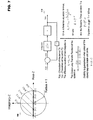
- Satellite 100 may rely almost exclusively on power generated by solar cells 160 in order to power at least master control system 130 and communications system 140. These systems control all aspects of the satellite, and therefore, need to be continuously powered. However, instances may occur when the solar cells 160 of the satellite are obstructed, for example, due to an eclipse effect caused by the satellite's position in Earth's orbit. In these cases, battery system 170 may be relied upon to maintain power to the satellites systems in order to control positioning, communications or any other important processes within satellite 100.
- environmental influences 120 may alter the operation of a control system such as described above. More specifically, time (e.g., the aging of analog electronic components within the control system), temperature fluctuations, electromagnetic damage (not pictured), etc. may alter the response time of a control system. Environmental influences 120 may be especially pronounced in satellite control applications, wherein an electronic control system must operate over long periods of time without any repairs, while under extreme temperature conditions.
- FIG. 2 discloses a more specific example of the effect of influences like aging and extreme temperature on power control circuitry.
- Battery system 170 may include a subsystem for balancing the charge among batteries in a multi-cell battery system.
- Battery balancing system 200 is especially important when large multi-cell banks of rechargeable batteries, for example Lithium Ion batteries, are employed to supply power when generation sources 160 are unavailable. Over time, the relative energy levels between individual cells of a multi-cell battery may become unequal. While the batteries may continue to provide stored power, the overall performance and projected life of the battery cells may be impacted by the charge imbalance.
- Battery balancing system 200 may include an exemplary charge balancer 230 coupled to each battery cell 220.
- Battery cell 220 may be made up of one or more individual battery cells connected in parallel.
- Overall system feedback error 250 may be used as an input to charge balancer 230. These errors may subsequently be used to drive charge balancer 230 to a desired voltage, with an ultimate goal of driving the error to zero.
- Charge balancer 230 which is essentially a voltage regulator, operates in current limit mode until the battery cell 220 voltage is equal to the error voltage, and consequently all battery cells 220 are charged to the same voltage.
- Charge balancer 310 is a more advanced forward converter with a resonant fly-back reset circuit out of the scope of the present invention.
- the forward/resonant fly-back cell balancing converter 310 may be used in the lithium-ion cell balancing system 200 with continuous drive for all cells 220.
- the exemplary charge balancer 310 circuit shown may comprise transformer T1 having primary winding T1A, secondary winding TIB, power MOSFET Q1, resistor R2, share bus resistor network R3-R7, diode D1, capacitors C1-C3 and C6-C7, and share bus fuse F1.
- the forward/resonant fly-back cell balancing converter may be connected to plus terminal 222 and minus terminal 224 of a battery cell 220, plus terminal 312 and minus terminal 314 of the share bus, cell drive 316, and cell monitor 318.
- the inputs to the forward/resonant fly-back cell balancing converter may be a cell voltage applied between cell plus terminal 222 and cell minus terminal 224, a first drive voltage applied to cell drive 316, and a share bus voltage applied between share bus plus terminal 312 and share bus minus terminal 314 of the common share bus.
- Tap 1 of primary winding T1A of transformer T1 may be connected to cell plus terminal 222 (coupled to battery cell 220), tap 2 of primary winding T1A may be connected with cell minus terminal 224 of battery cell 220 via power MOSFET Q1.
- Cell drive 316 may be coupled into the gate of power MOSFET Q1.
- Tap 3 of secondary winding TIB of the transformer T1 may be connected to share bus plus terminal 312 via share bus resistor network R3-R7 and the share bus fuse F1, and tap 4 of secondary winding T1B of transformer T1 may be connected to the share bus minus terminal 314.
- capacitors C1 and C2 bridge the cell plus terminal 222 and cell minus terminal 224 of cell 220
- capacitor C3 bridges the gate (G) of transistor Q1 and cell drive 316
- capacitors C6 and C7 bridge the source (S) and drain (D) of transistor Q1
- Resistor R2 and diode D1 bridge the source (S) and gate (G) of transistor Q1.
- Charge balancer 310 operates by comparing the relative voltage levels of battery cells 220, and compensating battery cells 220 with a lower charge with energy from the higher voltage battery cells. For example, if each battery cell 220 normally maintains a charge of approximately 4 volts, and there is one battery cell that has a charge lower than 4 volts, current may flow from the 4 volt batteries to the lower voltage batteries until all batteries are at approximately the same voltage level. This would be a simple circuit if the battery cell plus terminals 222 were each coupled to the share bus through a resistor, and the battery cell minus terminals 220 were each coupled to ground. In multicell battery 210, however, the battery cells 220 are connected in series, and therefore, the low sides of the individual cells are not tied to ground.
- each transistor Q1 may be driven by a square wave (e.g., approximately 100 KHz) with 50% duty cycle.
- a square wave e.g., approximately 100 KHz
- the voltage across each transformer T1 secondary TIB is equal to the cell voltage. If the cell voltages are all equal, the secondary voltages are equal, and no compensating current flows through resistors R3-R7. During the off half-cycle, the waveform "flies back," producing a half-cycle of a sine wave that also appears on the share bus. Alternatively, if all of the cell voltages are not equal, secondary T1B voltages still match the cell voltages. Compensating current now flows in the through resistors R3-R7, from the highest to lowest cells. Transformers T1 are bidirectional, allowing balancing to occur. The net result is virtually identical to the simple case described above.
- FIG. 3A further discloses multiple potential sources of inductive and capacitive response fluctuation (indicated by drawing reference 320) that may contribute to the resulting resonant frequency of charge regulation circuit 310.
- at least transformer T1 and capacitors C1, C2, C3, C6 and C7 may be influenced by age, temperature, electronic field damage, etc., which in turn may alter the resonant frequency of the circuit from what was determined at design and/or manufacture.
- the size of the letter “L” or "C” indicating each of the aforementioned components represents their relative contribution to the overall resonant frequency of the circuit.
- Capacitors C1 and C2, in at least one example, are each 100 ⁇ f, while C6 and C7 can each be 0.005 ⁇ f.
- C1 and C2 are not particularly important. Their function is to provide good bypassing by providing very low impedance at the frequency of operation.
- C1 and C2 can be tantalum electrolytic capacitors, with very low ESR (effective series resistance), typically 0.1 ohms each.
- ESR effective series resistance
- C6 and C7 are very important. These capacitors can be Negative-Positive-Zero (NPO) devices selected for stability and low temperature coefficient. As a result, the contribution of capacitors C6 and C7 may be substantial in determining the resonant frequency.
- NPO Negative-Positive-Zero
- FIG. 3B includes at least charge balancer 310 as disclosed in FIG. 3A coupled to cell monitoring circuit 330.
- Cell monitor 330 may be utilized to record the voltage in battery cell 220 for conversion into a digital format readable by a control system (for example, by power control system 150 in FIG. 1 ).
- Cell monitor 330 may be composed of a sample and hold circuit (S/H) coupled to the TIB coil of transformer T1 through resistor R8.
- the S/H circuit includes a field effect transistor, or FET, (not pictured) that may be driven by a monitor clock (described in detail with regard to FIG. 5 ). When the monitor clock is high, the FET is turned on and the S/H circuit begins sampling.
- FET field effect transistor
- a capacitor is charged to the voltage level of T1, which is equal to the real-time voltage of battery cell 220.
- the monitor clock may then go low, and the voltage is then held by the S/H circuit.
- the captured voltage is passed by a low pass filter, composed of resistor R9 and capacitors C8 and C9, to a multiplexer (MUX).
- the MUX may sequentially sample the captured voltages of all charge balancers 310 through cell monitoring circuits 330.
- Each analog voltage is fed to an analog to digital converter (A/D), which converts the voltage into a digital value which may be read by a control system, giving the control system an updated measurement of the voltage in each battery cell 220.
- A/D analog to digital converter
- There may be a cell monitor circuit 330 coupled to each charge balancer 310 within battery system 200, and all cell monitors 330 may be coupled to the MUX, which forwards the voltage reading from each battery cell 220 to the A/D for conversion.
- FIG. 4 discloses an exemplary layout in accordance with at least one example out of the scope of the present invention.
- battery 210 is composed of a plurality of battery cells 220.
- Battery cells 220 may each be coupled to a charge balancing circuit 310, such as the circuit depicted in detail in FIG. 3 .
- Each charge balancing circuit is further coupled to a share bus, and may in some cases include telemetry outputs (indicated as "T" in FIG.
- diagnostic telemetry outputs may also be supplemented by additional monitoring equipment 410 that may be implemented to aid in maintaining the battery system.
- Drive frequency controller 400 is coupled to at least the share bus and each charge balancer 310. This controller receives an input of overall resonant frequency from the share bus, and uses this input to determine a current drive frequency for charge balancers 310. In this way, the system may, in at least one example, account for changes in charge balancer 310 circuit performance due to any or all of the aforementioned environmental influences 120. A current or actual resonant frequency is read from the share bus, and this frequency is used to drive the charge balancers 310. In this way, battery balancing system 200 may function at an optimal level regardless of the environmental influences affecting the battery system 170.
- FIG. 5 discloses a functional representation of drive frequency controller 400.
- Drive frequency controller 400 may receive a waveform from charge balancers 310 as an input, which in actuality is an output waveform created by the fly-back regulators that make up balancing circuits 310. The controller uses this information to output a balancing circuit drive clock back to charge balancers 310, and monitor clock to drive cell monitors 330. More specifically, in an exemplary first step drive frequency controller 400 may sense a real-time combined resonant frequency of all balancing circuits 310 coupled to the share bus in step 500. Additional detail regarding example waveforms seen by, and created in, drive frequency controller 400 is disclosed in FIG. 6A .
- FIG. 6A An exemplary output waveform for these circuits may be seen in FIG. 6A .
- a balancing drive clock whose output waveform is currently driving the system, is seen at the top of the graph at 600. This is the current driving waveform for the balancing circuits before correction.
- the waveform created by the output of balancing circuits 310 on the share bus is seen at 602.
- the waveform may be divided into two phases that drive the exemplary forward/resonant fly-back cell balancing converter 310 in FIG. 3 .
- the transistor for example Q1 in FIG. 3
- the primary coil T1A of transformer T1 charges.
- the first half of the period ends and the transistor is turned off. This duration is represented by "Ty" in FIG. 6A .
- the transformer is now "OFF" in accordance with the waveform of balancing drive clock 600.
- the fly-back effect begins at 608, wherein the primary coil discharges, forcing a similar effect in the secondary coil T1B of transformer T1.
- the fly-back effect completes at 610 where the output 602 of charge balancers 310 again crosses the zero line 612 of the graph.
- the duration of the fly-back behavior has been indicated as "Tx" in FIG. 6A .
- Ty The duration of the fly-back behavior has been indicated as "Tx" in FIG. 6A .
- Ty the current driving frequency and the resonant frequency of the system are not equal.
- This difference is also seen in comparator output 614.
- monitor clock 606 An exemplary waveform for monitor clock 606 is also shown in FIG. 6A .
- This signal is used to drive the S/D device as previously described with respect to monitoring circuits 330.
- Monitor clock 606 may have the same frequency as balancing drive clock 600.
- the leading edge of this waveform may be located approximately the 10% point of the "on time" of balance clock 600, and the trailing edge may be located approximately at the 50% point.
- monitor clock 606 is adjusted similarly to the balance clock 600 to approximate the actual resonant frequency of charge balancers 310.
- a high-speed digital comparator may compare the share bus voltage to a threshold voltage.
- the threshold voltage may be a fixed voltage (e.g. -7 VDC), or it may be derived as part of the process.
- the comparator circuit may be a negative peak detector that has the advantage that the threshold voltage follows the negative peak.
- the comparator output may be "0" when the share bus voltage is above the threshold voltage, and switches to "1" when the share bus voltage drops below the threshold voltage.
- An exemplary comparator output is shown in FIG. 6B at 620.
- the midpoint of comparator output may occur at the time of the negative peak of the fly-back signal.
- the comparator output signal may then in turn be supplied to an ASIC or other device capable of processing the signal.
- two timers may be used.
- the first timer measures a duration from the start of the drive clock OFF period until the leading edge of comparator output signal (when the comparator switches to "1") by counting the number of time periods (e.g., 24 MHz clocks cycles).
- An example of the duration recorded by T1 is shown at 622.
- the second timer measures a duration from the start of the drive clock OFF time until the comparator switches back to "0" (share bus output voltage rises above threshold voltage), an example of which is further shown in FIG. 6B at 624.
- the average of the first timer (t1) and the second timer (t2), which is (t1 + t2)/2, may be performed digitally in the ASIC, and equals one quarter of the full adjusted drive clock.
- drive frequency controller 400 may employ a phase locked loop (PLL) architecture in step 510 to equate the fly-back half period time measured from the input waveform to the output balancing circuit drive clock.
- PLL phase locked loop
- a PLL principally contains a phase detector a VCO and an amplifier.
- the phase detector is a device that compares two input frequencies, generating an output that is a measure of their phase difference. If, for example, the two input frequencies are not equal, the phase detector may provide a periodic output at the difference frequency.
- the phase error signal after being amplified, causes the VCO frequency to deviate in the direction of the input frequency. If conditions are correct, the VCO frequency will quickly "lock" on to the input frequency, maintaining a matching relationship to the input signal.
- FIG. 7 A mathematical time discrete form of a PLL usable in at least one embodiment of the present invention is shown in FIG. 7 .
- the signals are sampled at a constant rate.
- the integral in the equation: y t y 0 + ⁇ 0 x ⁇ ⁇ d ⁇
- the stability of a continuous system is determined by the location of the poles of the closed loop transfer function. A system will be stable if all poles of the closed loop transfer function lie strictly in the left hand side of the s-plane.
- a time discrete system will be stable if all the poles of its closed loop Z-transform lie inside the unit circle in the z plane.
- the system will be stable for 0 ⁇ K ⁇ 2.
- the relationship between K and the response time may be important.
- the first step will be to solve equation (5) for a step response to better understand the parameter K. From stability consideration we have shown that
- K 1 ⁇ e ⁇ 1 N
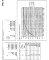
- Table 1 in FIG. 8 discloses some typical values for N and K based on this relationship.
- the Phase Locked Loop (PLL) for drive frequency controller 400 runs with a sampling rate ⁇ of 10us.
- Table 2 disclosed in FIG. 8 includes the values of K for a desired PLL time constant.
- K is a substantial behavior.
- One substantial behavior is that very small changes in K will have a very significant effect on the PLL time constant. This poses computational constraint that must be evaluated carefully.
- equation (11) requires no multiplication only addition, subtraction and a division by a binary number that is implemented as a simple shift.
- 9 bits will be used for the integer portion of y n . This implies an output range of 0 ⁇ y n ⁇ 511 or a frequency as low as 47KHz. The choice of 9 bits imposes no limitation on the high end of the frequency.
- the aforementioned PLL may be implemented in hardware as a custom microchip solution such as ASIC, FPGA, MCM, or alternatively, may also be run as a software module in a microprocessor integrated within, or at least coupled to, battery balancing system 200.
- the PLL may be utilized to determine the fly-back frequency time of charge balancer circuits 310. This time is used to determine 50% of the period for the balancing circuit drive clock time (as shown in FIG. 5 , step 520). Using this balancing circuit drive clock time, the charge balancer circuits 310 should be constantly driven at the most appropriate clock period in view of the natural resonant frequency of charge balancer circuits 310. IV. Compensation for parasitic resistance in a battery monitoring system.
- cell monitoring circuits 330 may be utilized to determine a current voltage level for battery cells 200 in accordance with at least one example out of the scope of the present invention.
- Each battery cell 220 may have its own monitoring circuit 330, and all of these monitoring circuits may be multiplexed together.
- at least one microprocessor may monitor and control the voltage of 24 or more individual battery cells 220.
- the cell monitoring system of the instant example may report a measured charge level in any battery cell 220, at any given time, to the at least one microprocessor.
- the at least one microprocessor may be responsible for a multitude of functions such as generating a balance clock and monitor clock, reporting telemetry information of monitor voltages and battery voltage to another local or remote system (e.g., transmitting the telemetry information to a terrestrial monitoring station), performing automatic internal calibration, supplying power, on/off control, etc.
- the operation of the system may be affected by inaccuracy in battery charge monitoring experienced, for example, due to variations in circuit characteristics caused by the operation of each charge balancer 310. The cause/effect of this inaccuracy is discussed further with regard to FIG. 9A .
- the charge balancing and monitoring system depicted in FIG. 9A is similar to the system of FIG. 3B except that charge balancer 310 is replaced by a simplified representation of the circuit from the perspective of cell monitor 330.
- the share bus voltage is equal to the average voltage of all of the cells.
- Each cell may be connected to the share bus through a resistor (e.g., about 1 ohm) which makes up the greatest part of R_share. This resistor may be used to set a "Transfer Ratio" that determines the magnitude of current when the cells are not balanced. High voltage cells put current into the share bus, and low cells receive current from the share bus. Eventually the cell voltages equalize through this process.
- parasitic (unintentional) resistance R_p may also be present.
- Contributors to R_p may include circuit wiring, secondary DC resistance (DCR) in balancing transformer T1, on-state resistance, or RDS (on), of the transistor Q1, etc. While the use of very large capacitors, very large FET's and/or bigger-gauge electrical conductors is at least one known solution for reducing parasitic resistance in a circuit, the use of such corrective components may be prohibitive due to cost, space, power conservation requirements, etc., especially when the circuit is being implemented in an extremely remote application like a satellite.
- DCR secondary DC resistance
- this parasitic resistance basically increases the 1 ohm summing resistance R_share, which is not usually a problem for the operation of charge balancer 310 in general.
- the parasitic resistance may cause a change in the transfer ratio, which may change the time required to achieve charge balance, but not the final voltage when balance is achieved.
- the summing resistance may, in some cases, be reduced, such that the total resistance (the summing resistor plus the parasitic resistance) equals 1 ohm.
- the parasitic resistance does cause an undesirable error in the measured monitoring voltage. For instance, a monitor voltage error for a particular low cell 220 in a 24 cell battery system 170 may be 287 mV or more, which would be undesirable when trying to render efficient system control.
- the monitoring voltage is taken from the secondary winding of the balancing transformer T1.
- the voltage goes through a Sample/Hold circuit, a low-pass filter, a multiplexer and an A/D Converter as previously discussed with respect to cell monitor 330.
- the digitized monitoring voltages are then sent to the at least one microprocessor for analysis. If all of the cells 220 are close to balance, the balancing currents will be low (e.g., close to zero), and the monitoring errors will be small. However, if one or more 220 cells are out of balance, the balancing current will be high, and large errors may occur due to an IR drop caused by the parasitic resistance R_p. This relationship is graphically depicted in FIG. 6 at 900. As the difference in charge level between battery cells 220 increases, so does the current and parasitic resistance R_p. As a result, the accuracy of monitored cell voltages may decrease.
- At least one example out of the scope of the present invention may include functionality to adjust the raw monitored voltages from each battery cell 220 to account for the error induced by the parasitic resistance.
- V_celli is the actual cell voltage for each cell from 1 to i
- V_moni is the monitored voltage read by cell monitor 330 for each cell from 1 to i
- R_p is the parasitic resistance (e.g., typically 0.3 ohm)
- R_share is the share bus resistance (e.g., typically 1.0 ohm)
- V avg is the share bus voltage.
- V_avg may be measured from the share bus.
- V_mon may be measured by each cell monitor 330, which is routed through multiplexer (MUX) to analog/digital converter (A/D). The digital measurement signal may then be used by the at least one microprocessor in implementing control, reporting telemetry, taking corrective actions, etc.
- MUX multiplexer
- A/D analog/digital converter
- the share bus voltage may be measured or estimated using various techniques. For example, the total battery voltage may be measured and then divided by the number of cells. Alternatively, the average of the individual cell monitor voltages may be computed, or the share bus voltage may be measured directly. An example of the direct measurement of the share bus voltage is disclosed in FIG. 9B .
- Circuit 900 shows another sample and hold circuit 904 similar to cell monitor 330 that may couple (e.g., via 902) the share bus to a multiplexer input. In an exemplary 24-cell battery system 170, a 25th multiplexer input may be used for the share bus.
- a blown fuse may also be problematic when measuring cell voltages.
- Fuse F1 may be used to disconnect a particular cell balancing circuit in the case of a failed shorted cell, which may be a potential failure mode of a lithium-ion cell. In this event, several amps will flow into the shorted cell, and fuse F1 will open.
- the nominal cell voltage may be 4.0 volts
- (R1 + R2) is 1 ohm
- F1 is a 1 amp fuse.
- a fuse F1 opening effectively disconnects a shorted cell from the share bus, and allows balancing to proceed normally among the remaining good cells.
- a normal 24-cell battery system 170 may provide 96 volts. If a cell shorts, a 23-cell battery providing 92 volts remains. A properly designed system may continue to operate with several cells shorted.
- the first two methods rely on the computation of an average voltage, which would in turn require knowledge of the number (N) of participating cell balancing circuits.
- N e.g. the number of active battery cells 200
- the at least one microprocessor must have knowledge of the number of active (or open) fuses. Information related to the number of active cells and/or open fuses may be sent to the at least one microprocessor via monitoring resources in any of the aforementioned circuits.
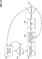
- FIG. 10 discloses a flow chart describing the correction process in accordance with at least one example out of the scope of the present invention.
- cell monitor 330 measures V_mon from a battery cell.
- V_mon may be measured and stored for each cell until all the cells are measured (step 1002).
- each V_cell may be completely calculated before the next raw V_mon value is measured.
- V_avg is measured or calculated in step 1004 (e.g., in accordance with the exemplary methods for obtaining share bus voltage set forth above), and V_cell is then calculated for each battery cell 220 based on each V_mon, V_avg, R_p and R_share in step 1006.
- R_p and R_share may be estimated for each circuit based on the 1 ohm share bus resistor and the empirical testing of circuit behavior, these values may also be measured in real time.
- each V cell may be reported to a control system such as power control system 150. After all the V_cell values have been calculated and reported, the process may again be initiated at step 1008.
- the present example improves upon the state of the art by adding functionality to a power system that was previously not anticipated.
- the present example may improve current battery balancing systems by allowing essential resources to continuously function at optimum efficiency regardless of the impact of "real world" influences on various components within the system.
- the present system provides this functionality by at least monitoring cell voltage levels and adjusting these monitored voltage levels to an actual value for use by at least one processor, which it may utilize these actual voltage levels for control, optimization, telemetry reporting, etc.
- V Battery balancing in low-power applications.
- transformer-coupled cell balancing circuits intended for use with lithium-ion batteries may comprise a number of battery cells connected in series.
- a typical configuration may include 24 cells, with each cell having a nominal voltage of 4.0 volts that may be connected in series to form a 96-volt battery.
- Each cell may be further be connected by a transformer-coupled balancing circuit to a share bus.
- the share bus voltage is equal to the average cell voltage. Charge may then be transferred from the higher (e.g., above average) cells into the share bus, and subsequently into the lower (e.g., below average) cells from the share bus.
- all of the cells in the battery system may eventually equilibrate to the same voltage, and are therefore balanced.
- Transformer-coupled balancing circuits have substantial limitations with respect to small-capacity battery cells. These limitations may include inherent losses in the transformers, which result in a small discharge current taken from the battery cells. Transformer losses may be caused by at least two independent phenomena: 1) core loss, and 2) IR losses resulting from magnetizing current. These losses can cause a cell discharge current of approximately 10 ma at room temperature (e.g., This loss is temperature sensitive, becoming approximately 15 ma at -35 °C and 5 ma at +71 °C). Although these losses may be minimized by careful transformer design, they cannot be eliminated entirely.
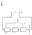
- battery units e.g., 1100 and 1102
- 24 battery units supplying 4 volts each may be connected in series to form a 96-volt battery.
- the battery units may also be electrically coupled to a share bus over which current may flow during charge balancing. While at the outset this system may appear similar to configurations described above, the exemplary balancing circuits that will be described below have been designed in consideration of the requirements and limitations of smaller battery cells.
- FIG. 12A discloses an exemplary battery unit configuration in accordance with at least one example out of the scope of the present invention.
- battery units 1100 and 1102 may each include at least one battery cell 1200. While only single cells have been disclosed for the sake of explanation in this disclosure, the present invention is not only limited to single cells 1200. It may also be possible to have multiple cells 1200 in each battery unit that are connected in parallel to form a "virtual cell.”
- battery units 1100 and 1102 may also include a battery balancing circuit made up of various electronic components. This battery balancing circuit may be incorporated in the housing of battery units 1100 and 1102, which may in turn make the installation and utilization of the battery balancing system easier.
- the present invention may also be implemented as a single chip solution, for example, using customizable chip arrays.
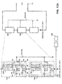
- the balancing circuits do not utilize transformers, although it does have a share bus and it does transfer charge from the high cells to the low cells through the share bus. The difference is that the balancing circuits are capacitor-coupled instead of transformer-coupled.
- Clock 1202 may, for example, provide a square wave output with a duty cycle of 50% and a frequency of 200 KHz.
- Driver IC's U50 are CMOS inverters. In at least one configuration of the instant example, each inverter symbol may actually be six (6) inverters coupled in parallel to provide greater drive capability. Older technology 4000 series devices may be used in this application because they have an operating voltage range of 3V - 15V, and these circuits are configured to operate at the cell voltage, which is nominally 4.0 V. Each cell powers one hex inverter IC U50. All inverters are clocked by the same 200 KHz clock from clock 1202.
- the output from each inverter will be a 200 KHz square wave with a peak-to-peak amplitude equal to the voltage of the cell that powers it.
- All of the inverter outputs may be electrically connected to the share bus through capacitor C54 (e.g., with a value of 0.01 uf).
- the balancing circuit in each battery unit may also use capacitors C50 and C52. Their values may be 0.1 uf and 0.01uf, respectively. However the actual values may vary depending on the application, for example, in terms of the battery voltage.
- CMOS inverter U50 output stages comprise "totem-pole" field-effect transistors (FET), and that in various examples out of the scope of the present invention, current may flow in the reverse direction through an "on" FET. While this may not generally happen in logic circuits, it is an acceptable way for a FET to operate.
- FET field-effect transistor
- This clock unit may reside in a separate housing, or alternatively, may also be incorporated with in the housing of one or more battery units (e.g., 1102).
- the clock may be an inverter based circuit utilizing, for example, inverters U60-U70 as shown in FIG. 12B . These inverters, driven by an oscillator voltage Vosc 1202, may flip back and forth creating a square wave usable with various examples out of the scope of the present invention.
- resisters R60, R62 and R64 may have the following values in ohms: 100 K, 10K and 49.9K, respectively.
- Capacitor C60 may have the value 500 pf, but as stated above, the values of these components may vary depending on the battery system being balanced.
- FIG. 13A An alternate circuit, in accordance with at least one embodiment of the present invention, is shown FIG. 13A .
- inverters U50 have been replaced with discrete N-channel FET's Q80 and Q82, but the concept is basically the same.
- Single line clock 1202 has been replaced with a two-phase clock 1300 to avoid simultaneous conduction (or cross-conduction), in the FET's.
- This particular configuration of the present invention may provide a more controlled on-resistance, which in at least one embodiment may be 10 ohms per channel.
- capacitors C80, C82 and C84 may have the values 0.01 uf, 0.01uf, and 1 uf, respectively.
- Resistors R80, R82 and R84 may have the values in ohms: 10K, 10K and 10.
- D80 and D82 may be diodes in this particular example of the present invention.
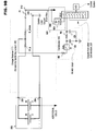
- a dual line clock circuit 1300 used with the balancing circuit of FIG. 13A is now disclosed in FIG. 13B .
- This circuit employs various ICs in order to create a clock signal.
- U106 is a 4022-type logic device
- U102 and U104 are 4013-type logic devices
- U90-U94 and U98 are 4016-type logic devices
- U96 and U100 are 4424-type devices.
- capacitor C90 may have a value of 100pf
- potentiometer P90 may have a variable value of up to 10K ohms. These values are given as an example, and may change depending on the particular application to which embodiments of the present invention may be applied.
- These components work together to create a two phase signal which drives the exemplary circuit, which may in turn facilitate the battery-balancing process previously described with respect to various embodiments of the present invention.
- FIG. 14 discloses timing diagram 1400 that may, in accordance with at least one embodiment of the present invention, be an output from system clock 1300 ( FIG. 13B ) usable in driving the exemplary balancing circuit shown in FIG. 13A .
- Timing diagram 1400 emphasizes an "underlap,” or gap between clock phases (e.g., shown in output signals 1402 and 1404) that prevents the simultaneous conduction of FETs Q80 and Q82.
- flip-flops U102 and U104 in FIG. 14 are shown in a cross-coupled configuration (e.g., the "Q" pin of each device is coupled to the reset, or "R" pin, of the other device). Cross-coupling these devices may, for example, prevent both Q outputs from being high at any time, especially during startup.
- the losses associated with transformers have been eliminated by eliminating the transformers themselves.
- a new loss may occur, instead, due to FET switching losses, but this impact is much smaller in magnitude, and results in a cell discharge current on the order of only 0.1 ma, which may be approximately 100 times smaller than the corresponding loss expected from the use of the transformers.
- the capacitive charge balancing circuit disclosed in FIG. 12A may function over a wide range of frequencies, as it does not contain any components that operate at a certain resonant frequency.
- the transformer-coupled charge balancing circuit of FIG. 3A does have a resonant frequency, and therefore, may require a phase-locked loop (PLL) controller to drive it at this frequency.
- PLL phase-locked loop
- the lack of inherent resonance may be beneficial in certain cases, for example, because the clock may be a simple open-loop circuit that is much less complicated than the PLL.
- Either of the previously discussed circuit embodiments may be constructed on a small circuit board, or as previously mentioned as a monolithic device, and may further be mounted inside the housing of a battery unit (e.g., 1100 and 1102).
- a battery unit e.g. 1100 and 1102
- transformers tend to become helpful and even necessary as current and power become larger.
- the short-falls of using transformers are believed to outweigh the benefits, which is at least one problematic situation solved by the various embodiments of the present invention.
Landscapes
- Engineering & Computer Science (AREA)
- Power Engineering (AREA)
- Manufacturing & Machinery (AREA)
- Chemical & Material Sciences (AREA)
- Chemical Kinetics & Catalysis (AREA)
- Electrochemistry (AREA)
- General Chemical & Material Sciences (AREA)
- Microelectronics & Electronic Packaging (AREA)
- Charge And Discharge Circuits For Batteries Or The Like (AREA)
Claims (2)
- Batteriesystem mit einer Zellenausgleichsschaltung für jede von einer Vielzahl von darin gekoppelten Batteriezellen mit niedriger Kapazität, wobei das Batteriesystem Folgendes umfasst:eine erste Batteriezelle mit niedriger Kapazität (1200);mindestens eine nachfolgende Batteriezelle mit niedriger Kapazität (1200), wobei die niedrige Kapazität für jede Batteriezelle (1200) ungefähr 1 Amperestunde pro Zelle beträgt;eine Zellenausgleichsschaltung für die erste Batteriezelle mit niedriger Kapazität (1200) und eine Zellenausgleichsschaltung für jede der mindestens einen nachfolgenden Batteriezelle mit niedriger Kapazität (1200);einen gemeinsamen Bus;einen Zweiphasentakt (1300), der von einem Oszillator angesteuert wird, um den Ladungsausgleich für jede der Zellenausgleichsschaltungen zu synchronisieren; undwobei jede Zellenausgleichsschaltung Folgendes umfasst:einen ersten Kondensator (C80), wobei ein erster Anschluss des ersten Kondensators (C80) mit einer ersten Leitung des Zweiphasentakts (1300) gekoppelt ist;einen zweiten Kondensator (C82), wobei ein erster Anschluss des zweiten Kondensators (C82) mit einer zweiten Leitung des Zweiphasentakts (1300) gekoppelt ist;einen ersten diskreten N-Kanal-Feldeffekttransistor, FET (Q80); wobei ein Gate des ersten diskreten N-Kanal-FET (Q80) in Reihe mit einem zweiten Anschluss des ersten Kondensators (C80) gekoppelt ist; wobei ein Drain des ersten diskreten N-Kanal-FET (Q80) mit einem positiven Anschluss der jeweiligen Batteriezelle mit niedriger Kapazität (1200) gekoppelt ist;einen zweiten diskreten N-Kanal-FET (Q82); wobei ein Gate des zweiten diskreten N-Kanal-FET (Q82) in Reihe mit einem zweiten Anschluss des zweiten Kondensators (C82) gekoppelt ist; wobei ein Drain des zweiten diskreten N-Kanal-FET (Q82) mit einer Quelle des ersten diskreten N-Kanal-FET (Q80) gekoppelt ist; wobei eine Quelle des zweiten diskreten N-Kanal-FET (Q82) mit einem negativen Anschluss der jeweiligen Batteriezelle mit niedriger Kapazität (1200) gekoppelt und mit einem positiven Anschluss einer nächsten einen der nacheinander verbundenen Batteriezellen mit niedriger Kapazität gekoppelt ist (1200);einen Widerstand (R84), der in Reihe mit dem gemeinsamen Bus geschaltet ist;einen dritten Kondensator (C84), der in Reihe mit dem Widerstand (R84) geschaltet ist;einen zweiten Widerstand (R80) und eine Diode (D80), die parallel zwischen dem Gate des ersten diskreten N-Kanal-FET (Q80) und dem Übergang des dritten Kondensators (C84), der Quelle des ersten diskreten N-Kanals, FET (Q80) und dem Drain des zweiten diskreten N-Kanal-FET (Q82) gekoppelt sind; undeinen dritten Widerstand (R82) und eine zweite Diode (D82), die parallel zwischen dem Gate des zweiten diskreten N-Kanal-FET (Q82) und der Quelle des zweiten diskreten N-Kanal-FET (Q82) gekoppelt sind;wobei der Zweiphasentakt (1300) konfiguriert ist, um eine Zweiphasentaktsignalwellenform auszugeben, die eine Rechteckwelle mit einer Frequenz umfasst, um die diskreten N-Kanal-FETs (Q80, Q82) jeder Ausgleichsschaltung anzusteuern, um die Wellenform mit der Frequenz und mit einer Spitze-Spitze-Amplitude auszugeben, die gleich einer Spannung der jeweiligen Batteriezelle mit niedriger Kapazität (1200) ist;wobei, wenn eine der Batteriezellen mit niedriger Kapazität (1200) eine Spannung aufweist, die niedriger ist als ein Rest der Batteriezellen mit niedriger Kapazität (1200), die Amplitude der Wellenform, die von den diskreten N-Kanal-FETs (Q80, Q82) für die eine Batteriezelle mit niedriger Kapazität (1200) ausgegeben wird, für jede der übrigen Batteriezellen mit niedriger Kapazität (1200) niedriger ist als die Amplitude der Wellenform, die von den diskreten N-Kanal-FETs (Q80, Q82) ausgegeben wird, so dass Strom durch den gemeinsamen Bus von mindestens einem Teil des Restes der Batteriezellen mit niedriger Kapazität (1200) in die eine Batteriezelle mit niedriger Kapazität (1200) fließt;gekennzeichnet durch den Zweiphasentakt (1300), umfassend:eine Logikvorrichtung vom Typ 4022 (U106);eine erste Logikvorrichtung vom Typ 4013 (U102) und eine zweite Logikvorrichtung vom Typ 4013 (U104), die jeweils einen S-Pin und einen C-Pin aufweisen, die mit den jeweiligen Ausgangspins der Logikvorrichtung vom Typ 4022 (U106) verbunden sind;eine erste Logikvorrichtung vom Typ 4016 (U90), eine zweite Logikvorrichtung vom Typ 4016 (U92), eine dritte Logikvorrichtung vom Typ 4016 (U94), die parallel zueinander gekoppelt und mit einem Q-Pin der zweiten Logikvorrichtung vom Typ 4013 gekoppelt ist, wobei die erste Logikvorrichtung vom Typ 4016 (U90) mit einem Spannungspin der Logikvorrichtung vom Typ 4022 (U106) verbunden ist;einen vierten Kondensator (C90), der mit Masse verbunden ist;ein Potentiometer (P90) und eine vierte Logikvorrichtung vom Typ 4016 (U98), die parallel zwischen dem vierten Kondensator (C90) und einem CLK-Pin der Logikvorrichtung vom Typ 4022 (U106) gekoppelt sind;eine erste Logikvorrichtung vom Typ 4424 (U96), die mit dem ersten Kondensator (C80) als die erste Leitung des Zweiphasentakts (1300) gekoppelt und mit einem Q-Pin der ersten Logikvorrichtung vom Typ 4013 (U102) und einem Q-Pin der zweiten Logikvorrichtung vom Typ 4013 (U104) gekoppelt ist;eine zweite Logikvorrichtung vom Typ 4424 (U100), die mit dem zweiten Kondensator (C82) als die zweite Leitung des Zweiphasentakts (1300) gekoppelt und mit einem Q-Pin der ersten Logikvorrichtung vom Typ 4013 (U102) und dem Q-Pin der zweiten Logikvorrichtung vom Typ 4013 (U104) gekoppelt ist; undwobei die Logikvorrichtungen (U90, U92, U94, U96, U98, U100, U102, U104, U106), der vierte Kondensator (C90) und das Potentiometer (P90) konfiguriert sind, um das Zweiphasensignal für den Zweiphasentakt (1300) zu erzeugen, um die Zellenausgleichsschaltungen anzutreiben.
- Batteriesystem nach Anspruch 1, wobei der Zweiphasentakt (1300) konfiguriert ist, um die Rechteckwelle mit einem Tastverhältnis von 50% und einer Frequenz von 200 kHz auszugeben.
Applications Claiming Priority (2)
| Application Number | Priority Date | Filing Date | Title |
|---|---|---|---|
| US12/028,600 US8058844B2 (en) | 2006-05-31 | 2008-02-08 | Low-power battery system |
| PCT/US2008/083635 WO2009099474A1 (en) | 2008-02-08 | 2008-11-14 | Low-power battery system |
Publications (3)
| Publication Number | Publication Date |
|---|---|
| EP2243206A1 EP2243206A1 (de) | 2010-10-27 |
| EP2243206A4 EP2243206A4 (de) | 2016-04-27 |
| EP2243206B1 true EP2243206B1 (de) | 2020-10-21 |
Family
ID=40952382
Family Applications (1)
| Application Number | Title | Priority Date | Filing Date |
|---|---|---|---|
| EP08872241.8A Active EP2243206B1 (de) | 2008-02-08 | 2008-11-14 | Batteriesystem mit niedriger leistung |
Country Status (3)
| Country | Link |
|---|---|
| US (1) | US8058844B2 (de) |
| EP (1) | EP2243206B1 (de) |
| WO (1) | WO2009099474A1 (de) |
Families Citing this family (32)
| Publication number | Priority date | Publication date | Assignee | Title |
|---|---|---|---|---|
| US9088162B2 (en) * | 2008-10-17 | 2015-07-21 | All New Energy Technology Corp. | Hierarchical battery management system |
| DE102009000055A1 (de) * | 2009-01-07 | 2010-07-08 | Robert Bosch Gmbh | Batteriezellen-Balancing |
| US8823323B2 (en) | 2009-04-16 | 2014-09-02 | Valence Technology, Inc. | Batteries, battery systems, battery submodules, battery operational methods, battery system operational methods, battery charging methods, and battery system charging methods |
| DE102009027835A1 (de) | 2009-07-20 | 2011-01-27 | SB LiMotive Company Ltd., Suwon | Hybrides Batteriesystem |
| DE102009027833A1 (de) * | 2009-07-20 | 2011-01-27 | SB LiMotive Company Ltd., Suwon | Serienschaltung von Schaltreglern zur Energieübertragung in Batteriesystemen |
| US8564277B2 (en) | 2009-08-31 | 2013-10-22 | Maxim Integrated Products, Inc. | System for and method of virtual simultaneous sampling with a single ADC core |
| WO2011053951A1 (en) * | 2009-11-02 | 2011-05-05 | Iftron Technologies, Inc. | System and method for both battery charging and load regulation in a single circuit with a single, bidirectional power path |
| JP5567684B2 (ja) * | 2009-12-14 | 2014-08-06 | リーチ インターナショナル コーポレイション | バッテリバランシング回路並びに第1の端子及び第2の端子を有するバッテリの複数のセルに蓄積されたエネルギーのバランシングを行う方法 |
| US8760125B2 (en) * | 2010-02-16 | 2014-06-24 | Blackberry Limited | Power distribution network based on multiple charge storage components |
| HUP1000311A2 (en) | 2010-06-14 | 2012-08-28 | Ferenc Stangl | System and method for charge equalisation and/or charring of electrical energy storing units |
| CN102025177B (zh) * | 2010-12-07 | 2012-11-07 | 中国农业大学 | 蓄电池组电压均衡器 |
| CN103066704A (zh) * | 2011-10-19 | 2013-04-24 | 上海奥威科技开发有限公司 | 基于超级电容器的后备储能模块 |
| TWI501507B (zh) * | 2012-07-13 | 2015-09-21 | 蔡富生 | 藉助於虛擬電池機制來進行電池單元控制之方法與裝置 |
| US9991723B2 (en) | 2012-09-17 | 2018-06-05 | The Boeing Company | Virtual cell method for battery management |
| US9091738B2 (en) * | 2012-10-10 | 2015-07-28 | GM Global Technology Operations LLC | Vehicle battery pack cell voltage determination |
| US9531210B2 (en) * | 2013-01-30 | 2016-12-27 | Semiconductor Components Industries, Llc | Monitor and control module and method |
| US8901888B1 (en) | 2013-07-16 | 2014-12-02 | Christopher V. Beckman | Batteries for optimizing output and charge balance with adjustable, exportable and addressable characteristics |
| US9067504B1 (en) * | 2014-01-14 | 2015-06-30 | Ford Global Technologies, Llc | Perturbative injection for battery parameter identification |
| KR102211867B1 (ko) | 2014-06-09 | 2021-02-04 | 삼성전자주식회사 | 보조 전원 장치 및 그것을 포함하는 불휘발성 메모리 시스템 |
| DE102014214996A1 (de) * | 2014-07-30 | 2016-02-04 | Robert Bosch Gmbh | Verfahren zum Betrieb eines Batteriesystems |
| KR101712244B1 (ko) * | 2014-10-08 | 2017-03-13 | 주식회사 엘지화학 | 엘씨 공진을 이용한 배터리 셀 밸런싱 시스템 및 방법 |
| TWI558084B (zh) * | 2015-04-17 | 2016-11-11 | Bidirectional power control and dual power module parallel return controller | |
| WO2017033398A1 (ja) * | 2015-08-27 | 2017-03-02 | パナソニックIpマネジメント株式会社 | 管理装置および蓄電システム |
| WO2018081912A1 (en) * | 2016-11-07 | 2018-05-11 | Corvus Energy Inc. | Balancing a multi-cell battery |
| CN106655431B (zh) * | 2016-12-21 | 2023-05-12 | 江西佰仕通电子科技有限公司 | 一种自动调节电流充电器电路 |
| US10374440B2 (en) * | 2017-06-22 | 2019-08-06 | Rockwell Collins, Inc. | System and method for supercapacitor charging and balancing |
| US10727550B2 (en) * | 2017-11-13 | 2020-07-28 | Progress Rail Services Corporation | End of train (EOT) system having temperature control for optimized battery charging |
| CN110289656B (zh) * | 2019-07-04 | 2023-05-16 | 大唐恩智浦半导体有限公司 | 电池管理电路及电池模块 |
| US11901532B2 (en) | 2020-12-09 | 2024-02-13 | Vltru Systems Llc | Battery module and battery rack with enhanced fire safety features, and applications thereof |
| KR102848533B1 (ko) * | 2021-06-25 | 2025-08-20 | 주식회사 엘지에너지솔루션 | 배터리 상태 검출 장치 및 배터리 보호 장치 |
| CN113904557B (zh) * | 2021-09-18 | 2022-09-23 | 苏州万可顶钇电源有限公司 | 一种高可靠性双母线互为热备份的自动补偿装置及控制方法 |
| BG113921A (bg) * | 2024-06-21 | 2025-12-30 | "Ендуросат" ЕАД | Система за аналогово балансиране на акумулаторни батерии |
Citations (1)
| Publication number | Priority date | Publication date | Assignee | Title |
|---|---|---|---|---|
| US20040246635A1 (en) * | 2001-10-01 | 2004-12-09 | Koichi Morita | Voltage balance circuit, voltage detective circuit, voltage balancing method, and voltage detecting method |
Family Cites Families (15)
| Publication number | Priority date | Publication date | Assignee | Title |
|---|---|---|---|---|
| DE4422409C2 (de) * | 1994-06-29 | 1996-07-11 | Fraunhofer Ges Forschung | Vorrichtung zum Ladungsaustausch zwischen einer Vielzahl von in Reihe geschalteten Energiespeichern oder -wandlern |
| CA2169706A1 (en) * | 1995-03-03 | 1996-09-04 | Troy Lynn Stockstad | Circuit and method for battery charge control |
| US5710504A (en) * | 1996-05-20 | 1998-01-20 | The Board Of Trustees Of The University Of Illinois | Switched capacitor system for automatic battery equalization |
| US6140800A (en) * | 1999-05-27 | 2000-10-31 | Peterson; William Anders | Autonomous battery equalization circuit |
| JP2001224138A (ja) * | 2000-02-07 | 2001-08-17 | Hitachi Ltd | 蓄電装置及び蓄電器の電圧検出方法 |
| US7378818B2 (en) * | 2002-11-25 | 2008-05-27 | Tiax Llc | Bidirectional power converter for balancing state of charge among series connected electrical energy storage units |
| US6873134B2 (en) * | 2003-07-21 | 2005-03-29 | The Boeing Company | Autonomous battery cell balancing system with integrated voltage monitoring |
| JP2005160169A (ja) * | 2003-11-21 | 2005-06-16 | Texas Instr Japan Ltd | バッテリ保護回路 |
| JP4137842B2 (ja) * | 2004-05-19 | 2008-08-20 | パナソニックEvエナジー株式会社 | 二次電池の容量均等化装置 |
| US7417405B2 (en) * | 2004-10-04 | 2008-08-26 | Black & Decker Inc. | Battery monitoring arrangement having an integrated circuit with logic controller in a battery pack |
| CN101088203B (zh) * | 2004-12-24 | 2010-08-18 | Lg化学株式会社 | 用于在具有多个锂离子电池的电池组中控制电压平衡的系统及其方法 |
| CA2523240C (en) * | 2005-10-11 | 2009-12-08 | Delaware Systems Inc. | Universal battery module and controller therefor |
| US7274170B2 (en) * | 2005-12-02 | 2007-09-25 | Southwest Electronic Energy Corporation | Battery pack control module |
| JP4508145B2 (ja) * | 2006-04-10 | 2010-07-21 | 株式会社デンソー | 組電池の管理装置 |
| US7786701B2 (en) * | 2006-05-31 | 2010-08-31 | Aeroflex Plainview, Inc. | Compensation for parasitic resistance in battery monitoring |
-
2008
- 2008-02-08 US US12/028,600 patent/US8058844B2/en active Active - Reinstated
- 2008-11-14 EP EP08872241.8A patent/EP2243206B1/de active Active
- 2008-11-14 WO PCT/US2008/083635 patent/WO2009099474A1/en not_active Ceased
Patent Citations (1)
| Publication number | Priority date | Publication date | Assignee | Title |
|---|---|---|---|---|
| US20040246635A1 (en) * | 2001-10-01 | 2004-12-09 | Koichi Morita | Voltage balance circuit, voltage detective circuit, voltage balancing method, and voltage detecting method |
Also Published As
| Publication number | Publication date |
|---|---|
| EP2243206A4 (de) | 2016-04-27 |
| WO2009099474A1 (en) | 2009-08-13 |
| US20080185994A1 (en) | 2008-08-07 |
| US8058844B2 (en) | 2011-11-15 |
| EP2243206A1 (de) | 2010-10-27 |
Similar Documents
| Publication | Publication Date | Title |
|---|---|---|
| EP2243206B1 (de) | Batteriesystem mit niedriger leistung | |
| US7786701B2 (en) | Compensation for parasitic resistance in battery monitoring | |
| US7592775B2 (en) | Battery balancing including resonant frequency compensation | |
| US10393818B2 (en) | Systems and methods for characterizing impedance of an energy storage device | |
| Kim et al. | Power electronics-enabled self-X multicell batteries: A design toward smart batteries | |
| CN110462966B (zh) | 智能电池单元以及控制方法和系统 | |
| FI114884B (fi) | Varavirtajärjestelmä | |
| US9231407B2 (en) | Battery system, method of controlling the same, and energy storage system including the battery system | |
| US10297855B2 (en) | Rechargeable multi-cell battery | |
| US9065296B2 (en) | Battery pack, method of measuring voltage of the battery pack, and energy storage system including the battery pack | |
| Koch et al. | Electrochemical impedance spectroscopy for online battery monitoring-power electronics control | |
| US20180241239A1 (en) | Smart cells and control methods and systems | |
| US9912177B2 (en) | Single transformer high-power balancer | |
| Chung et al. | Hybrid energy storage system with active power-mix control in a dual-chemistry battery pack for light electric vehicles | |
| KR20200050950A (ko) | 전기 화학 임피던스 분광을 위한 전기 아키텍처 | |
| DK180691B1 (en) | Controlling on-time of energy modules of an energy storage | |
| WO2017152136A1 (en) | Energy harvester | |
| Li et al. | Predictive control of modular multilevel series/parallel converter for battery systems | |
| Högerl et al. | Battery emulation for battery modular multilevel management (bm3) converters and reconfigurable batteries with series, parallel and bypass function | |
| US20240418792A1 (en) | Battery health determination apparatus and method | |
| Sun et al. | Active battery equalization system based on extended kalman filter and dc-dc bidirectional flyback converter | |
| US20220085651A1 (en) | Low-loss voltage regulator for wireless-charging receivers | |
| Liu et al. | An active equalization circuit based on the share bus for series Li-ion battery | |
| Aspalter et al. | Battery Efficiency and Aging Measurements for Multilevel Battery Energy Storage Systems-DC vs. 100Hz | |
| US20250260241A1 (en) | Techniques for performing soft start for one or more batteries |
Legal Events
| Date | Code | Title | Description |
|---|---|---|---|
| PUAI | Public reference made under article 153(3) epc to a published international application that has entered the european phase |
Free format text: ORIGINAL CODE: 0009012 |
|
| 17P | Request for examination filed |
Effective date: 20100817 |
|
| AK | Designated contracting states |
Kind code of ref document: A1 Designated state(s): AT BE BG CH CY CZ DE DK EE ES FI FR GB GR HR HU IE IS IT LI LT LU LV MC MT NL NO PL PT RO SE SI SK TR |
|
| AX | Request for extension of the european patent |
Extension state: AL BA MK RS |
|
| DAX | Request for extension of the european patent (deleted) | ||
| RA4 | Supplementary search report drawn up and despatched (corrected) |
Effective date: 20160329 |
|
| RIC1 | Information provided on ipc code assigned before grant |
Ipc: H02J 7/00 20060101AFI20160321BHEP |
|
| STAA | Information on the status of an ep patent application or granted ep patent |
Free format text: STATUS: EXAMINATION IS IN PROGRESS |
|
| 17Q | First examination report despatched |
Effective date: 20180102 |
|
| GRAP | Despatch of communication of intention to grant a patent |
Free format text: ORIGINAL CODE: EPIDOSNIGR1 |
|
| STAA | Information on the status of an ep patent application or granted ep patent |
Free format text: STATUS: GRANT OF PATENT IS INTENDED |
|
| RIC1 | Information provided on ipc code assigned before grant |
Ipc: H02J 7/00 20060101AFI20200605BHEP Ipc: H01M 10/42 20060101ALN20200605BHEP |
|
| INTG | Intention to grant announced |
Effective date: 20200629 |
|
| GRAS | Grant fee paid |
Free format text: ORIGINAL CODE: EPIDOSNIGR3 |
|
| GRAA | (expected) grant |
Free format text: ORIGINAL CODE: 0009210 |
|
| STAA | Information on the status of an ep patent application or granted ep patent |
Free format text: STATUS: THE PATENT HAS BEEN GRANTED |
|
| AK | Designated contracting states |
Kind code of ref document: B1 Designated state(s): AT BE BG CH CY CZ DE DK EE ES FI FR GB GR HR HU IE IS IT LI LT LU LV MC MT NL NO PL PT RO SE SI SK TR |
|
| REG | Reference to a national code |
Ref country code: GB Ref legal event code: FG4D |
|
| REG | Reference to a national code |
Ref country code: CH Ref legal event code: EP |
|
| REG | Reference to a national code |
Ref country code: IE Ref legal event code: FG4D |
|
| REG | Reference to a national code |
Ref country code: DE Ref legal event code: R096 Ref document number: 602008063388 Country of ref document: DE |
|
| REG | Reference to a national code |
Ref country code: AT Ref legal event code: REF Ref document number: 1326829 Country of ref document: AT Kind code of ref document: T Effective date: 20201115 |
|
| PGFP | Annual fee paid to national office [announced via postgrant information from national office to epo] |
Ref country code: NL Payment date: 20201125 Year of fee payment: 13 |
|
| PGFP | Annual fee paid to national office [announced via postgrant information from national office to epo] |
Ref country code: AT Payment date: 20201130 Year of fee payment: 13 Ref country code: LU Payment date: 20201127 Year of fee payment: 13 Ref country code: MT Payment date: 20201125 Year of fee payment: 13 Ref country code: DK Payment date: 20201130 Year of fee payment: 13 Ref country code: IE Payment date: 20201127 Year of fee payment: 13 |
|
| PGFP | Annual fee paid to national office [announced via postgrant information from national office to epo] |
Ref country code: BE Payment date: 20201125 Year of fee payment: 13 |
|
| REG | Reference to a national code |
Ref country code: DE Ref legal event code: R081 Ref document number: 602008063388 Country of ref document: DE Owner name: FRONTGRADE TECHNOLOGIES INC. (N.D.GES. DES STA, US Free format text: FORMER OWNER: AEROFLEX PLAINVIEW INC., PLAINVIEW, NY, US Ref country code: DE Ref legal event code: R081 Ref document number: 602008063388 Country of ref document: DE Owner name: COBHAM LONG ISLAND INC, PLAINVIEW, US Free format text: FORMER OWNER: AEROFLEX PLAINVIEW INC., PLAINVIEW, NY, US |
|
| RAP2 | Party data changed (patent owner data changed or rights of a patent transferred) |
Owner name: COBHAM LONG ISLAND INC. |
|
| REG | Reference to a national code |
Ref country code: AT Ref legal event code: MK05 Ref document number: 1326829 Country of ref document: AT Kind code of ref document: T Effective date: 20201021 |
|
| REG | Reference to a national code |
Ref country code: NL Ref legal event code: MP Effective date: 20201021 |
|
| PG25 | Lapsed in a contracting state [announced via postgrant information from national office to epo] |
Ref country code: NO Free format text: LAPSE BECAUSE OF FAILURE TO SUBMIT A TRANSLATION OF THE DESCRIPTION OR TO PAY THE FEE WITHIN THE PRESCRIBED TIME-LIMIT Effective date: 20210121 Ref country code: NL Free format text: LAPSE BECAUSE OF FAILURE TO SUBMIT A TRANSLATION OF THE DESCRIPTION OR TO PAY THE FEE WITHIN THE PRESCRIBED TIME-LIMIT Effective date: 20201021 Ref country code: PT Free format text: LAPSE BECAUSE OF FAILURE TO SUBMIT A TRANSLATION OF THE DESCRIPTION OR TO PAY THE FEE WITHIN THE PRESCRIBED TIME-LIMIT Effective date: 20210222 Ref country code: FI Free format text: LAPSE BECAUSE OF FAILURE TO SUBMIT A TRANSLATION OF THE DESCRIPTION OR TO PAY THE FEE WITHIN THE PRESCRIBED TIME-LIMIT Effective date: 20201021 Ref country code: GR Free format text: LAPSE BECAUSE OF FAILURE TO SUBMIT A TRANSLATION OF THE DESCRIPTION OR TO PAY THE FEE WITHIN THE PRESCRIBED TIME-LIMIT Effective date: 20210122 |
|
| REG | Reference to a national code |
Ref country code: LT Ref legal event code: MG4D |
|
| PG25 | Lapsed in a contracting state [announced via postgrant information from national office to epo] |
Ref country code: LV Free format text: LAPSE BECAUSE OF FAILURE TO SUBMIT A TRANSLATION OF THE DESCRIPTION OR TO PAY THE FEE WITHIN THE PRESCRIBED TIME-LIMIT Effective date: 20201021 Ref country code: SE Free format text: LAPSE BECAUSE OF FAILURE TO SUBMIT A TRANSLATION OF THE DESCRIPTION OR TO PAY THE FEE WITHIN THE PRESCRIBED TIME-LIMIT Effective date: 20201021 Ref country code: PL Free format text: LAPSE BECAUSE OF FAILURE TO SUBMIT A TRANSLATION OF THE DESCRIPTION OR TO PAY THE FEE WITHIN THE PRESCRIBED TIME-LIMIT Effective date: 20201021 Ref country code: ES Free format text: LAPSE BECAUSE OF FAILURE TO SUBMIT A TRANSLATION OF THE DESCRIPTION OR TO PAY THE FEE WITHIN THE PRESCRIBED TIME-LIMIT Effective date: 20201021 Ref country code: IS Free format text: LAPSE BECAUSE OF FAILURE TO SUBMIT A TRANSLATION OF THE DESCRIPTION OR TO PAY THE FEE WITHIN THE PRESCRIBED TIME-LIMIT Effective date: 20210221 Ref country code: BG Free format text: LAPSE BECAUSE OF FAILURE TO SUBMIT A TRANSLATION OF THE DESCRIPTION OR TO PAY THE FEE WITHIN THE PRESCRIBED TIME-LIMIT Effective date: 20210121 Ref country code: AT Free format text: LAPSE BECAUSE OF FAILURE TO SUBMIT A TRANSLATION OF THE DESCRIPTION OR TO PAY THE FEE WITHIN THE PRESCRIBED TIME-LIMIT Effective date: 20201021 |
|
| PG25 | Lapsed in a contracting state [announced via postgrant information from national office to epo] |
Ref country code: HR Free format text: LAPSE BECAUSE OF FAILURE TO SUBMIT A TRANSLATION OF THE DESCRIPTION OR TO PAY THE FEE WITHIN THE PRESCRIBED TIME-LIMIT Effective date: 20201021 |
|
| REG | Reference to a national code |
Ref country code: CH Ref legal event code: PL |
|
| REG | Reference to a national code |
Ref country code: DE Ref legal event code: R097 Ref document number: 602008063388 Country of ref document: DE |
|
| PG25 | Lapsed in a contracting state [announced via postgrant information from national office to epo] |
Ref country code: MC Free format text: LAPSE BECAUSE OF FAILURE TO SUBMIT A TRANSLATION OF THE DESCRIPTION OR TO PAY THE FEE WITHIN THE PRESCRIBED TIME-LIMIT Effective date: 20201021 Ref country code: LT Free format text: LAPSE BECAUSE OF FAILURE TO SUBMIT A TRANSLATION OF THE DESCRIPTION OR TO PAY THE FEE WITHIN THE PRESCRIBED TIME-LIMIT Effective date: 20201021 Ref country code: SK Free format text: LAPSE BECAUSE OF FAILURE TO SUBMIT A TRANSLATION OF THE DESCRIPTION OR TO PAY THE FEE WITHIN THE PRESCRIBED TIME-LIMIT Effective date: 20201021 Ref country code: RO Free format text: LAPSE BECAUSE OF FAILURE TO SUBMIT A TRANSLATION OF THE DESCRIPTION OR TO PAY THE FEE WITHIN THE PRESCRIBED TIME-LIMIT Effective date: 20201021 Ref country code: CZ Free format text: LAPSE BECAUSE OF FAILURE TO SUBMIT A TRANSLATION OF THE DESCRIPTION OR TO PAY THE FEE WITHIN THE PRESCRIBED TIME-LIMIT Effective date: 20201021 Ref country code: EE Free format text: LAPSE BECAUSE OF FAILURE TO SUBMIT A TRANSLATION OF THE DESCRIPTION OR TO PAY THE FEE WITHIN THE PRESCRIBED TIME-LIMIT Effective date: 20201021 |
|
| PLBE | No opposition filed within time limit |
Free format text: ORIGINAL CODE: 0009261 |
|
| STAA | Information on the status of an ep patent application or granted ep patent |
Free format text: STATUS: NO OPPOSITION FILED WITHIN TIME LIMIT |
|
| PG25 | Lapsed in a contracting state [announced via postgrant information from national office to epo] |
Ref country code: LI Free format text: LAPSE BECAUSE OF NON-PAYMENT OF DUE FEES Effective date: 20201130 Ref country code: CH Free format text: LAPSE BECAUSE OF NON-PAYMENT OF DUE FEES Effective date: 20201130 Ref country code: DK Free format text: LAPSE BECAUSE OF FAILURE TO SUBMIT A TRANSLATION OF THE DESCRIPTION OR TO PAY THE FEE WITHIN THE PRESCRIBED TIME-LIMIT Effective date: 20201021 |
|
| 26N | No opposition filed |
Effective date: 20210722 |
|
| PG25 | Lapsed in a contracting state [announced via postgrant information from national office to epo] |
Ref country code: SI Free format text: LAPSE BECAUSE OF FAILURE TO SUBMIT A TRANSLATION OF THE DESCRIPTION OR TO PAY THE FEE WITHIN THE PRESCRIBED TIME-LIMIT Effective date: 20201021 |
|
| PG25 | Lapsed in a contracting state [announced via postgrant information from national office to epo] |
Ref country code: IS Free format text: LAPSE BECAUSE OF FAILURE TO SUBMIT A TRANSLATION OF THE DESCRIPTION OR TO PAY THE FEE WITHIN THE PRESCRIBED TIME-LIMIT Effective date: 20210221 Ref country code: TR Free format text: LAPSE BECAUSE OF FAILURE TO SUBMIT A TRANSLATION OF THE DESCRIPTION OR TO PAY THE FEE WITHIN THE PRESCRIBED TIME-LIMIT Effective date: 20201021 Ref country code: CY Free format text: LAPSE BECAUSE OF FAILURE TO SUBMIT A TRANSLATION OF THE DESCRIPTION OR TO PAY THE FEE WITHIN THE PRESCRIBED TIME-LIMIT Effective date: 20201021 |
|
| PG25 | Lapsed in a contracting state [announced via postgrant information from national office to epo] |
Ref country code: LU Free format text: LAPSE BECAUSE OF NON-PAYMENT OF DUE FEES Effective date: 20211114 Ref country code: BE Free format text: LAPSE BECAUSE OF NON-PAYMENT OF DUE FEES Effective date: 20211130 |
|
| REG | Reference to a national code |
Ref country code: BE Ref legal event code: MM Effective date: 20211130 |
|
| PG25 | Lapsed in a contracting state [announced via postgrant information from national office to epo] |
Ref country code: IE Free format text: LAPSE BECAUSE OF NON-PAYMENT OF DUE FEES Effective date: 20211114 |
|
| REG | Reference to a national code |
Ref country code: GB Ref legal event code: 732E Free format text: REGISTERED BETWEEN 20240502 AND 20240508 |
|
| PG25 | Lapsed in a contracting state [announced via postgrant information from national office to epo] |
Ref country code: MT Free format text: LAPSE BECAUSE OF NON-PAYMENT OF DUE FEES Effective date: 20211114 |
|
| REG | Reference to a national code |
Ref country code: DE Ref legal event code: R081 Ref document number: 602008063388 Country of ref document: DE Owner name: FRONTGRADE TECHNOLOGIES INC. (N.D.GES. DES STA, US Free format text: FORMER OWNER: COBHAM LONG ISLAND INC, PLAINVIEW, NY, US |
|
| PGFP | Annual fee paid to national office [announced via postgrant information from national office to epo] |
Ref country code: DE Payment date: 20251119 Year of fee payment: 18 |
|
| PGFP | Annual fee paid to national office [announced via postgrant information from national office to epo] |
Ref country code: GB Payment date: 20251121 Year of fee payment: 18 |
|
| PGFP | Annual fee paid to national office [announced via postgrant information from national office to epo] |
Ref country code: IT Payment date: 20251125 Year of fee payment: 18 |
|
| PGFP | Annual fee paid to national office [announced via postgrant information from national office to epo] |
Ref country code: FR Payment date: 20251121 Year of fee payment: 18 |