EP2244090B1 - Dispositif de détection d'un gaz ou d'un mélange de gaz et procédé de fabrication de celui-ci - Google Patents
Dispositif de détection d'un gaz ou d'un mélange de gaz et procédé de fabrication de celui-ci Download PDFInfo
- Publication number
- EP2244090B1 EP2244090B1 EP10004218.3A EP10004218A EP2244090B1 EP 2244090 B1 EP2244090 B1 EP 2244090B1 EP 10004218 A EP10004218 A EP 10004218A EP 2244090 B1 EP2244090 B1 EP 2244090B1
- Authority
- EP
- European Patent Office
- Prior art keywords
- gas
- semiconductor substrate
- sensitive layer
- channel region
- semiconductor chip
- Prior art date
- Legal status (The legal status is an assumption and is not a legal conclusion. Google has not performed a legal analysis and makes no representation as to the accuracy of the status listed.)
- Not-in-force
Links
Images



Classifications
-
- G—PHYSICS
- G01—MEASURING; TESTING
- G01N—INVESTIGATING OR ANALYSING MATERIALS BY DETERMINING THEIR CHEMICAL OR PHYSICAL PROPERTIES
- G01N27/00—Investigating or analysing materials by the use of electric, electrochemical, or magnetic means
- G01N27/26—Investigating or analysing materials by the use of electric, electrochemical, or magnetic means by investigating electrochemical variables; by using electrolysis or electrophoresis
- G01N27/403—Cells and electrode assemblies
- G01N27/414—Ion-sensitive or chemical field-effect transistors, i.e. ISFETS or CHEMFETS
- G01N27/4141—Ion-sensitive or chemical field-effect transistors, i.e. ISFETS or CHEMFETS specially adapted for gases
- G01N27/4143—Air gap between gate and channel, i.e. suspended gate [SG] FETs
Definitions
- the invention relates to a device for detecting a gas or gas mixture, comprising a first and a second gas sensor, wherein the first gas sensor is a MOSFET having a first source, a first drain, a first channel region located between them and a capacitive to the first channel region coupled first gas-sensitive layer containing palladium and reacts with a change in their work function on a change in the concentration of the gas to be detected, wherein the second gas sensor in a semiconductor substrate has a second source, a second drain and between them a second channel region via an air gap is capacitively coupled to a suspended gate comprising a second gas-sensitive layer which reacts to a change in the concentration of the gas to be detected with a change in its work function, wherein the second gas-sensitive layer is arranged on a carrier layer and facing the air gap. Moreover, the invention relates to a method for producing a device for detecting a gas or gas mixture.
- Such a device is off EP 1 620 717 B1 known. It has two different types of gas sensors.
- a first gas sensor is designed as a suspended gate field effect transistor (SGFET) and a second gas sensor as a so-called Lundström FET.
- the Lundstrom FET has a first transistor well of a first charge carrier type, which is integrated in the semiconductor substrate of a semiconductor chip.
- a first source and a first drain are inserted, which are doped with charge carriers of a second charge carrier type.
- a first channel region is formed, on which a dielectric layer is arranged.
- the dielectric layer is coated with a first gas-sensitive layer containing palladium which reacts to a change in the concentration of the gas to be detected with a change in its work function. This change influences, via the first channel region, a first current flowing between the first source and the first drain.
- the SGFET has a second transistor well of the first charge carrier type, which is monolithically integrated in the semiconductor substrate next to the first transistor well with a lateral distance to it.
- a second source and a second drain are inserted, which are doped with charge carriers of the second charge carrier type.
- a second channel region is formed, which capacitively coupled via an air gap to a Suspended Gate.
- the suspended gate is arranged on a carrier layer bridging the second channel region and has a second gas-sensitive layer facing the second channel region.
- the second gas-sensitive layer contains palladium and / or platinum and responds to a change in the concentration of the gas to be detected with a change in its work function. This change influences a second current flowing between the second source and the second drain via the second channel region.
- the SGFET and the Lundström FET are connected to an evaluation device integrated in the semiconductor substrate, which evaluates the measurement signals of both types of gas sensors for the detection of the gas or gas mixture.
- the device has proved to be particularly advantageous in practice because the Lundström FET and the SGFET have different gas detection properties, and because the gas or gas mixture is detected with much greater accuracy by the evaluation of the measurement signals of both types of gas sensors can be considered with a device that has only one type of gas sensors.
- a disadvantage of the device is that under certain operating conditions, especially when measuring very high gas concentrations, at high temperature and high humidity, an irreversible change in the SGFET can occur. By this change, the measurement accuracy of the device can decrease.
- Another disadvantage is that the device has a relatively large chip area compared to a device which has only a single gas sensor. The manufacture of the device is therefore associated with corresponding costs.
- the object is to provide a method for producing a device for detecting a gas or gas mixture, which allows compact dimensions and in which an irreversible change of the SGFET is largely avoided.
- the invention is based on the finding that during the integration of both gas sensors into the same semiconductor chip in the process steps required for the production of the first gas sensor (Lundström-FET), in particular during application and / or structuring of the first gas-sensitive layer containing the palladium, also the chip surface in the region of the second gas sensor (SGFET) is changed.
- SGFET second gas sensor
- the second channel region can therefore also be coupled capacitively via the gate electrode and the sensor electrode connected thereto via the air gap to the second gas-sensitive layer (CCFET). This makes it possible to arrange the second channel region laterally next to the second gas-sensitive layer.
- the first semiconductor substrate is coated over its entire surface with the material containing the palladium of the first gas-sensitive layer, and then the material is removed from the surface of the first semiconductor substrate at locations where the first gas-sensitive layer should not be.
- the first gas-sensitive layer can be structured inexpensively.
- a structure is produced to which the material of the first gas-sensitive layer adheres better than to a surface region of the first semiconductor substrate which does not have this structure, and after coating the first semiconductor substrate with the material thereof in the non-structural surface area is removed from the surface region.
- the removal of the material can be carried out in a simple manner with the aid of ultrasound.
- the material can be clamped before and / or during the ultrasound treatment by bringing it into contact with hydrogen, so that it better separates from the first semiconductor substrate at those points where the first gas-sensitive layer should not be.
- the areal removal of the material preferably takes place by backside grinding of the first semiconductor substrate.
- an evaluation device is integrated in the second semiconductor substrate, which is connected via bonding wires or the like electrical connections to the first drain and / or the first source and via interconnects to the second drain and / or the second source.
- the device is then even cheaper to produce with compact dimensions.
- a further evaluation device is integrated into the first semiconductor substrate, and that the first-mentioned evaluation device cooperates with the further evaluation device.
- the evaluation device integrated in the second semiconductor substrate can also be connected indirectly to the first drain and / or the first source via the evaluation device integrated in the first semiconductor substrate.
- the device can be manufactured inexpensively in mass production.
- the singulation of the semiconductor chips can be done by sawing.
- At least one electrical heating element and / or at least one temperature sensor are integrated on the first semiconductor substrate.
- the heating element and / or the temperature sensor can then be produced practically without additional effort.
- For heating the first gas-sensitive layer only the first, preferably smaller semiconductor chip needs to be heated. Compared to a device in which the heating element is integrated in the second semiconductor chip, this heating energy can be saved.
- the above-mentioned object is achieved in that the carrier layer is formed by a further semiconductor substrate, and in that the first gas sensor is integrated into the front side of the second semiconductor substrate facing away from the air gap.
- the two semiconductor substrates namely that for the first gas sensor and that for the drain, the source, the channel region and optionally the gate electrode and the sensor electrode of the second gas sensor, are thus stacked on top of each other.
- the device thereby enables very compact dimensions, which correspond approximately to those of a conventional SGFET or CCFET. Since the first gas sensor is arranged on a different substrate than the drain, the source and the channel region of the second gas sensor, the corresponding semiconductor chips can be processed separately from one another. This avoids that the surface of the other semiconductor chip is changed by the production of the semiconductor chip having the first gas sensor and / or comes into contact with the palladium of the first gas-sensitive layer.
- the second gas sensor can be configured as SGFET, in which the air gap is formed between the second channel region and the second gas-sensitive layer.
- the second drain, the second source and the second channel region are preferably arranged below the carrier layer of the suspended gate.
- the second gas sensor may also be a CCFET having a gate electrode arranged on the second channel region and a sensor electrode spaced laterally therefrom, which is electrically connected to the gate electrode, the air gap being formed between the sensor electrode and the second gas-sensitive layer.
- the second drain, the second source, the second channel region and the gate electrode may possibly also be arranged laterally next to a subregion of the second semiconductor substrate which is covered by the carrier layer of the suspended gate.
- the first gas sensor and the second gas sensor may be connected to an evaluation device which is designed such that it evaluates the measurement signals of the first gas sensor and the second gas sensor for the detection of the gas or gas mixture, wherein the Evaluation device is preferably integrated in the semiconductor substrate of the second gas sensor.
- the electrical connection between the first gas sensor and the evaluation device can take place via first and second interconnects, the first interconnects having connection contacts arranged on the semiconductor substrate of the first gas sensor and the second interconnects having the second drain, the second source and the second channel region receiving contact semiconductor substrate arranged mating contacts are connected.
- the mating contacts are each connected via a bonding wire with a connection contact assigned to them.
- the gas to be detected is preferably hydrogen gas.
- the device may also be used to measure ammonia or nitrogen dioxide or a mixture of the gases mentioned.
- At least one electrical heating element and / or at least one temperature sensor is integrated into the further semiconductor substrate.
- the first semiconductor chip having the first gas sensor then needs to be heated, which may have a small chip area than the second semiconductor chip having the second gas sensor. As a result, heating energy can be saved.
- the first gas-sensitive layer may consist of palladium and / or platinum and / or an alloy containing at least one of these metals.
- a method for producing a device 1 which has a Lundström-FET 2 and an SGFET 3 for the detection of a gas or gas mixture, first a first semiconductor chip 4 and a second semiconductor chip 5 are produced.
- a first wafer is provided for producing a plurality of first semiconductor chips 4, which has a first semiconductor substrate 6 only partially shown in the drawing.
- a first transistor well 7 which is doped with charge carriers of a first charge carrier type, is introduced into the front side of the first semiconductor substrate 6 for each first semiconductor chip 4.
- the first transistor wells 7 can be generated, for example, by bombardment of the first semiconductor substrate 6 with ions.
- a first drain 8 and a first source 9 are introduced in a further method step, which are doped with charge carriers of a second charge carrier type (US Pat. Fig. 1 B) , Between the first drain 8 and the first source 9, a first channel region 10 is formed in each case. On the first channel regions 10, a dielectric insulation layer not shown in detail in the drawing is applied.
- the Front side of the semiconductor substrate 6 over the entire surface with palladium coated ( Fig. 1C)
- the palladium can be applied to the semiconductor substrate 6 by electroless plating, for example.
- the palladium is removed from the semiconductor substrate 6 at the locations where the first gas-sensitive layers 11 should not be ( Fig. 1 D) , In the first wafer now one of the number of first semiconductor chips 4 to be produced corresponding number Lundström FET 2 is integrated.
- the back of the first wafer facing away from the first gas-sensitive layers 11 is freed of any layers which may have formed during the production of the Lundström-FET 2 by removing material from the backside of the wafer in a layer near the surface.
- the material can be removed by a grinding process.
- a second gas-sensitive layer 12 is applied over the entire surface of the first gas-sensitive layer 11 facing away from the back of the first wafer, which reacts to a change in the concentration of the gas to be detected with a change in their work function ( Fig. 1 E) ,
- the second gas-sensitive layer may consist of platinum, for example.
- the individual first semiconductor chips 4 are separated out of the first wafer by, for example, sawing it along predetermined separation lines and / or breaking it.
- a second wafer is provided for producing a plurality of second semiconductor chips 5, which has a second semiconductor substrate 13 only partially shown in the drawing
- a second transistor well 14 which is doped with charge carriers of the first charge carrier type, is introduced in each case for each second semiconductor chip 5.
- the second transistor wells 14 may be generated, for example, by bombardment of the second semiconductor substrate 13 with ions.
- a second drain 15 and a second source 16 which are doped with charge carriers of the second charge carrier type, are introduced in a further method step ( Fig. 2B ). Between the second drain 15 and the second source 16, a second channel region 17 is formed in each case.
- intermediate layers 18 are applied, which protrude over the surface of the second semiconductor substrate 13.
- the individual second semiconductor chips 5 are separated out of the second wafer by, for example, sawing it along predetermined separation lines and / or breaking it.
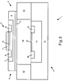
- a first semiconductor chip 4 and a second semiconductor chip 5 are positioned relative to one another such that the second gas-sensitive layer 12 provided on the first semiconductor chip 4 faces the second channel region 17 and is capacitively coupled thereto via an air gap 19 (FIG. Fig. 3 ).
- the second gas-sensitive layer 12 comes to the intermediate layers 18 to the plant.
- the first semiconductor chip 4 and the second semiconductor chip 5 are connected to each other by a bonding step and fixed relative to each other, so that the two semiconductor chips 4, 5 form the SGFET 3.
- first drain 8 and the first source 9 are connected via first conductor tracks with first terminal contacts not shown in detail in the drawing.
- the second semiconductor chip 5 has a mating contact which is connected via a bonding wire to a connection contact assigned to it.
- the mating contacts are connected via second interconnects with an evaluation device not shown in detail in the drawing, which is integrated into the second semiconductor chip 5. Via further strip conductors, the evaluation device is connected to the second drain 15 and the second source 16.
- the device 1 may also comprise a Lundström FET 2 and a CCFET 20, which are arranged one above the other.
- the method steps for the production of the first semiconductor chip 4 are identical to those of the method for producing a device comprising a Lundström-FET 2 and a SGFET 3, which is why with respect to these method steps on the Fig. 1A to 1E and the associated description is referenced.
- a second wafer is provided which has a second semiconductor substrate 13' only partially shown in the drawing.
- a second transistor well 14 ' which is doped with charge carriers of the first charge carrier type, is introduced into the front side of the second semiconductor substrate 13' for each second semiconductor chip 5 '.
- the second transistor wells 14 ' can be generated, for example, by bombardment of the second semiconductor substrate 1 3' with ions.
- a second drain 15' and a second source 16 ' which are doped with charge carriers of the second charge carrier type, are introduced ( Fig. 4B ). Between the second drain 15 'and the second source 16' in each case a second channel region 17 'is formed.
- the arrangement thus obtained is coated with an intermediate layer 18 ', to which for each second semiconductor chip 5' in each case one of the gate electrode 21 of the respective second semiconductor chip 5 'spaced sensor electrode 22 is applied, electrically via a conductor track with her associated gate electrode 21 is connected.
- Fig. 4D is It can be seen that the intermediate layer 18 'has projections on both sides of the sensor electrode 22 which project beyond the sensor electrode 22.
- the individual second semiconductor chips 5 ' are separated out of the second wafer, for example, by sawing it and / or breaking it along predetermined separation lines.
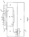
- a first semiconductor chip 4 and a second semiconductor chip 5 ' are positioned relative to one another such that the second gas-sensitive layer 12 provided on the first semiconductor chip 4 faces the sensor electrode 22 and is capacitively coupled thereto via an air gap 19' (FIG. Fig. 5 ).
- the second gas-sensitive layer 12 comes to the supernatants of the intermediate layer 18 'to the plant.
- the first semiconductor chip 4 and the second semiconductor chip 5 ' are connected to each other by a bonding step and fixed relative to each other, so that the two semiconductor chips 4, 5' form the CCFET 3.
- the second semiconductor chip 5 ' For each first connection contact of the first semiconductor chip 4, the second semiconductor chip 5 'has a mating contact, which is connected via a bonding wire to a connection contact.
- the mating contacts are connected via second interconnects to an evaluation device not shown in detail in the drawing, which is integrated in the second semiconductor chip 5 '. Via further strip conductors, the evaluation device is connected to the second drain 15 'and the second source 16'.
- Fig. 5 is still recognizable that the second channel region 17 'in the second semiconductor substrate 13' laterally adjacent to the second gas-sensitive layer 12 and laterally adjacent to the air gap 19 is arranged.
- the second semiconductor chip 5 ' has a larger chip area than the first semiconductor chip 4 and protrudes laterally beyond it.
Landscapes
- Life Sciences & Earth Sciences (AREA)
- Chemical & Material Sciences (AREA)
- Health & Medical Sciences (AREA)
- Physics & Mathematics (AREA)
- Molecular Biology (AREA)
- Microelectronics & Electronic Packaging (AREA)
- Chemical Kinetics & Catalysis (AREA)
- Electrochemistry (AREA)
- Engineering & Computer Science (AREA)
- Analytical Chemistry (AREA)
- Biochemistry (AREA)
- General Health & Medical Sciences (AREA)
- General Physics & Mathematics (AREA)
- Immunology (AREA)
- Pathology (AREA)
- Investigating Or Analyzing Materials By The Use Of Electric Means (AREA)
Claims (15)
- Procédé de fabrication d'un dispositif (1) pour la détection d'un gaz ou d'un mélange de gaz,- dans lequel on fabrique une première puce à semi-conducteur (4), par le fait qu'- on prépare un premier substrat semi-conducteur (6),- on forme sur la face avant du premier substrat semi-conducteur (6) un premier drain (8), une première source (9), une première région de canal (10) se trouvant entre ceux-ci et une première couche sensible au gaz (11) qui contient du palladium et qui réagit par une variation de son travail de sortie à une variation de la concentration du gaz à détecter,- dans lequel on agence la première région de canal (10) et la première couche sensible au gaz (11) de telle manière que la première couche sensible au gaz (11) soit couplée de façon capacitive à la première région de canal (10),- on recouvre la face arrière du premier substrat semi-conducteur (6) avec une deuxième couche sensible au gaz (12) qui réagit par une variation de son travail de sortie à une variation de la concentration du gaz à détecter,- dans lequel on fabrique une deuxième puce à semi-conducteur (5), par le fait que- on prépare un deuxième substrat semi-conducteur (13),- sur lequel on forme un deuxième drain (15), une deuxième source (16) et une deuxième région de canal (17) se trouvant entre ceux-ci,dans lequel on positionne la première puce à semi-conducteur (4) et la deuxième puce à semi-conducteur (5) l'une par rapport à l'autre de telle manière que la deuxième couche sensible au gaz (12) soit tournée vers la deuxième région de canal (17) et soit couplée à celle-ci de façon capacitive par l'intermédiaire d'un entrefer (18) et dans lequel on fixe la première puce à semi-conducteur (4) et la deuxième puce à semi-conducteur (5) dans cette position l'une par rapport à l'autre.
- Procédé de fabrication d'un dispositif (1) pour la détection d'un gaz ou d'un mélange de gaz,- dans lequel on fabrique une première puce à semi-conducteur (4), par le fait qu'- on prépare un premier substrat semi-conducteur (6),- on forme sur la face avant du premier substrat semi-conducteur un premier drain (8), une première source (9), une première région de canal (10) se trouvant entre ceux-ci et une première couche sensible au gaz (11) qui contient du palladium et qui réagit par une variation de son travail de sortie à une variation de la concentration du gaz à détecter,- dans lequel on agence la première région de canal (10) et la première couche sensible au gaz (11) de telle manière que la première couche sensible au gaz (11) soit couplée de façon capacitive à la première région de canal (10),- on recouvre la face arrière du premier substrat semi-conducteur (6) avec une deuxième couche sensible au gaz (12) qui réagit par une variation de son travail de sortie à une variation de la concentration du gaz à détecter,- dans lequel on fabrique une deuxième puce à semi-conducteur (5'), par le fait que- on prépare un deuxième substrat semi-conducteur (13'),- sur lequel on forme un deuxième drain (15'), une deuxième source (16') et une deuxième région de canal (17') se trouvant entre ceux-ci,- on forme sur celui-ci une électrode de grille (21) couplée de façon capacitive à la deuxième région de canal (17') et électriquement isolée de la deuxième région de canal (17') et une électrode de capteur (22) espacée latéralement de l'électrode de grille (21) qui est électriquement reliée à l'électrode de grille (21),dans lequel on positionne la première puce à semi-conducteur (4) et la deuxième puce à semi-conducteur (5') l'une par rapport à l'autre de telle manière que la deuxième couche sensible au gaz (12) soit tournée vers l'électrode de capteur (22) et soit couplée à celle-ci de façon capacitive par l'intermédiaire d'un entrefer (19'), et dans lequel on fixe la première puce à semi-conducteur (4) et la deuxième puce à semi-conducteur (5') dans cette position l'une par rapport à l'autre.
- Procédé selon la revendication 1 ou 2, caractérisé en ce que l'on recouvre le premier substrat semi-conducteur (6) sur toute la surface avec le matériau contenant du palladium de la première couche sensible au gaz (12) et on enlève ensuite le matériau de la surface du premier substrat semi-conducteur (6) aux endroits où la première couche sensible au gaz (11) ne doit pas être présente.
- Procédé selon la revendication 3, caractérisé en ce qu'avant de recouvrir le premier substrat semi-conducteur (6) avec la première couche sensible au gaz (11), on forme sur la première région de canal (10) une structure sur laquelle le matériau de la première couche sensible au gaz (11) adhère mieux que sur une région de surface du premier substrat semi-conducteur (6) qui ne présente pas cette structure et en ce qu'après le recouvrement du premier substrat semi-conducteur (6) avec le matériau, on enlève celui-ci de la région de surface dans la région de surface qui ne présente pas la structure.
- Procédé selon l'une quelconque des revendications 1 à 4, caractérisé en ce qu'après le recouvrement du premier substrat semi-conducteur (6) avec la première couche sensible au gaz (11), on enlève du matériau en surface sur la face arrière du premier substrat semi-conducteur (6) et en ce que l'on recouvre ensuite la face arrière avec la deuxième couche sensible au gaz (12).
- Procédé selon l'une quelconque des revendications 1 à 5, caractérisé en ce que l'on intègre dans le deuxième substrat semi-conducteur (13, 13') un dispositif d'évaluation, que l'on relie par des fils de liaison ou des raccordements électriques analogues au premier drain (8) et/ou à la première source (9) ainsi que par des pistes conductrices au deuxième drain (15, 15') et/ou à la deuxième source (16, 16').
- Procédé selon l'une quelconque des revendications 1 à 6, caractérisé en ce que l'on produit une multiplicité de la première puce à semi-conducteur (4) sur une première galette et on isole ensuite les premières puces à semi-conducteur (4) en ce que l'on produit une multiplicité des deuxièmes puces à semi-conducteur (5, 5') sur une deuxième galette et on isole ensuite les deuxièmes puces à semi-conducteur (5, 5') et en ce que l'on positionne ensuite les premières puces à semi-conducteur (4) et les deuxièmes puces à semi-conducteur (5, 5') respectivement les unes par rapport aux autres et on les relie les unes aux autres.
- Procédé selon l'une quelconque des revendications 1 à 7, caractérisé en ce que l'on intègre sur le premier substrat semi-conducteur (6) au moins un élément chauffant électrique et/ou au moins un détecteur de température.
- Dispositif (1) pour la détection d'un gaz ou d'un mélange de gaz avec un premier et un deuxième détecteur de gaz dans lequel le premier détecteur de gaz est un MOSFET, qui présente une première source (9), un premier drain (8), une première région de canal (10) se trouvant entre ceux-ci et une première couche sensible au gaz (11) couplée de façon capacitive à la première région de canal (10), qui contient du palladium et qui réagit par une variation de son travail de sortie à une variation de la concentration du gaz à détecter, dans lequel le deuxième détecteur de gaz comprend dans un substrat semi-conducteur (13) une deuxième source (16, 16'), un deuxième drain (17, 17') et, entre ceux-ci, une deuxième région de canal (17, 17'), qui est couplée de façon capacitive par l'intermédiaire d'un entrefer (19, 19') à une grille suspendue qui présente une deuxième couche sensible au gaz (12), qui réagit par une variation de son travail de sortie à une variation de la concentration du gaz à détecter dans lequel la deuxième couche sensible au gaz (12) est disposée sur une couche de support et est tournée vers l'entrefer (19, 19'), caractérisé en ce que la couche de support est formée par un autre substrat semi-conducteur (6) et en ce que le premier détecteur de gaz est intégré dans la face avant de l'autre substrat semi-conducteur (6) détournée de l'entrefer (19, 19').
- Dispositif (1) selon la revendication 9, caractérisé en ce que le deuxième détecteur de gaz est un SGFET dans lequel l'entrefer (19) est formé entre la deuxième région de canal (17) et la deuxième couche sensible au gaz (12).
- Dispositif (1) selon la revendication 9, caractérisé en ce que le deuxième détecteur de gaz est un CCFET qui présente une électrode de grille (21) agencée sur la deuxième région de canal (17') et une électrode de capteur (22) espacée latéralement de celle-ci qui est électriquement reliée à l'électrode de grille (21) dans lequel l'entrefer (19') est formé entre l'électrode de capteur (22) et la deuxième couche sensible au gaz (12).
- Dispositif (1) selon l'une quelconque des revendications 9 à 11, caractérisé en ce que le premier détecteur de gaz et le deuxième détecteur de gaz sont reliés à un dispositif d'évaluation qui est configuré de telle manière que, pour la détection du gaz ou du mélange de gaz, il évalue les signaux de mesure du premier détecteur de gaz et du deuxième détecteur de gaz et en ce que le dispositif d'évaluation est de préférence intégré dans le substrat semi-conducteur (13) du deuxième détecteur de gaz.
- Dispositif (1) selon l'une quelconque des revendications 9 à 12, caractérisé en ce que le gaz est l'hydrogène gazeux, l'ammoniac et/ou le dioxyde d'azote ou le mélange de gaz contient de l'hydrogène gazeux, de l'ammoniac et/ou du dioxyde d'azote.
- Dispositif (1) selon l'une quelconque des revendications 9 à 13, caractérisé en ce que la première couche sensible au gaz (11) se compose de palladium et/ou de platine et/ou d'un alliage contenant au moins l'un de ces métaux.
- Dispositif (1) selon l'une quelconque des revendications 8 à 13, caractérisé en ce qu'au moins un élément chauffant électrique et/ou au moins un détecteur de température est intégré dans l'autre substrat semi-conducteur (6).
Applications Claiming Priority (1)
| Application Number | Priority Date | Filing Date | Title |
|---|---|---|---|
| DE102009018364A DE102009018364A1 (de) | 2009-04-23 | 2009-04-23 | Vorrichtung zur Detektion eines Gases oder Gasgemisches und Verfahren zum Herstellen einer solchen |
Publications (2)
| Publication Number | Publication Date |
|---|---|
| EP2244090A1 EP2244090A1 (fr) | 2010-10-27 |
| EP2244090B1 true EP2244090B1 (fr) | 2016-03-23 |
Family
ID=42341757
Family Applications (1)
| Application Number | Title | Priority Date | Filing Date |
|---|---|---|---|
| EP10004218.3A Not-in-force EP2244090B1 (fr) | 2009-04-23 | 2010-04-21 | Dispositif de détection d'un gaz ou d'un mélange de gaz et procédé de fabrication de celui-ci |
Country Status (3)
| Country | Link |
|---|---|
| US (1) | US8242545B2 (fr) |
| EP (1) | EP2244090B1 (fr) |
| DE (1) | DE102009018364A1 (fr) |
Families Citing this family (7)
| Publication number | Priority date | Publication date | Assignee | Title |
|---|---|---|---|---|
| EP2799852A1 (fr) * | 2013-04-29 | 2014-11-05 | Stichting IMEC Nederland | Capteur à base 2DE et dispositif pour détecter un signal ECG |
| DE102014016394B4 (de) * | 2014-11-07 | 2022-09-08 | Dräger Safety AG & Co. KGaA | Gassensor und Gasmessgerät zum Nachweis volatiler organischer Verbindungen |
| JP6005204B1 (ja) * | 2015-03-30 | 2016-10-12 | 日本写真印刷株式会社 | 薄膜トランジスタの製造方法、および薄膜トランジスタ |
| JP6639566B2 (ja) * | 2018-06-08 | 2020-02-05 | オムロン株式会社 | マイクロホットプレート及びmemsガスセンサ |
| US10770573B2 (en) * | 2018-09-20 | 2020-09-08 | Tower Semiconductor Ltd. | Apparatus, system and method of an electrostatically formed nanowire (EFN) |
| CN116087148B (zh) * | 2022-12-18 | 2025-08-19 | 湖州学院 | 一种基于法布里-玻罗谐振腔的甲烷探测系统 |
| TWI892787B (zh) * | 2024-08-06 | 2025-08-01 | 聯華電子股份有限公司 | 半導體測試結構 |
Family Cites Families (6)
| Publication number | Priority date | Publication date | Assignee | Title |
|---|---|---|---|---|
| DE19852967B4 (de) * | 1998-11-17 | 2004-05-27 | Micronas Gmbh | Messeinrichtung mit einer Halbleiteranordnung |
| DE19926747C1 (de) * | 1999-06-11 | 2001-04-05 | Siemens Ag | Gassensor nach dem Prinzip der Austrittsarbeitsmessung |
| DE10161214B4 (de) * | 2001-12-13 | 2004-02-19 | Ignaz Prof. Dr. Eisele | Gassensor und Verfahren zur Detektion von Wasserstoff nach dem Prinzip der Austrittsarbeitsmessung, sowie ein Verfahren zur Herstellung eines solchen Gassensors |
| DE10161213B4 (de) * | 2001-12-13 | 2004-02-19 | Ignaz Prof. Dr. Eisele | Gassensor und Verfahren zur Detektion von einer oder mehrerer Komponenten eines Gasgemisches und/oder von Gasen in einer Flüssigkeit nach dem Prinzip der Austrittsarbeitsmessung |
| DE102004013678A1 (de) | 2004-03-18 | 2005-10-20 | Micronas Gmbh | Vorrichtung zur Detektion eines Gases oder Gasgemischs |
| EP2006668B1 (fr) | 2007-06-22 | 2014-05-07 | Micronas GmbH | Capteur de gaz |
-
2009
- 2009-04-23 DE DE102009018364A patent/DE102009018364A1/de not_active Withdrawn
-
2010
- 2010-04-21 EP EP10004218.3A patent/EP2244090B1/fr not_active Not-in-force
- 2010-04-22 US US12/765,339 patent/US8242545B2/en not_active Expired - Fee Related
Also Published As
| Publication number | Publication date |
|---|---|
| US20100270595A1 (en) | 2010-10-28 |
| DE102009018364A1 (de) | 2010-11-25 |
| EP2244090A1 (fr) | 2010-10-27 |
| US8242545B2 (en) | 2012-08-14 |
Similar Documents
| Publication | Publication Date | Title |
|---|---|---|
| EP2244090B1 (fr) | Dispositif de détection d'un gaz ou d'un mélange de gaz et procédé de fabrication de celui-ci | |
| EP1815238B1 (fr) | Composant électrique | |
| DE102014117723B4 (de) | Halbleitervorrichtung und Verfahren zum Herstellen einer Halbleitervorrichtung | |
| DE102009044597B4 (de) | Halbleiter-Bauelement und Verfahren zur Herstellung desselben | |
| EP1236038A1 (fr) | Capteur capacitif | |
| DE10239281A1 (de) | Gassensor vom Membrantyp und Verfahren zum Herstellen desselben | |
| DE102015118309B4 (de) | Verfahren zum bearbeiten eines substrats | |
| DE10207147A1 (de) | Kapazitiver Feuchtigkeitssensor und dessen Herstellungsverfahren | |
| EP1436607B1 (fr) | Transistor a effet de champ sensible aux ions, et procede de fabrication d'un tel transistor | |
| DE10238265A1 (de) | Halbleiterbauelement und Verfahren zu dessen Herstellung | |
| WO2002097413A2 (fr) | Detecteur dna electrochimique, procede de production et procede permettant le fonctionnement d'un tel detecteur dna | |
| DE112011105592B4 (de) | Halbleitereinrichtung und Verfahren zur Herstellung derselben | |
| WO1999051976A1 (fr) | Detecteur de gaz fonctionnant selon le principe de la mesure du travail d'extraction | |
| DE19507547C2 (de) | Verfahren zur Montage von Chips | |
| EP2006668B1 (fr) | Capteur de gaz | |
| DE19932308A1 (de) | Sensor, insbesondere Thermosensor, und Verfahren zur Herstellung einer weitgehend freitragenden Membran | |
| EP1583957B1 (fr) | Transistor a effet de champ isfet et procede pour produire un transistor a effet de champ isfet | |
| EP1249699B1 (fr) | Capteur pour mesurer une concentration gaseuse ou une concentration ionique | |
| DE102004010635A1 (de) | Vorrichtung zur Durchführung von Messungen an Biokomponenten | |
| DE10136005C1 (de) | Halbleiter-Temperatursensor vom Ausbreitungswiderstands-Typ | |
| DE2453578A1 (de) | Verfahren zum feststellen von vollstaendig durchgehenden bohrungen in einer auf einem halbleitersubstrat angebrachten isolierschicht | |
| DE102016207260B3 (de) | Mikromechanische Feuchtesensorvorrichtung und entsprechendes Herstellungsverfahren | |
| EP2073262A1 (fr) | Composant semi-conducteur | |
| DE3642891C2 (fr) | ||
| DE102005043270A1 (de) | Vorrichtung zur Temperaturüberwachung von planaren Feldeffekttransistoren sowie zugehöriges Herstellungsverfahren |
Legal Events
| Date | Code | Title | Description |
|---|---|---|---|
| PUAI | Public reference made under article 153(3) epc to a published international application that has entered the european phase |
Free format text: ORIGINAL CODE: 0009012 |
|
| AK | Designated contracting states |
Kind code of ref document: A1 Designated state(s): AT BE BG CH CY CZ DE DK EE ES FI FR GB GR HR HU IE IS IT LI LT LU LV MC MK MT NL NO PL PT RO SE SI SK SM TR |
|
| AX | Request for extension of the european patent |
Extension state: AL BA ME RS |
|
| 17P | Request for examination filed |
Effective date: 20110128 |
|
| GRAP | Despatch of communication of intention to grant a patent |
Free format text: ORIGINAL CODE: EPIDOSNIGR1 |
|
| INTG | Intention to grant announced |
Effective date: 20151019 |
|
| GRAS | Grant fee paid |
Free format text: ORIGINAL CODE: EPIDOSNIGR3 |
|
| GRAA | (expected) grant |
Free format text: ORIGINAL CODE: 0009210 |
|
| AK | Designated contracting states |
Kind code of ref document: B1 Designated state(s): AT BE BG CH CY CZ DE DK EE ES FI FR GB GR HR HU IE IS IT LI LT LU LV MC MK MT NL NO PL PT RO SE SI SK SM TR |
|
| REG | Reference to a national code |
Ref country code: GB Ref legal event code: FG4D Free format text: NOT ENGLISH |
|
| REG | Reference to a national code |
Ref country code: CH Ref legal event code: EP |
|
| REG | Reference to a national code |
Ref country code: AT Ref legal event code: REF Ref document number: 783649 Country of ref document: AT Kind code of ref document: T Effective date: 20160415 |
|
| REG | Reference to a national code |
Ref country code: IE Ref legal event code: FG4D Free format text: LANGUAGE OF EP DOCUMENT: GERMAN |
|
| REG | Reference to a national code |
Ref country code: FR Ref legal event code: PLFP Year of fee payment: 7 |
|
| REG | Reference to a national code |
Ref country code: DE Ref legal event code: R096 Ref document number: 502010011235 Country of ref document: DE |
|
| REG | Reference to a national code |
Ref country code: LT Ref legal event code: MG4D |
|
| REG | Reference to a national code |
Ref country code: NL Ref legal event code: MP Effective date: 20160323 |
|
| PG25 | Lapsed in a contracting state [announced via postgrant information from national office to epo] |
Ref country code: FI Free format text: LAPSE BECAUSE OF FAILURE TO SUBMIT A TRANSLATION OF THE DESCRIPTION OR TO PAY THE FEE WITHIN THE PRESCRIBED TIME-LIMIT Effective date: 20160323 Ref country code: GR Free format text: LAPSE BECAUSE OF FAILURE TO SUBMIT A TRANSLATION OF THE DESCRIPTION OR TO PAY THE FEE WITHIN THE PRESCRIBED TIME-LIMIT Effective date: 20160624 Ref country code: NO Free format text: LAPSE BECAUSE OF FAILURE TO SUBMIT A TRANSLATION OF THE DESCRIPTION OR TO PAY THE FEE WITHIN THE PRESCRIBED TIME-LIMIT Effective date: 20160623 |
|
| PG25 | Lapsed in a contracting state [announced via postgrant information from national office to epo] |
Ref country code: NL Free format text: LAPSE BECAUSE OF FAILURE TO SUBMIT A TRANSLATION OF THE DESCRIPTION OR TO PAY THE FEE WITHIN THE PRESCRIBED TIME-LIMIT Effective date: 20160323 Ref country code: LV Free format text: LAPSE BECAUSE OF FAILURE TO SUBMIT A TRANSLATION OF THE DESCRIPTION OR TO PAY THE FEE WITHIN THE PRESCRIBED TIME-LIMIT Effective date: 20160323 Ref country code: BE Free format text: LAPSE BECAUSE OF NON-PAYMENT OF DUE FEES Effective date: 20160430 Ref country code: LT Free format text: LAPSE BECAUSE OF FAILURE TO SUBMIT A TRANSLATION OF THE DESCRIPTION OR TO PAY THE FEE WITHIN THE PRESCRIBED TIME-LIMIT Effective date: 20160323 Ref country code: SE Free format text: LAPSE BECAUSE OF FAILURE TO SUBMIT A TRANSLATION OF THE DESCRIPTION OR TO PAY THE FEE WITHIN THE PRESCRIBED TIME-LIMIT Effective date: 20160323 |
|
| PG25 | Lapsed in a contracting state [announced via postgrant information from national office to epo] |
Ref country code: IS Free format text: LAPSE BECAUSE OF FAILURE TO SUBMIT A TRANSLATION OF THE DESCRIPTION OR TO PAY THE FEE WITHIN THE PRESCRIBED TIME-LIMIT Effective date: 20160723 Ref country code: PL Free format text: LAPSE BECAUSE OF FAILURE TO SUBMIT A TRANSLATION OF THE DESCRIPTION OR TO PAY THE FEE WITHIN THE PRESCRIBED TIME-LIMIT Effective date: 20160323 Ref country code: EE Free format text: LAPSE BECAUSE OF FAILURE TO SUBMIT A TRANSLATION OF THE DESCRIPTION OR TO PAY THE FEE WITHIN THE PRESCRIBED TIME-LIMIT Effective date: 20160323 |
|
| PG25 | Lapsed in a contracting state [announced via postgrant information from national office to epo] |
Ref country code: CZ Free format text: LAPSE BECAUSE OF FAILURE TO SUBMIT A TRANSLATION OF THE DESCRIPTION OR TO PAY THE FEE WITHIN THE PRESCRIBED TIME-LIMIT Effective date: 20160323 Ref country code: RO Free format text: LAPSE BECAUSE OF FAILURE TO SUBMIT A TRANSLATION OF THE DESCRIPTION OR TO PAY THE FEE WITHIN THE PRESCRIBED TIME-LIMIT Effective date: 20160323 Ref country code: ES Free format text: LAPSE BECAUSE OF FAILURE TO SUBMIT A TRANSLATION OF THE DESCRIPTION OR TO PAY THE FEE WITHIN THE PRESCRIBED TIME-LIMIT Effective date: 20160323 Ref country code: SK Free format text: LAPSE BECAUSE OF FAILURE TO SUBMIT A TRANSLATION OF THE DESCRIPTION OR TO PAY THE FEE WITHIN THE PRESCRIBED TIME-LIMIT Effective date: 20160323 Ref country code: PT Free format text: LAPSE BECAUSE OF FAILURE TO SUBMIT A TRANSLATION OF THE DESCRIPTION OR TO PAY THE FEE WITHIN THE PRESCRIBED TIME-LIMIT Effective date: 20160725 Ref country code: SM Free format text: LAPSE BECAUSE OF FAILURE TO SUBMIT A TRANSLATION OF THE DESCRIPTION OR TO PAY THE FEE WITHIN THE PRESCRIBED TIME-LIMIT Effective date: 20160323 |
|
| PG25 | Lapsed in a contracting state [announced via postgrant information from national office to epo] |
Ref country code: IT Free format text: LAPSE BECAUSE OF FAILURE TO SUBMIT A TRANSLATION OF THE DESCRIPTION OR TO PAY THE FEE WITHIN THE PRESCRIBED TIME-LIMIT Effective date: 20160323 |
|
| REG | Reference to a national code |
Ref country code: DE Ref legal event code: R097 Ref document number: 502010011235 Country of ref document: DE |
|
| REG | Reference to a national code |
Ref country code: IE Ref legal event code: MM4A |
|
| PLBE | No opposition filed within time limit |
Free format text: ORIGINAL CODE: 0009261 |
|
| STAA | Information on the status of an ep patent application or granted ep patent |
Free format text: STATUS: NO OPPOSITION FILED WITHIN TIME LIMIT |
|
| PG25 | Lapsed in a contracting state [announced via postgrant information from national office to epo] |
Ref country code: DK Free format text: LAPSE BECAUSE OF FAILURE TO SUBMIT A TRANSLATION OF THE DESCRIPTION OR TO PAY THE FEE WITHIN THE PRESCRIBED TIME-LIMIT Effective date: 20160323 |
|
| PG25 | Lapsed in a contracting state [announced via postgrant information from national office to epo] |
Ref country code: BG Free format text: LAPSE BECAUSE OF FAILURE TO SUBMIT A TRANSLATION OF THE DESCRIPTION OR TO PAY THE FEE WITHIN THE PRESCRIBED TIME-LIMIT Effective date: 20160623 |
|
| 26N | No opposition filed |
Effective date: 20170102 |
|
| REG | Reference to a national code |
Ref country code: DE Ref legal event code: R082 Ref document number: 502010011235 Country of ref document: DE Representative=s name: KOCH-MUELLER PATENTANWALTSGESELLSCHAFT MBH, DE Ref country code: DE Ref legal event code: R081 Ref document number: 502010011235 Country of ref document: DE Owner name: TDK-MICRONAS GMBH, DE Free format text: FORMER OWNER: MICRONAS GMBH, 79108 FREIBURG, DE |
|
| REG | Reference to a national code |
Ref country code: FR Ref legal event code: PLFP Year of fee payment: 8 |
|
| PG25 | Lapsed in a contracting state [announced via postgrant information from national office to epo] |
Ref country code: IE Free format text: LAPSE BECAUSE OF NON-PAYMENT OF DUE FEES Effective date: 20160421 Ref country code: SI Free format text: LAPSE BECAUSE OF FAILURE TO SUBMIT A TRANSLATION OF THE DESCRIPTION OR TO PAY THE FEE WITHIN THE PRESCRIBED TIME-LIMIT Effective date: 20160323 |
|
| REG | Reference to a national code |
Ref country code: AT Ref legal event code: MM01 Ref document number: 783649 Country of ref document: AT Kind code of ref document: T Effective date: 20160421 |
|
| PG25 | Lapsed in a contracting state [announced via postgrant information from national office to epo] |
Ref country code: AT Free format text: LAPSE BECAUSE OF NON-PAYMENT OF DUE FEES Effective date: 20160421 |
|
| REG | Reference to a national code |
Ref country code: CH Ref legal event code: PFA Owner name: TDK-MICRONAS GMBH IPR-MANAGEMENT 27, DE Free format text: FORMER OWNER: MICRONAS GMBH, DE |
|
| REG | Reference to a national code |
Ref country code: FR Ref legal event code: PLFP Year of fee payment: 9 |
|
| PG25 | Lapsed in a contracting state [announced via postgrant information from national office to epo] |
Ref country code: HU Free format text: LAPSE BECAUSE OF FAILURE TO SUBMIT A TRANSLATION OF THE DESCRIPTION OR TO PAY THE FEE WITHIN THE PRESCRIBED TIME-LIMIT; INVALID AB INITIO Effective date: 20100421 Ref country code: CY Free format text: LAPSE BECAUSE OF FAILURE TO SUBMIT A TRANSLATION OF THE DESCRIPTION OR TO PAY THE FEE WITHIN THE PRESCRIBED TIME-LIMIT Effective date: 20160323 |
|
| PG25 | Lapsed in a contracting state [announced via postgrant information from national office to epo] |
Ref country code: TR Free format text: LAPSE BECAUSE OF FAILURE TO SUBMIT A TRANSLATION OF THE DESCRIPTION OR TO PAY THE FEE WITHIN THE PRESCRIBED TIME-LIMIT Effective date: 20160323 Ref country code: MT Free format text: LAPSE BECAUSE OF FAILURE TO SUBMIT A TRANSLATION OF THE DESCRIPTION OR TO PAY THE FEE WITHIN THE PRESCRIBED TIME-LIMIT Effective date: 20160323 Ref country code: HR Free format text: LAPSE BECAUSE OF FAILURE TO SUBMIT A TRANSLATION OF THE DESCRIPTION OR TO PAY THE FEE WITHIN THE PRESCRIBED TIME-LIMIT Effective date: 20160323 Ref country code: MC Free format text: LAPSE BECAUSE OF FAILURE TO SUBMIT A TRANSLATION OF THE DESCRIPTION OR TO PAY THE FEE WITHIN THE PRESCRIBED TIME-LIMIT Effective date: 20160323 Ref country code: MK Free format text: LAPSE BECAUSE OF FAILURE TO SUBMIT A TRANSLATION OF THE DESCRIPTION OR TO PAY THE FEE WITHIN THE PRESCRIBED TIME-LIMIT Effective date: 20160323 Ref country code: LU Free format text: LAPSE BECAUSE OF NON-PAYMENT OF DUE FEES Effective date: 20160421 |
|
| REG | Reference to a national code |
Ref country code: FR Ref legal event code: CD Owner name: TDK-MICRONAS GMBH, DE Effective date: 20180717 |
|
| PGFP | Annual fee paid to national office [announced via postgrant information from national office to epo] |
Ref country code: CH Payment date: 20200420 Year of fee payment: 11 Ref country code: FR Payment date: 20200420 Year of fee payment: 11 |
|
| PGFP | Annual fee paid to national office [announced via postgrant information from national office to epo] |
Ref country code: GB Payment date: 20200427 Year of fee payment: 11 |
|
| GBPC | Gb: european patent ceased through non-payment of renewal fee |
Effective date: 20210421 |
|
| PG25 | Lapsed in a contracting state [announced via postgrant information from national office to epo] |
Ref country code: GB Free format text: LAPSE BECAUSE OF NON-PAYMENT OF DUE FEES Effective date: 20210421 Ref country code: FR Free format text: LAPSE BECAUSE OF NON-PAYMENT OF DUE FEES Effective date: 20210430 Ref country code: CH Free format text: LAPSE BECAUSE OF NON-PAYMENT OF DUE FEES Effective date: 20210430 Ref country code: LI Free format text: LAPSE BECAUSE OF NON-PAYMENT OF DUE FEES Effective date: 20210430 |
|
| PGFP | Annual fee paid to national office [announced via postgrant information from national office to epo] |
Ref country code: DE Payment date: 20240418 Year of fee payment: 15 |
|
| REG | Reference to a national code |
Ref country code: DE Ref legal event code: R119 Ref document number: 502010011235 Country of ref document: DE |
|
| PG25 | Lapsed in a contracting state [announced via postgrant information from national office to epo] |
Ref country code: DE Free format text: LAPSE BECAUSE OF NON-PAYMENT OF DUE FEES Effective date: 20251104 |