EP2244284A2 - Diode Schottky dotée d'un comportement amélioré au courant élevé et son procédé de fabrication - Google Patents
Diode Schottky dotée d'un comportement amélioré au courant élevé et son procédé de fabrication Download PDFInfo
- Publication number
- EP2244284A2 EP2244284A2 EP10160364A EP10160364A EP2244284A2 EP 2244284 A2 EP2244284 A2 EP 2244284A2 EP 10160364 A EP10160364 A EP 10160364A EP 10160364 A EP10160364 A EP 10160364A EP 2244284 A2 EP2244284 A2 EP 2244284A2
- Authority
- EP
- European Patent Office
- Prior art keywords
- region
- conductivity mode
- mode
- conductivity
- highly doped
- Prior art date
- Legal status (The legal status is an assumption and is not a legal conclusion. Google has not performed a legal analysis and makes no representation as to the accuracy of the status listed.)
- Withdrawn
Links
Images


Classifications
-
- H—ELECTRICITY
- H10—SEMICONDUCTOR DEVICES; ELECTRIC SOLID-STATE DEVICES NOT OTHERWISE PROVIDED FOR
- H10D—INORGANIC ELECTRIC SEMICONDUCTOR DEVICES
- H10D8/00—Diodes
- H10D8/60—Schottky-barrier diodes
-
- H—ELECTRICITY
- H10—SEMICONDUCTOR DEVICES; ELECTRIC SOLID-STATE DEVICES NOT OTHERWISE PROVIDED FOR
- H10D—INORGANIC ELECTRIC SEMICONDUCTOR DEVICES
- H10D8/00—Diodes
-
- H—ELECTRICITY
- H10—SEMICONDUCTOR DEVICES; ELECTRIC SOLID-STATE DEVICES NOT OTHERWISE PROVIDED FOR
- H10D—INORGANIC ELECTRIC SEMICONDUCTOR DEVICES
- H10D8/00—Diodes
- H10D8/01—Manufacture or treatment
- H10D8/051—Manufacture or treatment of Schottky diodes
-
- H—ELECTRICITY
- H10—SEMICONDUCTOR DEVICES; ELECTRIC SOLID-STATE DEVICES NOT OTHERWISE PROVIDED FOR
- H10D—INORGANIC ELECTRIC SEMICONDUCTOR DEVICES
- H10D8/00—Diodes
- H10D8/20—Breakdown diodes, e.g. avalanche diodes
Definitions
- a stabilisation of the high current behaviour with minimisation of the forward voltage drop at the same time is achieved in that, in the diffusion region (3) of the second conductivity mode, a more highly doped region of the same conductivity mode (5) is introduced in such a manner that the region of the first conductivity mode (2) which is covered by the metal silicide (9) and of the second conductivity mode (3) are connected in a conductive manner.
- the region (3) of the second conductivity mode is diffused in such a manner that it reaches the more highly doped region (1) of the first doping type (1), with an outward diffusion of the doping from the more highly doped substrate layer (1) into the more weakly doped layer (2) of the same conductivity mode in the direction of the semiconductor surface taking place at the same time.
- the propagation of the depletion region (10) takes place vertically primarily into the region (3) of the second conductivity mode and laterally both into the region (3) and into the epitaxial layer (2) at the pn junction (11).
- an enhancement layer (5) of the second conductivity mode is implanted in the central, near-surface area of (3).
- a linearization ring (4) is produced in the region (3) together with the region (5) of the second conductivity mode.
- the invention relates to a semiconductor component with a Schottky barrier junction and the production thereof.
- the invention in particular relates to the improvement of the voltage strength in reverse mode and surge current strength in forward mode while at the same time reducing the forward voltage drop compared to conventional embodiments.
- a method for producing the construction is specified.
- Schottky diodes are rectifying semiconductor arrangements which consist of a weakly doped semiconductor layer (2) of a first doping and a metal layer which is deposited thereon, with the direct junction layer from the semiconductor to the metal being known as a Schottky contact.
- the typical details of a Schottky diode are shown in the US patent 4 206 540 .
- the German patent DE 199 39 484 is the description of a typical guard ring construction.
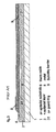
- Fig. 1 shows such an arrangement schematically.
- the more weakly doped semiconductor layer of the first doping which is necessary for producing the Schottky contact (9) is applied to a highly doped substrate (1) also with a first doping.
- the object of the invention is to increase the reverse current strength of Schottky barrier diodes of the general type while at the same time minimising the forward voltage drop by means of a suitable construction. It is irrelevant whether they are Schottky diodes on an n-conducting or p-conducting epitaxial layer. Furthermore, the embodiment according to the invention is applicable to all semiconductor materials and crystal orientations which are considered for Schottky diodes.
- a significant stabilisation of the high current behaviour with minimisation of the forward voltage drop at the same time is achieved according to the invention in that, in the diffusion region (3) of the second doping type, a more highly doped region of the same conductivity mode (5) is introduced in such a manner that the region of the first conductivity mode (2) which is covered by the barrier metal silicide (9) and the second conductivity mode (3) are connected in a conductive manner.
- the region (3) of the second conductivity mode is diffused in such a manner that it reaches the more highly doped region (1) of the first conductivity mode (1), with at the same time an outward diffusion of the dopand taking place in the direction of the semiconductor surface from the more highly doped substrate layer (1) into the more weakly doped layer (2) of the same conductivity mode.
- the impurity concentration in the region (3) of the second conductivity mode is to be selected such that it is higher than the impurity concentration in the epitaxial layer (2) of the first conductivity mode.
- the invention differs from the standard variant of a highly doped guard ring area (31) of the second conductivity mode in a more weakly doped epitaxial layer (2) of the first conductivity mode.
- the inhibiting junctions are now vertical from the region (3) to the substrate (1), in the presented example without loss of generality a pn+ junction (10) and a laterally aligned pn junction (11) from the region (3) of the second conductivity mode to the epitaxial layer (2) of the first conductivity mode.
- the propagation of the depletion region takes place in the vertical direction primarily into the p-region (3) and in the lateral direction both into the p-region (3) and also into the n epitaxial layer (2), as this is a quasilinear junction because of the doping conditions.
- a p+ enhancement layer (5) is according to the invention implanted in the central, near-surface area of (3).
- a further measure for widening the electrical field in the surface area of the diffused region (3) consists in introducing a linearization ring (4) of the second doping type, which is produced at the same time as the introduction of the region (5) (see Fig. (5 )).
- This introduced region (4) can be connected to the metal layer (8) above it for better potential homogenisation in the guard ring ( Fig. 6 ). In doing so, it is achieved that the surge current strength increases in reverse mode, as an equitinearization of the electrical field takes place along the p-region. This produces a homogenisation of the field in the corners of the guard ring which are particularly at risk of breakdown.
- FIG. 1 A semiconductor arrangement of the conventional type which is reproduced in Fig. 1 shows the cross section through a Schottky barrier diode in which a more weakly doped epitaxial layer (2) of the first conductivity mode has been applied to a highly doped substrate (1) of the same conductivity mode.
- the pn junction of the diffused guard ring region (31) is connected electrically parallel to the Schottky junction (9), with the difference W Epi - x j of the layer thickness W Epi of the more weakly doped layer of the first conductivity mode (2) and the depth x j of the pn junction of the diffused guard ring zone (31) of the second conductivity mode defining the maximum breakdown voltage which can be achieved with the guard ring.
- the metal semiconductor layer (9) which forms the Schottky contact partially overlaps the surface of the guard ring (31).
- the epitaxial layer thickness of the first conductivity mode W Epi which is necessary here is produced from the residual layer thickness W Epi - x j under the guard ring which is necessary for the voltage class plus an additional thickness ⁇ X Epi which corresponds to the penetration depth of the guard ring of the respective voltage class.
- the disadvantage of all these embodiments is an insufficient resistance to reverse surge current loads, which usually lead to failures in the area of the guard ring (31) which is covered by the Schottky barrier layer (9). Also disadvantageous is the unavoidable voltage drop in the forward direction I conduct x R ⁇ xepi which occurs across the epitaxial layer ⁇ X epi .
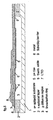
- Fig. 3 shows a detailed illustration of the guard ring area of a conventional arrangement.
- a more weakly doped epitaxial layer (2) of the first conductivity mode is applied to a highly doped substrate (1) of the same conductivity mode, in this case for example a highly doped n-conducting substrate, with the specific resistance and layer thickness depending on the maximum reverse voltage V R to be achieved.
- V R maximum reverse voltage
- the region of the second conductivity mode (3) in this case a p-conducting region, is introduced in such a manner that it penetrates into the highly doped region of the first conductivity mode (1), at the same time a shift of the homojunction (12) takes place from the highly doped region (1) to the more weakly doped region (2) in the direction of the semiconductor surface by autodoping of the more weakly doped layer (2) of the first conductivity mode.
- the region (3) of the second conductivity mode is diffused through the epitaxial layer (2) of the first conductivity mode until it reaches the highly doped region (1) of the first conductivity mode and the highly doped region (1) of the first conductivity mode diffuses toward the epitaxial layer (2) of the first conductivity mode until the near-surface lateral diffusion X lateral is greater than the vertical advance of the diffusion front y vertical .
- a rise in the guard ring doping of the same second conductivity mode is implanted in the near-surface area (5), in the case under consideration here a p+ doped area.
- the p/n+ junction (10) is shifted in the direction of the surface owing to autodoping of the homojunction with respect to the original depth of the junction from the substrate layer (1) of the first conductivity mode to the epitaxial layer (2) of the same conductivity mode.
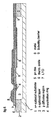
- FIG. 4 The detailed illustration of the embodiment according to the invention of the guard ring area is shown in Fig. 4 .
- An LTO-CVD SiO 2 layer is then applied, in which the window for the deposition of the barrier metal (9) is opened.
- the contact metal is applied and structured in a known manner.
- the metallisation of the rear of the semiconductor arrangement takes place in a conventional manner.
- the linearization ring (4) with the same doping which is at a distance from the region (5) is produced simultaneously with the implantation of the more highly doped region (5) of the second doping, which linearization ring effects a homogenisation of the electrical field in the near-surface area (3) which is produced by the lateral diffusion X lateral .
- Fig. 6 shows an exemplary embodiment in which this linearization ring (4) is connected to the potential of the silicide layer via the contact metal (8) by means of an open contact face.
- Fig. 5 and Fig. 6 result in a further stabilisation of the surge current behaviour.
- Fig. 7 the arrangement of the linearization ring in the corners of the guard ring area is shown, in this case a deactivation of the electrical fields is particularly effective for a breakdown which occurs as late as possible.
- the regions (4) and (5) with an increased concentration of the second conductivity mode are corrected in accordance with the mask in the corner areas in such a manner that a uniform field distribution is achieved even with the lateral diffusion in the corner areas.
Landscapes
- Electrodes Of Semiconductors (AREA)
Applications Claiming Priority (1)
| Application Number | Priority Date | Filing Date | Title |
|---|---|---|---|
| DE102009018971A DE102009018971A1 (de) | 2009-04-25 | 2009-04-25 | Konstruktion einer Schottkydiode mit verbessertem Hochstromverhalten und Verfahren zu deren Herstellung |
Publications (2)
| Publication Number | Publication Date |
|---|---|
| EP2244284A2 true EP2244284A2 (fr) | 2010-10-27 |
| EP2244284A3 EP2244284A3 (fr) | 2011-06-15 |
Family
ID=42355342
Family Applications (1)
| Application Number | Title | Priority Date | Filing Date |
|---|---|---|---|
| EP10160364A Withdrawn EP2244284A3 (fr) | 2009-04-25 | 2010-04-19 | Diode Schottky dotée d'un comportement amélioré au courant élevé et son procédé de fabrication |
Country Status (6)
| Country | Link |
|---|---|
| US (1) | US8525288B2 (fr) |
| EP (1) | EP2244284A3 (fr) |
| JP (1) | JP2010258450A (fr) |
| CN (1) | CN101872791A (fr) |
| DE (1) | DE102009018971A1 (fr) |
| TW (1) | TWI424573B (fr) |
Families Citing this family (3)
| Publication number | Priority date | Publication date | Assignee | Title |
|---|---|---|---|---|
| CN103681318B (zh) * | 2012-09-18 | 2016-06-29 | 桂林斯壮微电子有限责任公司 | 使用硅的选择氧化技术制造结势垒肖特基二极管的方法 |
| JP6202944B2 (ja) | 2013-08-28 | 2017-09-27 | 三菱電機株式会社 | 炭化珪素半導体装置およびその製造方法 |
| EP3268991A1 (fr) * | 2015-06-02 | 2018-01-17 | Diotec Semiconductor AG | Dispositif à semi-conducteur amélioré comportant une diode schottky |
Citations (4)
| Publication number | Priority date | Publication date | Assignee | Title |
|---|---|---|---|---|
| US4206540A (en) | 1978-06-02 | 1980-06-10 | International Rectifier Corporation | Schottky device and method of manufacture using palladium and platinum intermetallic alloys and titanium barrier |
| US5780996A (en) * | 1995-06-23 | 1998-07-14 | Nippondenso Co., Ltd. | Alternating current generator and schottky barrier diode |
| DE19939484A1 (de) | 1998-09-01 | 2000-03-09 | Int Rectifier Corp | Schottky-Diode |
| US6177712B1 (en) | 1996-12-10 | 2001-01-23 | Fuji Electric Co., Ltd. | Schottky barrier diode having a guard ring structure |
Family Cites Families (13)
| Publication number | Priority date | Publication date | Assignee | Title |
|---|---|---|---|---|
| JPS4823334Y1 (fr) * | 1968-11-04 | 1973-07-06 | ||
| JPS60143496A (ja) * | 1983-12-29 | 1985-07-29 | Fujitsu Ltd | 半導体記憶装置 |
| JP2667477B2 (ja) | 1988-12-02 | 1997-10-27 | 株式会社東芝 | ショットキーバリアダイオード |
| US5345101A (en) * | 1993-06-28 | 1994-09-06 | Motorola, Inc. | High voltage semiconductor structure and method |
| DE19740195C2 (de) * | 1997-09-12 | 1999-12-02 | Siemens Ag | Halbleiterbauelement mit Metall-Halbleiterübergang mit niedrigem Sperrstrom |
| DE19853743C2 (de) * | 1998-11-21 | 2000-10-12 | Micronas Intermetall Gmbh | Halbleiter-Bauelement mit wenigstens einer Zenerdiode und wenigstens einer dazu parallel geschalteten Schottky-Diode sowie Verfahren zum Herstellen der Halbleiter-Bauelemente |
| JP4447065B2 (ja) * | 1999-01-11 | 2010-04-07 | 富士電機システムズ株式会社 | 超接合半導体素子の製造方法 |
| US6515345B2 (en) * | 2001-02-21 | 2003-02-04 | Semiconductor Components Industries Llc | Transient voltage suppressor with diode overlaying another diode for conserving space |
| JP4872158B2 (ja) * | 2001-03-05 | 2012-02-08 | 住友電気工業株式会社 | ショットキーダイオード、pn接合ダイオード、pin接合ダイオード、および製造方法 |
| JP3708057B2 (ja) * | 2001-07-17 | 2005-10-19 | 株式会社東芝 | 高耐圧半導体装置 |
| US7321682B2 (en) | 2002-11-12 | 2008-01-22 | Namco Bandai Games, Inc. | Image generation system, image generation method, program, and information storage medium |
| JP4921880B2 (ja) * | 2006-07-28 | 2012-04-25 | 株式会社東芝 | 高耐圧半導体装置 |
| US7875950B2 (en) * | 2007-03-08 | 2011-01-25 | Semiconductor Components Industries, Llc | Schottky diode structure with multi-portioned guard ring and method of manufacture |
-
2009
- 2009-04-25 DE DE102009018971A patent/DE102009018971A1/de not_active Ceased
-
2010
- 2010-04-19 CN CN201010166236A patent/CN101872791A/zh active Pending
- 2010-04-19 US US12/762,844 patent/US8525288B2/en not_active Expired - Fee Related
- 2010-04-19 EP EP10160364A patent/EP2244284A3/fr not_active Withdrawn
- 2010-04-19 JP JP2010095923A patent/JP2010258450A/ja active Pending
- 2010-04-19 TW TW099112249A patent/TWI424573B/zh not_active IP Right Cessation
Patent Citations (4)
| Publication number | Priority date | Publication date | Assignee | Title |
|---|---|---|---|---|
| US4206540A (en) | 1978-06-02 | 1980-06-10 | International Rectifier Corporation | Schottky device and method of manufacture using palladium and platinum intermetallic alloys and titanium barrier |
| US5780996A (en) * | 1995-06-23 | 1998-07-14 | Nippondenso Co., Ltd. | Alternating current generator and schottky barrier diode |
| US6177712B1 (en) | 1996-12-10 | 2001-01-23 | Fuji Electric Co., Ltd. | Schottky barrier diode having a guard ring structure |
| DE19939484A1 (de) | 1998-09-01 | 2000-03-09 | Int Rectifier Corp | Schottky-Diode |
Also Published As
| Publication number | Publication date |
|---|---|
| US20100283115A1 (en) | 2010-11-11 |
| TW201041148A (en) | 2010-11-16 |
| US8525288B2 (en) | 2013-09-03 |
| EP2244284A3 (fr) | 2011-06-15 |
| CN101872791A (zh) | 2010-10-27 |
| DE102009018971A1 (de) | 2010-11-04 |
| JP2010258450A (ja) | 2010-11-11 |
| TWI424573B (zh) | 2014-01-21 |
Similar Documents
| Publication | Publication Date | Title |
|---|---|---|
| US9312346B2 (en) | Semiconductor device with a charge carrier compensation structure and method for the production of a semiconductor device | |
| US9076861B2 (en) | Schottky and MOSFET+Schottky structures, devices, and methods | |
| US8497563B2 (en) | Semiconductor device and method for its manufacture | |
| US9553179B2 (en) | Semiconductor device and insulated gate bipolar transistor with barrier structure | |
| US10256325B2 (en) | Radiation-hardened power semiconductor devices and methods of forming them | |
| US9583578B2 (en) | Semiconductor device including an edge area and method of manufacturing a semiconductor device | |
| US7282386B2 (en) | Schottky device and method of forming | |
| US20110024791A1 (en) | Bipolar semiconductor device and manufacturing method | |
| US20140231909A1 (en) | Super Junction Semiconductor Device Comprising Implanted Zones | |
| US20150380542A1 (en) | Charge Compensation Structure and Manufacturing Therefor | |
| US9859383B2 (en) | Schottky diode with reduced forward voltage | |
| US9006062B2 (en) | Method of manufacturing a semiconductor device including an edge area | |
| US9263599B2 (en) | Semiconductor system and method for manufacturing same | |
| US10164043B2 (en) | Semiconductor diode and method for forming a semiconductor diode | |
| US9865717B2 (en) | Semiconductor device | |
| US11387359B2 (en) | Ppower semiconductor device with anticorrosive edge termination structure | |
| US9368649B2 (en) | Schottky barrier diode and method of manufacturing the same | |
| JPH1168106A (ja) | トランジスタ構成素子とその製造方法 | |
| EP2244284A2 (fr) | Diode Schottky dotée d'un comportement amélioré au courant élevé et son procédé de fabrication | |
| KR20070026690A (ko) | 쇼트키 소자와 형성 방법 | |
| US11056595B2 (en) | Semiconductor device and manufacturing method thereof | |
| US12513921B2 (en) | Semiconductor device including a field stop region | |
| US20220406922A1 (en) | Semiconductor device including protruding region | |
| US20090194843A1 (en) | Integrated circuit arrangement including a protective structure | |
| EP3460856B1 (fr) | Diode à barrière de schottky avec contact schottky amélioré pour hautes tensions |
Legal Events
| Date | Code | Title | Description |
|---|---|---|---|
| PUAI | Public reference made under article 153(3) epc to a published international application that has entered the european phase |
Free format text: ORIGINAL CODE: 0009012 |
|
| AK | Designated contracting states |
Kind code of ref document: A2 Designated state(s): AT BE BG CH CY CZ DE DK EE ES FI FR GB GR HR HU IE IS IT LI LT LU LV MC MK MT NL NO PL PT RO SE SI SK SM TR |
|
| AX | Request for extension of the european patent |
Extension state: AL BA ME RS |
|
| 17P | Request for examination filed |
Effective date: 20101102 |
|
| PUAL | Search report despatched |
Free format text: ORIGINAL CODE: 0009013 |
|
| AK | Designated contracting states |
Kind code of ref document: A3 Designated state(s): AT BE BG CH CY CZ DE DK EE ES FI FR GB GR HR HU IE IS IT LI LT LU LV MC MK MT NL NO PL PT RO SE SI SK SM TR |
|
| AX | Request for extension of the european patent |
Extension state: AL BA ME RS |
|
| 17Q | First examination report despatched |
Effective date: 20140106 |
|
| STAA | Information on the status of an ep patent application or granted ep patent |
Free format text: STATUS: THE APPLICATION IS DEEMED TO BE WITHDRAWN |
|
| 18D | Application deemed to be withdrawn |
Effective date: 20170208 |