EP2244296B1 - Mehrschichtige Bildsensorpixelstruktur zur Übersprechungsreduzierung - Google Patents
Mehrschichtige Bildsensorpixelstruktur zur Übersprechungsreduzierung Download PDFInfo
- Publication number
- EP2244296B1 EP2244296B1 EP10250805.8A EP10250805A EP2244296B1 EP 2244296 B1 EP2244296 B1 EP 2244296B1 EP 10250805 A EP10250805 A EP 10250805A EP 2244296 B1 EP2244296 B1 EP 2244296B1
- Authority
- EP
- European Patent Office
- Prior art keywords
- layer
- type
- image sensor
- barrier layer
- pixel
- Prior art date
- Legal status (The legal status is an assumption and is not a legal conclusion. Google has not performed a legal analysis and makes no representation as to the accuracy of the status listed.)
- Active
Links
Images





Classifications
-
- H—ELECTRICITY
- H10—SEMICONDUCTOR DEVICES; ELECTRIC SOLID-STATE DEVICES NOT OTHERWISE PROVIDED FOR
- H10F—INORGANIC SEMICONDUCTOR DEVICES SENSITIVE TO INFRARED RADIATION, LIGHT, ELECTROMAGNETIC RADIATION OF SHORTER WAVELENGTH OR CORPUSCULAR RADIATION
- H10F39/00—Integrated devices, or assemblies of multiple devices, comprising at least one element covered by group H10F30/00, e.g. radiation detectors comprising photodiode arrays
- H10F39/80—Constructional details of image sensors
- H10F39/807—Pixel isolation structures
-
- H—ELECTRICITY
- H10—SEMICONDUCTOR DEVICES; ELECTRIC SOLID-STATE DEVICES NOT OTHERWISE PROVIDED FOR
- H10F—INORGANIC SEMICONDUCTOR DEVICES SENSITIVE TO INFRARED RADIATION, LIGHT, ELECTROMAGNETIC RADIATION OF SHORTER WAVELENGTH OR CORPUSCULAR RADIATION
- H10F39/00—Integrated devices, or assemblies of multiple devices, comprising at least one element covered by group H10F30/00, e.g. radiation detectors comprising photodiode arrays
- H10F39/80—Constructional details of image sensors
Definitions
- Image sensors have become ubiquitous. They are widely used in digital still cameras, cellular phones, security cameras, as well as in, medical, automobile, and other applications.
- the technology used to manufacture image sensors, and in particular, complementary metal-oxide-semiconductor (“CMOS”) image sensors (“CIS”) has continued to advance at great pace. For example, the demands of higher resolution and lower power consumption have encouraged the further miniaturization and integration of these image sensors.
- CMOS complementary metal-oxide-semiconductor
- CIS complementary metal-oxide-semiconductor
- FIG. 1 illustrates a conventional front side illuminated CIS pixel 100.
- the front side of CIS pixel 100 is the side of a P+ substrate 105 upon which pixel circuitry 130 is disposed and over a which metal stack 110 for redistributing signals is formed.
- the metal layers e.g., metal layer M1 and M2 are patterned in such a manner as to create an optical passage through which light (indicated by dashed arrows) incident on the front side of CIS pixel 100 can reach a photosensitive or photodiode (“PD") region 115.
- the front side of CIS pixel 100 further includes a color filter layer 120 disposed under a microlens 125. Microlens 125 aids in focusing the light onto PD region 115.
- CIS pixel 100 includes pixel circuitry 130 (indicated by a dashed rectangle) disposed adjacent to PD region 115 within a P doped welL Pixel circuitry 130 provides a variety of functionality for regular operation of CIS pixel 100.
- pixel circuitry 130 may include circuitry to commence acquisition of an image charge within PD region 115, to reset the image charge accumulated within PD region 115 to ready CIS pixel 100 for the next image, or to transfer out the image data acquired by CIS pixel 100.
- FIG. 2 illustrates details of a portion of two neighboring CIS pixels 100 formed within a P- epitaxial (“epi") layer 140 disposed over P+ substrate 105 and separated by shallow trench isolation regions (STI).
- epi P- epitaxial
- STI shallow trench isolation regions
- a photo-generated charge carrier When a photo-generated charge carrier is formed deeper within the CIS pixel (e.g., a second charge carrier 155), it initially experiences a weaker upward repulsive force due to the presence of a dopant gradient at the junction between P- epi layer 140 and P+ substrate 105.
- Crosstalk is a serious problem in image sensors.
- Electrical crosstalk results when charge carriers generated in one pixel of an image sensor are collected by a neighboring pixel of the image sensor.
- Optical crosstalk can be caused by the diffraction and/or scattering of light off of metal lines and at interfaces between the dielectric layers within metal stack 110.
- Spectral crosstalk results from the finite (nonzero) transmittance of color filter 120 to wavelengths outside its target pass band, such as the finite transmittance of green and blue wavelengths through a red filter.
- One form of electrical crosstalk is lateral drift of photo-generated charge carriers created deep in the semiconductor epitaxial layers (e.g., second charge carrier 155). As these photo-generated charge carriers rise, they can drift laterally and end up collected in the PD region of a neighboring pixel. Blooming is another form of electrical crosstalk characterized by the lateral diffusion of charge carriers when a PD region becomes full or saturated with charge carriers. Blooming is most commonly experienced in high luminous environments. Photo carriers that are generated near a saturated PD region 115 will not be collected and therefore remain free to diffuse laterally into a neighboring pixel. Blooming results in the blurring of edges in still images and streaking in moving images. Both forms of electrical crosstalk are due to charge carriers generated in one pixel being collected by a neighboring pixel.
- WO 2007/024819 discloses a solid-state imager device having a patterned buried doped region in the substate, preferably an n+ doped region, that collects excess electrons and thus reduces cross-talk, minimizes blooming of excess electrons, and reduces dark current in a solid-state imager device, and a corresponding fabrication method.
- the present invention provides an image sensor pixel as set out in claim 1 and a method as set out in claim 11.
- electrical crosstalk between image sensor pixels is reduced relative to traditional image sensor pixels by disposing a collector layer below the photodiode regions which acts to prevent carriers formed deep within the photodiode regions from being collected in neighboring photodiode regions. Under proper bias conditions a field is established by which photo-generated carriers are swept away from locations deep within the photodiode regions and collected by the collector layer below the photodiode regions in order to prevent their collection by adjacent photodiodes.
- electrical crosstalk between image sensor pixels is reduced relative to traditional image sensor pixels by disposing a barrier layer at least partially covering a collector layer, the barrier layer acting to prevent carriers formed deep within the photodiode regions from being collected in neighboring photodiode regions.
- a field is established by which photo-generated carriers are swept away from locations deep within the photodiode regions and collected by the collector layer below the photodiode regions in order to prevent their collection by adjacent photodiodes.
- a field between the barrier layer and the photodiode region that provides for increased collection within the photodiode regions of carriers generated moderately deep within photodiode regions.
- FIG. 1 is a cross sectional view of a conventional front side illuminated CMOS image sensor pixel.
- FIG. 2 is a cross sectional view of two neighboring CMOS image sensor pixels illustrating a mechanism for electrical crosstalk.
- FIG. 3 is a cross sectional view of two neighboring CMOS image sensor pixels having a structure that reduces electrical crosstalk, in accordance with an example useful for understanding the invention.
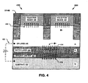
- FIG. 4 is a cross sectional view of two neighboring CMOS image sensor pixels having a structure that reduces electrical crosstalk, in accordance with an example useful for understanding the invention.
- FIG. 5 is a cross sectional view of two neighboring image sensor pixels having a structure that reduces electrical crosstalk, in accordance with an example useful for understanding the invention.
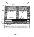
- FIG. 6 is a cross sectional view of two neighboring image sensor pixels having a structure that reduces electrical crosstalk, in accordance with an embodiment.
- FIG. 7 is a cross sectional view of two neighboring image sensor pixels having a structure that reduces electrical crosstalk, in accordance with an embodiment.
- FIG.8 is a functional block diagram illustrating a sensor, in accordance with an embodiment.
- FIG. 9 is a circuit diagram illustrating sample pixel circuitry of two image sensor pixels within an image sensor array, in accordance with an embodiment
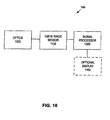
- FIG. 10 is a block diagram illustrating an imaging system with reduced electrical crosstalk, in accordance with an embodiment.
- Embodiments of a pixel, an image sensor, an imaging system, and methods of fabrication of a pixel, image sensor, and imaging system having improved electrical crosstalk characteristics are described herein.
- numerous specific details are set forth to provide a thorough understanding of the embodiments.
- One skilled in the relevant art will recognize, however, that the techniques described herein can be practiced without one or more of the specific details, or with other methods, components, materials, etc.
- well-known structures, materials, or operations are not shown or described in detail to avoid obscuring certain aspects.
- image sensor pixels reference numbers 300, 400, 500, 600, and 700 in the figures
- each pixel may include pixel circuitry (e.g., as shown in FIG. 9 ) coupled to its collection region for performing a variety of functions, such as commencing image acquisition, resetting accumulated image charge, transferring out acquired image data, or otherwise.
- FIG. 3 is a cross sectional view of two neighboring CIS pixels 300A and 300B (collectively pixels 300) having a multilayer structure that reduces electrical crosstalk, in accordance with an example useful for understanding the invention.
- the illustrated example of pixels 300 include a substrate 305, a gradient junction 307, an epitaxial (“epi") layer 315, collection regions 320, and a biasing circuit 325.
- Collection regions 320 of pixels 300A and 300B are isolated from each other by shallow trench isolations ("STI") 360 and dopant wells 330.
- a pinning layer 335 overlays collection regions 320 to passivate their surfaces.
- substrate 305 is a silicon substrate highly doped with N type dopants (e.g., Arsenic; Phosphorous) while epi layer 315 is a silicon layer lightly doped with P type dopants (e.g., Boron).
- Collection regions 320 represent photosensitive regions (e.g., photodiode), which are doped with the same conductivity type as substrate 305.
- Dopant wells 330 are P wells for isolating adjacent collection regions 320 and preventing a direct interface between STI 360 and collection regions 320.
- the conductivity types of all the elements can be swapped such that substrate 305 is P+ doped, epi layer 315 is N- doped, collection regions 320 are P+ doped, and dopant wells 330 are N doped.
- N type substrates may include silicon wafers doped with high concentrations of Arsenic or Phosphorous (also referred to as N+ substrates).
- Traditional CIS pixels typically use P type epitaxial layers (e.g., P- epi layer 315) disposed on P+ substrates
- P type epi layer 315 may be fabricated by growing the P type epi layer on the N+ substrate.
- Electric field 340 (indicated by arrows) formed at the interface between P- epi layer 315 and N+ substrate 305 acts as a barrier to photo generated charge carriers (e.g., photo electrons) that are formed in N+ substrate 305.
- This barrier lowers the probability that a charge carrier formed deep in the CIS pixel structure can diffuse to an adjacent collection region 320. Similarly, this structure reduces blooming. If collection region 320 is full, uncollected electrons are drawn into N+ substrate 305 by electric field 340, rather than diffusing down around dopant wells 330 and into a neighboring collection region 320.
- the junction between P- epi layer 315 and N+ substrate 305 is not infinitely abrupt.
- the N+ substrate is typically heavily doped with As or P.
- N type dopants may diffuse into P- epi layer 315.
- thermal processing associated with CIS fabrication increases the N type dopant diffusion into epi layer 315.
- the junction between substrate 305 and epi layer 315 is graded (illustrated as gradient junction 307). Electric field 340, and therefore the field barrier generated to reduce crosstalk and blooming, is dependent on the diffusion gradient profile. The final thickness of epi layer 315 after diffusion is thus dependent on the diffusion gradient profile. Because collection regions 320 are disposed within epi layer 315, the light collection efficiency and the degree of lateral charge carrier diffusion and blooming will vary with the CIS process thermal budget and the epitaxial layer growth process.
- photo-generated charge carriers that are created shallow within epi layer 315 are collected by the electric field generated by the depletion region at the P-N junction between collection region 320 and epi layer 315.
- photo-generated charge carriers that are created deep within epi layer 315 have a statistically increased chance of being drawn into substrate 305 by electric field 340 where they recombine without contributing to crosstalk.
- photo-generated charge carriers that are created even deeper within substrate 305 are inhibited from diffusing up into a neighboring collection region 320 by the potential barrier created by field 340.
- substrate 305 can be positively biased relative to epi layer 315 and collection regions 320 by biasing circuit 325.
- biasing circuit 325 would be used to negatively bias substrate 305 relative to epi layer 315.
- FIG. 4 is a cross sectional view of two neighboring CIS pixels 400A and 400B (collectively pixels 400) having a multilayer structure that reduces electrical crosstalk, in accordance with an example useful for understanding the invention.
- Pixels 400 are similar to pixels 300 with the following exceptions.
- Pixels 400 include an additional buffer layer 410 having the same conductivity type doping as a substrate 405, but in a lesser concentration. Since the N type dopant concentration interface is not infinitely abrupt, a gradient junction 407 represents a graded dopant profile from N+ substrate 405 to a N- buffer layer 410.
- pixels 400 may also include biasing circuit 425 to bias substrate 405 relative to collection regions 420 and an epi layer 415 (e.g., positive for N type substrate and collection regions or negatively for a P type substrate and collection regions).
- the depletion region formed at the interface of N- buffer layer 410 and P- epi layer 415 generates an electric field 414, which draws deep photo-electrons into buffer layer 410 where they can recombine.
- a dopant gradient field 416 is generated at gradient junction 407, which also pulls photo-electrons generated in buffer layer 410 into substrate 405 or impedes the diffusion of photo-electrons generated in substrate 405 from migrating into buffer layer 410 and from there into epi layer 415.
- buffer layer 410 is an epitaxial layer grown over substrate 405 and serves a dual purpose. First, buffer layer 410 traps deep or excess photo-electrons resulting in a reduction in crosstalk and blooming. Second, buffer layer 410 serves as an N type diffusion buffer, preventing the high concentration N type dopants of substrate 405 from diffusing into the P type epi layer 415 during epitaxial growth cycles and the other high temperature CIS processes. The dopant concentration in buffer layer 410 is significantly lower than substrate 405, resulting in significantly less N type dopant diffusion into the P type epi layer 415. As such, buffer layer 410 can increase the thermal budget of pixels 400 during fabrication. Buffer layer 410 adds process margin to device fabricated on N+ substrates, which eases process development and process transfers. In addition, this multilayer structure is less dependent on a particular wafer vendor's growth conditions, allowing wider sources of starting material.
- the lower thickness limit to buffer layer 410 is determined by the amount of dopant diffusion expected from substrate 405.
- the upper limit to the thickness of buffer layer 410 is not limited by the fabrication process. Photo-electrons present in buffer layer 410 will more easily diffuse to substrate 405 than cross the P-N junction barrier of field 414. Therefore a wide margin can be used in choosing the thickness of buffer layer 410.
- buffer layer 410 may range from approximately 0.3 ⁇ m to 10 ⁇ m.
- additional layers, in conjuction with optional applied bias from biasing circuit 425, to create additional barriers to diffusion of photo-generated carriers, may be further advantageous in reducing electrical crosstalk between image sensor pixels. The use of such additional layers is described herein in the following embodiments.
- FIG. 5 is a cross sectional view of two neighboring image sensor pixels 500A and 500B (collectively pixels 500) having a multilayer structure that reduces electrical crosstalk, in accordance with an example useful for understanding the invention.
- Pixels 500 are similar to pixels 400 with the following exceptions.
- Pixels 500 include a barrier layer 512 disposed between an epi layer 515 and buffer layer 510.
- Barrier layer 512 has the same conductivity type as epi layer 515 (e.g., P type), but with a greater dopant concentration than epi layer 515.
- pixels 500 include barrier layer 512, but lack buffer layer 510. Fabrication of such an example may have less complexity but may also have reduced performance.
- Barrier layer 512 serves at least two purposes. On the photodiode side, barrier layer 512 creates an electric field 513 that drives photo-electrons present in epi layer 515 up towards collection regions 520. On the substrate side, the depletion region formed at the interface of barrier layer 512 and buffer layer 510 creates an electric field 514 which draws deep photo-generated carriers into the buffer layer where they recombine. Electric field 514 is also a potential barrier that photo-generated carriers in buffer layer 510 must overcome to diffuse into epi layer 515. Accordingly, barrier layer 512 impedes deep photo-electrons from migrating into neighboring collection region 520 while promoting the collection of shallow photo-electrons by driving them upwards toward collection region 520 and mitigating lateral drift.
- pixels 500 may also include a biasing circuit 525 to bias substrate 505 relative to collection regions 520 and epi layer 515 (e.g., positive for N type substrate and N type collection regions or negatively for a P type substrate and P type collection regions).
- FIG. 6 is a cross sectional view of two neighboring image sensor pixels 600A and 600B (collectively pixels 600) having a multilayer structure that reduces electrical crosstalk, in accordance with an embodiment.
- the illustrated example of pixels 600 includes a substrate 605,an epitaxial ("epi") layer 607, a collector layer 610, a barrier layer 612, an epi layer 615, collection regions 620, and a biasing circuit 625.
- the collection regions 620 of each pixel 600 are isolated from each other with STI 660 and dopant wells 630.
- a pinning layer 635 overlays collection regions 620 to passivate their surfaces.
- substrate 605 is a silicon substrate highly doped with P type dopants (e.g., Boron) while epi layers 607 and 615 are silicon layers lightly doped with P type dopants (e.g., Boron).
- Collector layer 610 is doped with N type dopants.
- Barrier layer 612 is doped with P type dopants, but with a greater dopant concentration than epi layer 615.
- Collection regions 620 represent photosensitive regions (e.g., photodiodes), which are doped with the N-type dopants.
- Dopant wells 630 are P wells for isolating adjacent collection regions 620 and preventing a direct interface between STI 660 and collection regions 620.
- dopant wells 630 optionally extend down to reach barrier layer 612 (illustrated in FIG. 6 ). By electrically coupling dopant wells 630 to barrier layer 612, excess charges that are formed or migrate into dopant wells 630 are electrostatically carried away from collection regions 620 and drawn down into collector layer 610.
- any applied bias voltage at biasing circuit 625 would have a polarity opposite that illustrated in FIG. 6 .
- Barrier layer 612 serves at least two purposes. On the photodiode side, barrier layer 612 creates an electric field 613 that drives photo-electrons present in epi layer 615 up towards collection regions 620. On the substrate side, the depletion region formed at the interface of barrier layer 612 and buried collector layer 610 creates an electric field 614 that draws deep photo-generated carriers into the buried collector layer where they recombine. Electric field 614 is also a potential barrier that photo-generated carriers in collector layer 610 must overcome to diffuse into epi layer 615. Accordingly, barrier layer 612 impedes deep photo-electrons from migrating into a neighboring collection region 620 while promoting the collection of shallow photo-electrons by driving them towards collection region 620 and mitigating their lateral migration.
- Barrier layer 612 may have a thickness of approximately 0.3 ⁇ m to 10 ⁇ m and a doping concentration of approximately 2x10 16 atoms/cm 3 to 2x10 18 atoms/cm 3 .
- Collector layer 610 may have a thickness of approximately 0.3 ⁇ m to 10 ⁇ m and a dopant concentration of approximately 1x10 16 atoms/cm 3 to 1x10 18 atoms/cm 3 . In one embodiment, the doping concentration of collector layer 610 is less than the doping concentration of barrier layer 612.
- pixels 600 may also include a biasing circuit 625 to bias collector layer 610 relative to epi layer 615 (e.g., positive for N type collection regions or negatively for P type collection regions).
- photo-generated charge carriers that are created shallow within epi layer 615 are collected by electric field 618 generated by the depletion region at a P-N junction formed between collection region 620 and epi layer 615.
- photo-generated charge carriers that are created deep within epi layer 615 may either be driven up towards collection regions 620 by electric field 613 or be drawn into collector layer 610 by electric field 614 where they recombine without contributing to crosstalk.
- any additional carriers may overcome electric field 613 and be drawn by electric field 614 into collector layer 610 without contributing to blooming.
- collector layer 610 can be positively biased relative to epi layer 615 and collection regions 620 by biasing circuit 625.
- the presence of the biasing operates to further impede photo-electrons from crossing the potential barrier of field 614.
- Epi layers 607 and 615, and substrate 605 may typically be electrically grounded but depending on the application other structures may be grounded as well. It should be appreciated that in an embodiment where collector layer 610 is P+ doped and epi layer 615 is an N- epi layer, the biasing circuit 625 would negatively bias substrate 610 relative to epi layer 615.
- FIG. 7 is a cross sectional view of two neighboring image sensor pixels 700A and 700B (collectively pixels 700) having a multilayer structure that further reduces electrical crosstalk, in accordance with an embodiment. Pixels 700 are similar to pixels 600 with the following exceptions.
- Collector layer 710 is formed by ion implantation of selected regions of epi layer 707, resulting in the creation of electrical pass-through 702 between barrier layer 712 and epi layer 707 at selected locations.
- Electrical pass-through 702 is an area of epi layer 707 that is not selected to become collector 710 by ion implantation. Electrical pass-through 702 allows for more efficient draining of electrical carriers from epi layer 707 into barrier layer 712.
- barrier layer 712 is doped P type
- photon generated holes may be improperly drained from barrier layer 712 without the presence of electrical pass-through 702.
- Electrical pass-through 702 may be maintained along barrier layer 712 in a specific pattern (e.g. under pixels having one or more specific color filters) or they could be placed less frequently and/or randomly within the array.
- Other design parameters for electrical pass-through 702 such as density and size depend, for example, on the barrier layer resistance, the number of neighboring pixels within a pixel array, and the size of each collection region 720.
- FIG. 8 is a functional block diagram illustrating a CIS 800, in accordance with an embodiment.
- the illustrated embodiment of CIS 800 includes pixel array 805 having improved electrical crosstalk characteristics, readout circuitry 810, function logic 815, and control circuitry 820.
- Pixel array 805 is a two-dimensional ("2D") array of image sensor pixels (e.g., pixels P1, P2 ..., Pn). In one embodiment, each pixel represents any of pixels 300, 400, 500, 600 or 700, illustrated in FIGS. 3-7 . In one embodiment, each pixel is a CIS pixel. In one embodiment, pixel array 805 includes a color filter array including a color pattern (e.g., Bayer pattern or mosaic) of red, green, and blue filters.
- a color pattern e.g., Bayer pattern or mosaic
- each pixel is arranged into a row (e.g., rows R1 to Ry) and a column (e.g., column C1 to Cx) to acquire image data of a person, place, or object, which can then be used to render a 2D image of the person, place, or object.
- a row e.g., rows R1 to Ry
- a column e.g., column C1 to Cx
- Readout circuitry 810 may include amplification circuitry, analog-to-digital ("ADC") conversion circuitry, or otherwise.
- Function logic 815 may simply store the image data or even manipulate the image data by applying post image effects (e.g., crop, rotate, remove red eye, adjust brightness, adjust contrast, or otherwise).
- readout circuitry 810 may readout a row of image data at a time along readout column lines (illustrated) or may readout the image data using a variety of other techniques (not illustrated), such as a column/row readout, a serial readout, or a full parallel readout of all pixels simultaneously.
- Control circuitry 820 is connected with pixel array 805 to control operational characteristic of pixel array 805.
- control circuitry 820 may generate a shutter signal for controlling image acquisition.
- the shutter signal is a global shutter signal for simultaneously enabling all pixels within pixel array 805 to simultaneously capture their respective image data during a single acquisition window.
- the shutter signal is a rolling shutter signal whereby each row, column, or group of pixels is sequentially enabled during consecutive acquisition windows.
- FIG. 9 is a circuit diagram illustrating pixel circuitry 900 of two four-transistor ("4T") pixels within a pixel array, in accordance with an embodiment.
- Pixel circuitry 900 is one possible pixel circuitry architecture for implementing each pixel within pixel array 805 of FIG. 8 .
- the embodiments described herein are not limited to 4T pixel architectures; rather, one of ordinary skill in the art having the benefit of the instant disclosure will understand that the present teachings are also applicable to 3T designs, 5T designs, and various other pixel architectures.
- each pixel circuitry 900 includes a photodiode PD, a transfer transistor T1, a reset transistor T2, a source-follower ("SF") transistor T3, and a select transistor T4.
- transfer transistor T1 receives a transfer signal TX, which transfers the charge accumulated in photodiode PD to a floating diffusion node FD.
- floating diffusion node FD may be coupled to a storage capacitor for temporarily storing image charges.
- Reset transistor T2 is coupled between a power rail VDD and the floating diffusion node FD to reset the pixel (e.g., discharge or charge the FD and the PD to a preset voltage) under control of a reset signal RST.
- the floating diffusion node FD is coupled to control the gate of SF transistor T3.
- SF transistor T3 is coupled between the power rail VDD and select transistor T4.
- SF transistor T3 operates as a source-follower providing a high impedance connection to the floating diffusion FD.
- select transistor T4 selectively couples the output of pixel circuitry 900 to the readout column line under control of a select signal SEL.
- the TX signal, the RST signal, and the SEL signal are generated by control circuitry 820.
- the global shutter signal is coupled to the gate of each transfer transistor T1 in the entire pixel array 805 to simultaneously commence charge transfer from each pixel's photodiode PD.
- rolling shutter signals may be applied to groups of transfer transistors T1.
- FIG. 10 illustrates an imaging system 1000 that utilizes a CMOS image sensor 1100 having image sensor pixel structures providing reduced electrical crosstalk, according to any of the embodiments disclosed herein.
- Image system 1000 further includes imaging optics 1200 for directing light from an object to be imaged onto CMOS image sensor 1100, and may also include a signal processor 1300 for producing processed image data for display on optional display 1400.
- the image sensor pixel may comprise a front side illuminated complementary metal-oxide-semiconductor ("CMOS") image sensor.
- CMOS complementary metal-oxide-semiconductor
- the light collection region of the image sensor pixel may comprise a photo-diode, and the image sensor pixel may also comprise: a metal stack including metal layers for routing signals over the front side of the CMOS image sensor separated by dielectric layers; and a microlens disposed on the metal stack.
Landscapes
- Solid State Image Pick-Up Elements (AREA)
- Light Receiving Elements (AREA)
Claims (18)
- Komplementär-Metalloxid-Halbleiter- ("CMOS"-)Bildsensorpixel (600, 700), umfassend:ein Substrat (605, 705), das so dotiert ist, dass es einen ersten Leitfähigkeitstyp aufweist;eine erste Epitaxialschicht (607, 707), die über dem Substrat (605, 705) angeordnet und so dotiert ist, dass sie den ersten Leitfähigkeitstyp aufweist;eine Sammlerschicht (610, 710), die beliebig über zumindest einem Abschnitt der ersten Epitaxialschicht (607, 707) angeordnet und so dotiert ist, dass sie einen zweiten Leitfähigkeitstyp aufweist;eine zweite Epitaxialschicht (615, 715), die über der Sammlerschicht (610, 710) angeordnet und so dotiert ist, dass sie den ersten Leitfähigkeitstyp aufweist;eine Lichtsammelregion (620, 720) zum Sammeln von Licht-generierten Ladungsträgern, die in der zweiten Epitaxialschicht (615, 715) angeordnet sind, wobei die Lichtsammelregion (620, 720) so dotiert ist, dass sie den zweiten Leitfähigkeitstyp aufweist; und dadurch gekennzeichnet, dasseine Barriereschicht (612, 712) zwischen der zweiten Epitaxialschicht (615, 715) und der Sammlerschicht (610, 710) angeordnet ist, wobei die Barriereschicht (612, 712) so dotiert ist, dass sie den ersten Leitfähigkeitstyp aufweist, aber mit einer größeren Dotierungskonzentration als die zweite Epitaxialschicht (615, 715).
- Bildsensorpixel (600, 700) nach Anspruch 1, worin die Sammelschicht (610, 710) einen elektrischen Durchgang (701) in der Sammelschicht (610, 710) umfasst, damit die Barriereschicht (612, 712) mit der ersten Epitaxialschicht (607, 707) elektrisch verbunden werden kann.
- Bildsensorpixel (600, 700) nach Anspruch 1, worin die Sammelschicht (610, 710) eine Dotierungskonzentration von ungefähr 1016 Atomen/cm3 bis 1017 Atomen/cm3 aufweist.
- Bildsensorpixel (600, 700) nach Anspruch 1, worin die Sammelschicht (610, 710) ungefähr 0,3 µm b is 10 µm dick ist.
- Bildsensorpixel (600, 700) nach Anspruch 1, worin die Barriereschicht (612, 712) eine Dotierungskonzentration von ungefähr 1017 Atomen/cm3 bis 1018 Atomen/cm3 aufweist.
- Bildsensorpixel (600, 700) nach Anspruch 1, worin die Barriereschicht (612, 712) eine Dicke von ungefähr 0,3 µm bis 1,0 µm aufweist.
- Bildsensorpixel (600, 700) nach Anspruch 1, worin der erste Leitfähigkeitstyp P-Typ-Dotierelemente umfasst und der zweite Leitfähigkeitstyp N-Typ-Dotierelemente umfasst.
- Bildsensorpixel (600, 700) nach Anspruch 1, worin der erste Leitfähigkeitstyp N-Typ-Dotierelemente umfasst und der zweite Leitfähigkeitstyp P-Typ-Dotierelemente umfasst.
- Bildsensorpixel (600, 700) nach Anspruch 1, worin die Barriereschicht (612, 712) ein elektrisches Feld erzeugt, das in der zweiten Epitaxialschicht (615, 715) erzeugte Ladungsträger hin zur Lichtsammelregion (629, 720) drückt, wobei gleichzeitig verhindert wird, dass in der Sammlerschicht (619, 710) oder im Substrat erzeugte Ladungsträger, in den Lichtsammelbereich (629, 720) zu dringen.
- Bildsensorpixel (600, 700) nach Anspruch 1, ferner umfassend einen Vorspannungskreis (625, 725), der angeschlossen ist, um die Sammlerschicht (619, 710) relativ zur Barriereschicht vorzuspannen.
- Verfahren zum Antreiben eines Komplementär-Metalloxid-Halbleiter- (CMOS"-)Bildsensors (800) nach Anspruch 1, worin das Verfahren Folgendes umfasst:Sammeln von Ladungsträgern in Sammelregionen (620, 720), die in einer zweiten P-Typ-Epitaxialschicht (615, 715) angeordnet sind, als Antwort auf den CMOS-Bildsensor (800);Erzeugen eines ersten Felds an einer Verbindung zwischen einer N-Typ-Sammlerschicht (610, 710) und einer P-Typ-Barriereschicht (613, 712), um überschüssige in der P-Typ-Barriereschicht (612, 712) erzeugte Ladungsträger von dem Sammelregionen weg und in die N-Typ-Sammlerschicht (610, 710) anzuziehen, worin die N-Typ-Sammlerschicht (610, 710) und die P-Typ-Barriereschicht (612, 712) zwischen einer Substratschicht (605, 705) und der zweiten Expitaxialschicht (615, 715) angeordnet sind; undErzeugen eines zweiten Felds an einer Verbindung zwischen der P-Typ-Barriereschicht (612, 712) und der zweiten Expitaxialschicht (615, 715), um in der zweiten P-Typ-Epitaxialschicht (615, 715) erzeugte Photoelektronen hin zu den Sammelregionen (620, 720) anzuziehen, worin eine erste P-Typ-Epitaxialschicht (607, 707) zwischen der Substratschicht (605, 705) und der zweiten P-Typ-Epitaxialschicht angeordnet ist.
- Verfahren nach Anspruch 11, worin der CMOS-Bildsensor (800) die erste P-Typ-Epitaxialschicht (607, 707) umfasst, die zwischen der Substratschicht (605, 705) und der Sammlerschicht (610, 710) angeordnet ist, wobei das Verfahren Folgendes umfasst:elektrisches Verbinden der ersten P-Typ-Epitaxialschicht (607-707) mit der P-Typ-Barriereschicht (612, 712) über elektrische Durchgänge (702), die beliebig auf der N-Typ-Sammlerschicht (610, 710) angeordnet sind.
- Verfahren nach Anspruch 11, worin die P-Typ-Barriereschicht (612, 712) elektrisch mit P-Vertiefungen verbunden ist, die benachbarte Sammelregionen (620, 720) trennen, wobei das Verfahren ferner Folgendes umfasst:Elektrostatisches Anziehen überschüssiger Ladungsträger in den P-Vertiefungen hinunter durch die Barriereschicht (612, 712) hin zur Sammlerschicht (610, 710).
- Verfahren nach Anspruch 11, worin die P-Typ-Barriereschicht (612, 712) eine höhere Konzentration von P-Typ-Dopierelementen aufweist als die zweite P-Typ-Epitaxialschicht (615, 715), worin das zweite Feld einen P-Typ-Dopierelement-Konzentrationsgradienten aufweist und worin das erste Feld ein elektrostatisches Feld aufgrund einer Verarmungsregion aufweist.
- Verfahren nach Anspruch 11, ferner umfassend das positive Vorspannen der N-Typ-Sammlerschicht (610, 710) relativ zur P-Typ-Barriereschicht (612, 712).
- Abbildungssystem, umfassend:ein Ausleseschaltsystem (810); undeine Komplementär-Metalloxid-Halbleiter- (CMOS"-)Matrix (805) von Abbildungspixeln (600, 700) nach einem der Ansprüche 1 bis 10, wobei jedes Pixel (600, 700) ferner Folgendes umfasst:Dopiervertiefungen zum Isolieren der Lichtsammelregion (620, 720) von der benachbarten Lichtsammelregion (620, 720) von anderen Abbildungspixeln, worin die Dopiervertiefungen den ersten Leitfähigkeitstyp aufweisen;worindas Ausleseschaltsystem (810) an die CMOS-Matrix (805) gekoppelt ist, um Bilddaten von jedem der Abbildungspixel (600, 700) auszulesen.
- Abbildungssystem nach Anspruch 16, worin die Dopiervertiefungen sich durch die zweite Epitaxialschicht (616, 715) erstrecken, um einen elektrischen Kontakt mit der Barriereschicht (612, 712) herzustellen.
- Abbildungssystem nach Anspruch 17, ferner umfassend einen Vorspannungskreis (625, 725), der verbunden ist, um die Sammlerschicht (610, 710) relativ zur Barriereschicht (612, 712) und die Dopiervertiefungen vorzuspannen.
Applications Claiming Priority (1)
| Application Number | Priority Date | Filing Date | Title |
|---|---|---|---|
| US12/430,006 US7875918B2 (en) | 2009-04-24 | 2009-04-24 | Multilayer image sensor pixel structure for reducing crosstalk |
Publications (3)
| Publication Number | Publication Date |
|---|---|
| EP2244296A2 EP2244296A2 (de) | 2010-10-27 |
| EP2244296A3 EP2244296A3 (de) | 2012-06-13 |
| EP2244296B1 true EP2244296B1 (de) | 2014-01-08 |
Family
ID=42269585
Family Applications (1)
| Application Number | Title | Priority Date | Filing Date |
|---|---|---|---|
| EP10250805.8A Active EP2244296B1 (de) | 2009-04-24 | 2010-04-21 | Mehrschichtige Bildsensorpixelstruktur zur Übersprechungsreduzierung |
Country Status (4)
| Country | Link |
|---|---|
| US (2) | US7875918B2 (de) |
| EP (1) | EP2244296B1 (de) |
| CN (1) | CN101872775B (de) |
| TW (1) | TWI416717B (de) |
Cited By (1)
| Publication number | Priority date | Publication date | Assignee | Title |
|---|---|---|---|---|
| TWI692861B (zh) * | 2019-03-14 | 2020-05-01 | 晶相光電股份有限公司 | 影像感測器及其製造方法 |
Families Citing this family (49)
| Publication number | Priority date | Publication date | Assignee | Title |
|---|---|---|---|---|
| KR100870821B1 (ko) * | 2007-06-29 | 2008-11-27 | 매그나칩 반도체 유한회사 | 후면 조사 이미지 센서 |
| JP2011108759A (ja) * | 2009-11-13 | 2011-06-02 | Canon Inc | 固体撮像装置 |
| US20110198689A1 (en) * | 2010-02-17 | 2011-08-18 | Suku Kim | Semiconductor devices containing trench mosfets with superjunctions |
| JP5697371B2 (ja) * | 2010-07-07 | 2015-04-08 | キヤノン株式会社 | 固体撮像装置および撮像システム |
| JP5885401B2 (ja) | 2010-07-07 | 2016-03-15 | キヤノン株式会社 | 固体撮像装置および撮像システム |
| JP5751766B2 (ja) | 2010-07-07 | 2015-07-22 | キヤノン株式会社 | 固体撮像装置および撮像システム |
| JP5656484B2 (ja) | 2010-07-07 | 2015-01-21 | キヤノン株式会社 | 固体撮像装置および撮像システム |
| JP5643555B2 (ja) | 2010-07-07 | 2014-12-17 | キヤノン株式会社 | 固体撮像装置及び撮像システム |
| JP5645513B2 (ja) | 2010-07-07 | 2014-12-24 | キヤノン株式会社 | 固体撮像装置及び撮像システム |
| CN102403256B (zh) * | 2010-09-08 | 2014-02-26 | 上海华虹宏力半导体制造有限公司 | 赝埋层及制造方法、深孔接触及三极管 |
| CN102468310B (zh) * | 2010-11-17 | 2014-08-20 | 联咏科技股份有限公司 | 影像传感器 |
| FR2974238A1 (fr) * | 2011-04-12 | 2012-10-19 | St Microelectronics Crolles 2 | Procede de realisation d'un capteur d'images a eclairement par la face arriere |
| FR2974240A1 (fr) * | 2011-04-12 | 2012-10-19 | St Microelectronics Crolles 2 | Capteur eclaire par la face arriere a isolement par jonction |
| FR2974239A1 (fr) * | 2011-04-12 | 2012-10-19 | St Microelectronics Crolles 2 | Procede de realisation d'un capteur d'images a eclairement par la face arriere |
| FR2974237A1 (fr) | 2011-04-12 | 2012-10-19 | St Microelectronics Crolles 2 | Capteur d'images a eclairement par la face arriere muni d'une electrode transparente |
| US20120280109A1 (en) * | 2011-05-05 | 2012-11-08 | Omnivision Technologies, Inc. | Method, apparatus and system to provide conductivity for a substrate of an image sensing pixel |
| CN102222678A (zh) * | 2011-06-22 | 2011-10-19 | 格科微电子(上海)有限公司 | Cmos图像传感器及其形成方法 |
| JP2013012574A (ja) * | 2011-06-29 | 2013-01-17 | Toshiba Corp | 固体撮像装置および固体撮像装置の製造方法 |
| US8853811B2 (en) | 2011-11-07 | 2014-10-07 | Taiwan Semiconductor Manufacturing Company, Ltd. | Image sensor trench isolation with conformal doping |
| US8652868B2 (en) * | 2012-03-01 | 2014-02-18 | Taiwan Semiconductor Manufacturing Company, Ltd. | Implanting method for forming photodiode |
| KR102025718B1 (ko) * | 2012-05-15 | 2019-09-26 | 삼성전자주식회사 | 반도체 소자 및 그 제조 방법 |
| US8686477B2 (en) * | 2012-07-25 | 2014-04-01 | Omnivision Technologies, Inc. | Ground contact structure for a low dark current CMOS pixel cell |
| DE102013018789B4 (de) | 2012-11-29 | 2025-03-06 | Infineon Technologies Ag | Steuern lichterzeugter Ladungsträger |
| US9773824B2 (en) * | 2012-12-13 | 2017-09-26 | Cbrite Inc. | Active matrix light emitting diode array and projector display comprising it |
| CN103022069B (zh) * | 2013-01-10 | 2015-07-29 | 中国科学院上海高等研究院 | 图像传感器 |
| US11830954B2 (en) * | 2013-05-22 | 2023-11-28 | W&wsens Devices Inc. | Microstructure enhanced absorption photosensitive devices |
| WO2014205353A2 (en) * | 2013-06-20 | 2014-12-24 | Stratio, Inc. | Gate-controlled charge modulated device for cmos image sensors |
| JP6294721B2 (ja) * | 2014-03-25 | 2018-03-14 | エイブリック株式会社 | イメージセンサ |
| TW201614817A (en) * | 2014-10-03 | 2016-04-16 | Powerchip Technology Corp | Image sensor with deep well structure and fabrication method thereof |
| US9584744B2 (en) | 2015-06-23 | 2017-02-28 | Semiconductor Components Industries, Llc | Image sensors with voltage-biased trench isolation structures |
| US10418407B2 (en) | 2015-11-06 | 2019-09-17 | Artilux, Inc. | High-speed light sensing apparatus III |
| US10254389B2 (en) | 2015-11-06 | 2019-04-09 | Artilux Corporation | High-speed light sensing apparatus |
| CN107293559A (zh) * | 2016-04-05 | 2017-10-24 | 格科微电子(上海)有限公司 | Rgbir图像传感器 |
| WO2018042242A1 (en) * | 2016-08-31 | 2018-03-08 | G-Ray Switzerland Sa | Electromagnetic radiation detector comprising charge transport across a bonded interface |
| EP3422424B1 (de) * | 2017-06-27 | 2022-09-07 | ams AG | Halbleiterphotodetektorvorrichtung mit schutz gegen umgebungsgegenlicht |
| IT201700122669A1 (it) * | 2017-10-27 | 2019-04-27 | Lfoundry Srl | Sensore integrato di radiazione ionizzante e di particelle ionizzanti |
| US10418402B2 (en) * | 2017-11-30 | 2019-09-17 | Stmicroelectronics (Research & Development) Limited | Near ultraviolet photocell |
| JP6975341B2 (ja) * | 2018-02-23 | 2021-12-01 | アーティラックス・インコーポレイテッド | 光検出装置およびその光検出方法 |
| US11105928B2 (en) | 2018-02-23 | 2021-08-31 | Artilux, Inc. | Light-sensing apparatus and light-sensing method thereof |
| CN114335030A (zh) | 2018-04-08 | 2022-04-12 | 奥特逻科公司 | 光探测装置 |
| US11971506B2 (en) | 2018-09-10 | 2024-04-30 | pmdtechnologies ag | Light propagation time pixel and light propagation time sensor with corresponding pixel |
| US11018168B2 (en) * | 2018-09-20 | 2021-05-25 | Taiwan Semiconductor Manufacturing Co., Ltd. | Image sensor with improved timing resolution and photon detection probability |
| CN110061023A (zh) * | 2019-04-30 | 2019-07-26 | 德淮半导体有限公司 | 图像传感器及其制造方法 |
| WO2020254152A1 (en) * | 2019-06-18 | 2020-12-24 | Ams International Ag | Time of flight sensors with light directing elements |
| KR102791695B1 (ko) | 2020-04-29 | 2025-04-07 | 에스케이하이닉스 주식회사 | 이미지 센서 |
| CN114388536A (zh) * | 2020-10-21 | 2022-04-22 | 格科微电子(上海)有限公司 | 图像传感器形成方法及图像传感器 |
| KR102857609B1 (ko) * | 2020-12-29 | 2025-09-09 | 에스케이하이닉스 주식회사 | 이미지 센싱 장치 |
| WO2023278184A1 (en) | 2021-06-29 | 2023-01-05 | Illumina, Inc. | Methods and systems to correct crosstalk in illumination emitted from reaction sites |
| CN113851501A (zh) * | 2021-10-20 | 2021-12-28 | 华虹半导体(无锡)有限公司 | 防串扰图像传感器 |
Family Cites Families (17)
| Publication number | Priority date | Publication date | Assignee | Title |
|---|---|---|---|---|
| US5859462A (en) * | 1997-04-11 | 1999-01-12 | Eastman Kodak Company | Photogenerated carrier collection of a solid state image sensor array |
| US6163030A (en) * | 1998-03-16 | 2000-12-19 | Thermo Trex Corporation | MOS imaging device |
| US6218691B1 (en) * | 1998-06-30 | 2001-04-17 | Hyundai Electronics Industries Co., Ltd. | Image sensor with improved dynamic range by applying negative voltage to unit pixel |
| US6727521B2 (en) * | 2000-09-25 | 2004-04-27 | Foveon, Inc. | Vertical color filter detector group and array |
| JP2001339643A (ja) * | 2000-05-30 | 2001-12-07 | Nec Corp | 固体撮像装置用黒レベル発生回路及び固体撮像装置 |
| JP3840203B2 (ja) * | 2002-06-27 | 2006-11-01 | キヤノン株式会社 | 固体撮像装置及び固体撮像装置を用いたカメラシステム |
| JP4680552B2 (ja) * | 2004-09-02 | 2011-05-11 | 富士フイルム株式会社 | 固体撮像素子の製造方法 |
| KR100684878B1 (ko) * | 2005-01-24 | 2007-02-20 | 삼성전자주식회사 | 빛의 파장에 따라 다른 두께의 메몰 베리어층을 구비하는이미지 센서 및 그 형성 방법 |
| KR100645061B1 (ko) * | 2005-02-24 | 2006-11-10 | 삼성전자주식회사 | 이미지 센서 및 그 제조 방법 |
| KR100736525B1 (ko) * | 2005-04-26 | 2007-07-06 | 매그나칩 반도체 유한회사 | 씨모스 이미지 센서의 제조 방법 |
| KR100657143B1 (ko) * | 2005-07-11 | 2006-12-13 | 매그나칩 반도체 유한회사 | 이미지 센서 및 그 제조 방법 |
| US20070045668A1 (en) * | 2005-08-26 | 2007-03-01 | Micron Technology, Inc. | Vertical anti-blooming control and cross-talk reduction for imagers |
| US7875916B2 (en) * | 2005-09-28 | 2011-01-25 | Eastman Kodak Company | Photodetector and n-layer structure for improved collection efficiency |
| JP4679340B2 (ja) * | 2005-11-11 | 2011-04-27 | 株式会社東芝 | 固体撮像装置 |
| JP4859542B2 (ja) * | 2006-06-06 | 2012-01-25 | パナソニック株式会社 | Mos型固体撮像装置及びmos型固体撮像装置の製造方法 |
| KR20080084475A (ko) * | 2007-03-16 | 2008-09-19 | 삼성전자주식회사 | 이미지 센서 및 그 제조 방법 |
| US7948018B2 (en) | 2008-04-24 | 2011-05-24 | Omnivision Technologies, Inc. | Multilayer image sensor structure for reducing crosstalk |
-
2009
- 2009-04-24 US US12/430,006 patent/US7875918B2/en active Active
-
2010
- 2010-04-21 EP EP10250805.8A patent/EP2244296B1/de active Active
- 2010-04-23 TW TW099112883A patent/TWI416717B/zh active
- 2010-04-26 CN CN2010101592465A patent/CN101872775B/zh active Active
- 2010-12-14 US US12/967,759 patent/US8330195B2/en active Active
Cited By (1)
| Publication number | Priority date | Publication date | Assignee | Title |
|---|---|---|---|---|
| TWI692861B (zh) * | 2019-03-14 | 2020-05-01 | 晶相光電股份有限公司 | 影像感測器及其製造方法 |
Also Published As
| Publication number | Publication date |
|---|---|
| TWI416717B (zh) | 2013-11-21 |
| US8330195B2 (en) | 2012-12-11 |
| US20110085067A1 (en) | 2011-04-14 |
| EP2244296A3 (de) | 2012-06-13 |
| CN101872775A (zh) | 2010-10-27 |
| US20100271524A1 (en) | 2010-10-28 |
| CN101872775B (zh) | 2012-11-28 |
| EP2244296A2 (de) | 2010-10-27 |
| TW201101474A (en) | 2011-01-01 |
| US7875918B2 (en) | 2011-01-25 |
Similar Documents
| Publication | Publication Date | Title |
|---|---|---|
| US8330195B2 (en) | Multilayer image sensor pixel structure for reducing crosstalk | |
| CN102177586B (zh) | 具有低串扰及高红色灵敏度的图像传感器 | |
| EP2282345B1 (de) | Bildsensor mit einem Übertragungsgate mit mehreren Kanalunterregionen | |
| US9070611B2 (en) | Image sensor with controllable vertically integrated photodetectors | |
| CN102148231B (zh) | 具有外延自对准光传感器的图像传感器 | |
| US20140138752A1 (en) | System and Method for Fabricating a 3D Image Sensor Structure | |
| US8339494B1 (en) | Image sensor with controllable vertically integrated photodetectors | |
| US20080135896A1 (en) | Imaging method, apparatus, and system providing improved imager quantum efficiency | |
| US8730362B2 (en) | Image sensor with controllable vertically integrated photodetectors | |
| US20060255372A1 (en) | Color pixels with anti-blooming isolation and method of formation | |
| US20100148230A1 (en) | Trench isolation regions in image sensors | |
| US20130026594A1 (en) | Image sensor with controllable vertically integrated photodetectors | |
| TW201036152A (en) | Shallow trench isolation regions in image sensors | |
| US8946612B2 (en) | Image sensor with controllable vertically integrated photodetectors | |
| US20120104464A1 (en) | P-pixel cmos imagers using ultra-thin silicon on insulator substrates (utsoi) | |
| US7948018B2 (en) | Multilayer image sensor structure for reducing crosstalk | |
| US8736728B2 (en) | Image sensor with controllable vertically integrated photodetectors | |
| EP1894247A1 (de) | Verringertes bildgeber-übersprechen und pixelrauschen durch verwendung erweiterter vergrabener kontakte | |
| KR20100025873A (ko) | 혼색 방지 불순물 격리 구조를 갖는 이미지 센서 및 그 제조 방법 | |
| HK1170844A1 (en) | Method of damage-free impurity doping for cmos image sensors | |
| HK1170844B (en) | Method of damage-free impurity doping for cmos image sensors |
Legal Events
| Date | Code | Title | Description |
|---|---|---|---|
| PUAI | Public reference made under article 153(3) epc to a published international application that has entered the european phase |
Free format text: ORIGINAL CODE: 0009012 |
|
| 17P | Request for examination filed |
Effective date: 20100507 |
|
| AK | Designated contracting states |
Kind code of ref document: A2 Designated state(s): AT BE BG CH CY CZ DE DK EE ES FI FR GB GR HR HU IE IS IT LI LT LU LV MC MK MT NL NO PL PT RO SE SI SK SM TR |
|
| AX | Request for extension of the european patent |
Extension state: AL BA ME RS |
|
| PUAL | Search report despatched |
Free format text: ORIGINAL CODE: 0009013 |
|
| AK | Designated contracting states |
Kind code of ref document: A3 Designated state(s): AT BE BG CH CY CZ DE DK EE ES FI FR GB GR HR HU IE IS IT LI LT LU LV MC MK MT NL NO PL PT RO SE SI SK SM TR |
|
| AX | Request for extension of the european patent |
Extension state: AL BA ME RS |
|
| RIC1 | Information provided on ipc code assigned before grant |
Ipc: H01L 27/146 20060101AFI20120510BHEP |
|
| GRAP | Despatch of communication of intention to grant a patent |
Free format text: ORIGINAL CODE: EPIDOSNIGR1 |
|
| INTG | Intention to grant announced |
Effective date: 20130723 |
|
| GRAS | Grant fee paid |
Free format text: ORIGINAL CODE: EPIDOSNIGR3 |
|
| GRAA | (expected) grant |
Free format text: ORIGINAL CODE: 0009210 |
|
| AK | Designated contracting states |
Kind code of ref document: B1 Designated state(s): AT BE BG CH CY CZ DE DK EE ES FI FR GB GR HR HU IE IS IT LI LT LU LV MC MK MT NL NO PL PT RO SE SI SK SM TR |
|
| REG | Reference to a national code |
Ref country code: GB Ref legal event code: FG4D |
|
| REG | Reference to a national code |
Ref country code: CH Ref legal event code: EP |
|
| REG | Reference to a national code |
Ref country code: IE Ref legal event code: FG4D |
|
| REG | Reference to a national code |
Ref country code: AT Ref legal event code: REF Ref document number: 649191 Country of ref document: AT Kind code of ref document: T Effective date: 20140215 |
|
| REG | Reference to a national code |
Ref country code: DE Ref legal event code: R096 Ref document number: 602010012938 Country of ref document: DE Effective date: 20140220 |
|
| REG | Reference to a national code |
Ref country code: AT Ref legal event code: MK05 Ref document number: 649191 Country of ref document: AT Kind code of ref document: T Effective date: 20140108 |
|
| REG | Reference to a national code |
Ref country code: NL Ref legal event code: VDEP Effective date: 20140108 |
|
| REG | Reference to a national code |
Ref country code: LT Ref legal event code: MG4D |
|
| PG25 | Lapsed in a contracting state [announced via postgrant information from national office to epo] |
Ref country code: LT Free format text: LAPSE BECAUSE OF FAILURE TO SUBMIT A TRANSLATION OF THE DESCRIPTION OR TO PAY THE FEE WITHIN THE PRESCRIBED TIME-LIMIT Effective date: 20140108 Ref country code: IS Free format text: LAPSE BECAUSE OF FAILURE TO SUBMIT A TRANSLATION OF THE DESCRIPTION OR TO PAY THE FEE WITHIN THE PRESCRIBED TIME-LIMIT Effective date: 20140508 Ref country code: NO Free format text: LAPSE BECAUSE OF FAILURE TO SUBMIT A TRANSLATION OF THE DESCRIPTION OR TO PAY THE FEE WITHIN THE PRESCRIBED TIME-LIMIT Effective date: 20140408 |
|
| PG25 | Lapsed in a contracting state [announced via postgrant information from national office to epo] |
Ref country code: AT Free format text: LAPSE BECAUSE OF FAILURE TO SUBMIT A TRANSLATION OF THE DESCRIPTION OR TO PAY THE FEE WITHIN THE PRESCRIBED TIME-LIMIT Effective date: 20140108 Ref country code: PT Free format text: LAPSE BECAUSE OF FAILURE TO SUBMIT A TRANSLATION OF THE DESCRIPTION OR TO PAY THE FEE WITHIN THE PRESCRIBED TIME-LIMIT Effective date: 20140508 Ref country code: NL Free format text: LAPSE BECAUSE OF FAILURE TO SUBMIT A TRANSLATION OF THE DESCRIPTION OR TO PAY THE FEE WITHIN THE PRESCRIBED TIME-LIMIT Effective date: 20140108 Ref country code: ES Free format text: LAPSE BECAUSE OF FAILURE TO SUBMIT A TRANSLATION OF THE DESCRIPTION OR TO PAY THE FEE WITHIN THE PRESCRIBED TIME-LIMIT Effective date: 20140108 Ref country code: CY Free format text: LAPSE BECAUSE OF FAILURE TO SUBMIT A TRANSLATION OF THE DESCRIPTION OR TO PAY THE FEE WITHIN THE PRESCRIBED TIME-LIMIT Effective date: 20140108 Ref country code: SE Free format text: LAPSE BECAUSE OF FAILURE TO SUBMIT A TRANSLATION OF THE DESCRIPTION OR TO PAY THE FEE WITHIN THE PRESCRIBED TIME-LIMIT Effective date: 20140108 Ref country code: FI Free format text: LAPSE BECAUSE OF FAILURE TO SUBMIT A TRANSLATION OF THE DESCRIPTION OR TO PAY THE FEE WITHIN THE PRESCRIBED TIME-LIMIT Effective date: 20140108 |
|
| PG25 | Lapsed in a contracting state [announced via postgrant information from national office to epo] |
Ref country code: LV Free format text: LAPSE BECAUSE OF FAILURE TO SUBMIT A TRANSLATION OF THE DESCRIPTION OR TO PAY THE FEE WITHIN THE PRESCRIBED TIME-LIMIT Effective date: 20140108 Ref country code: HR Free format text: LAPSE BECAUSE OF FAILURE TO SUBMIT A TRANSLATION OF THE DESCRIPTION OR TO PAY THE FEE WITHIN THE PRESCRIBED TIME-LIMIT Effective date: 20140108 Ref country code: BE Free format text: LAPSE BECAUSE OF FAILURE TO SUBMIT A TRANSLATION OF THE DESCRIPTION OR TO PAY THE FEE WITHIN THE PRESCRIBED TIME-LIMIT Effective date: 20140108 |
|
| REG | Reference to a national code |
Ref country code: DE Ref legal event code: R097 Ref document number: 602010012938 Country of ref document: DE |
|
| PG25 | Lapsed in a contracting state [announced via postgrant information from national office to epo] |
Ref country code: RO Free format text: LAPSE BECAUSE OF FAILURE TO SUBMIT A TRANSLATION OF THE DESCRIPTION OR TO PAY THE FEE WITHIN THE PRESCRIBED TIME-LIMIT Effective date: 20140108 Ref country code: DK Free format text: LAPSE BECAUSE OF FAILURE TO SUBMIT A TRANSLATION OF THE DESCRIPTION OR TO PAY THE FEE WITHIN THE PRESCRIBED TIME-LIMIT Effective date: 20140108 Ref country code: EE Free format text: LAPSE BECAUSE OF FAILURE TO SUBMIT A TRANSLATION OF THE DESCRIPTION OR TO PAY THE FEE WITHIN THE PRESCRIBED TIME-LIMIT Effective date: 20140108 Ref country code: CZ Free format text: LAPSE BECAUSE OF FAILURE TO SUBMIT A TRANSLATION OF THE DESCRIPTION OR TO PAY THE FEE WITHIN THE PRESCRIBED TIME-LIMIT Effective date: 20140108 |
|
| PLBE | No opposition filed within time limit |
Free format text: ORIGINAL CODE: 0009261 |
|
| STAA | Information on the status of an ep patent application or granted ep patent |
Free format text: STATUS: NO OPPOSITION FILED WITHIN TIME LIMIT |
|
| PG25 | Lapsed in a contracting state [announced via postgrant information from national office to epo] |
Ref country code: SK Free format text: LAPSE BECAUSE OF FAILURE TO SUBMIT A TRANSLATION OF THE DESCRIPTION OR TO PAY THE FEE WITHIN THE PRESCRIBED TIME-LIMIT Effective date: 20140108 Ref country code: PL Free format text: LAPSE BECAUSE OF FAILURE TO SUBMIT A TRANSLATION OF THE DESCRIPTION OR TO PAY THE FEE WITHIN THE PRESCRIBED TIME-LIMIT Effective date: 20140108 Ref country code: LU Free format text: LAPSE BECAUSE OF FAILURE TO SUBMIT A TRANSLATION OF THE DESCRIPTION OR TO PAY THE FEE WITHIN THE PRESCRIBED TIME-LIMIT Effective date: 20140421 Ref country code: MC Free format text: LAPSE BECAUSE OF FAILURE TO SUBMIT A TRANSLATION OF THE DESCRIPTION OR TO PAY THE FEE WITHIN THE PRESCRIBED TIME-LIMIT Effective date: 20140108 |
|
| 26N | No opposition filed |
Effective date: 20141009 |
|
| REG | Reference to a national code |
Ref country code: DE Ref legal event code: R097 Ref document number: 602010012938 Country of ref document: DE Effective date: 20141009 |
|
| REG | Reference to a national code |
Ref country code: IE Ref legal event code: MM4A |
|
| PG25 | Lapsed in a contracting state [announced via postgrant information from national office to epo] |
Ref country code: IE Free format text: LAPSE BECAUSE OF NON-PAYMENT OF DUE FEES Effective date: 20140421 |
|
| PG25 | Lapsed in a contracting state [announced via postgrant information from national office to epo] |
Ref country code: SI Free format text: LAPSE BECAUSE OF FAILURE TO SUBMIT A TRANSLATION OF THE DESCRIPTION OR TO PAY THE FEE WITHIN THE PRESCRIBED TIME-LIMIT Effective date: 20140108 |
|
| PG25 | Lapsed in a contracting state [announced via postgrant information from national office to epo] |
Ref country code: MT Free format text: LAPSE BECAUSE OF FAILURE TO SUBMIT A TRANSLATION OF THE DESCRIPTION OR TO PAY THE FEE WITHIN THE PRESCRIBED TIME-LIMIT Effective date: 20140108 |
|
| REG | Reference to a national code |
Ref country code: FR Ref legal event code: PLFP Year of fee payment: 7 |
|
| PG25 | Lapsed in a contracting state [announced via postgrant information from national office to epo] |
Ref country code: SM Free format text: LAPSE BECAUSE OF FAILURE TO SUBMIT A TRANSLATION OF THE DESCRIPTION OR TO PAY THE FEE WITHIN THE PRESCRIBED TIME-LIMIT Effective date: 20140108 |
|
| PG25 | Lapsed in a contracting state [announced via postgrant information from national office to epo] |
Ref country code: IT Free format text: LAPSE BECAUSE OF FAILURE TO SUBMIT A TRANSLATION OF THE DESCRIPTION OR TO PAY THE FEE WITHIN THE PRESCRIBED TIME-LIMIT Effective date: 20140108 Ref country code: GR Free format text: LAPSE BECAUSE OF FAILURE TO SUBMIT A TRANSLATION OF THE DESCRIPTION OR TO PAY THE FEE WITHIN THE PRESCRIBED TIME-LIMIT Effective date: 20140409 Ref country code: BG Free format text: LAPSE BECAUSE OF FAILURE TO SUBMIT A TRANSLATION OF THE DESCRIPTION OR TO PAY THE FEE WITHIN THE PRESCRIBED TIME-LIMIT Effective date: 20140108 |
|
| PG25 | Lapsed in a contracting state [announced via postgrant information from national office to epo] |
Ref country code: TR Free format text: LAPSE BECAUSE OF FAILURE TO SUBMIT A TRANSLATION OF THE DESCRIPTION OR TO PAY THE FEE WITHIN THE PRESCRIBED TIME-LIMIT Effective date: 20140108 Ref country code: HU Free format text: LAPSE BECAUSE OF FAILURE TO SUBMIT A TRANSLATION OF THE DESCRIPTION OR TO PAY THE FEE WITHIN THE PRESCRIBED TIME-LIMIT; INVALID AB INITIO Effective date: 20100421 |
|
| REG | Reference to a national code |
Ref country code: FR Ref legal event code: PLFP Year of fee payment: 8 |
|
| REG | Reference to a national code |
Ref country code: FR Ref legal event code: PLFP Year of fee payment: 9 |
|
| PG25 | Lapsed in a contracting state [announced via postgrant information from national office to epo] |
Ref country code: MK Free format text: LAPSE BECAUSE OF FAILURE TO SUBMIT A TRANSLATION OF THE DESCRIPTION OR TO PAY THE FEE WITHIN THE PRESCRIBED TIME-LIMIT Effective date: 20140108 |
|
| P01 | Opt-out of the competence of the unified patent court (upc) registered |
Effective date: 20230418 |
|
| REG | Reference to a national code |
Ref country code: DE Ref legal event code: R079 Ref document number: 602010012938 Country of ref document: DE Free format text: PREVIOUS MAIN CLASS: H01L0027146000 Ipc: H10F0039180000 |
|
| PGFP | Annual fee paid to national office [announced via postgrant information from national office to epo] |
Ref country code: DE Payment date: 20250317 Year of fee payment: 16 |
|
| PGFP | Annual fee paid to national office [announced via postgrant information from national office to epo] |
Ref country code: CH Payment date: 20250501 Year of fee payment: 16 |
|
| PGFP | Annual fee paid to national office [announced via postgrant information from national office to epo] |
Ref country code: GB Payment date: 20260320 Year of fee payment: 17 |
|
| PGFP | Annual fee paid to national office [announced via postgrant information from national office to epo] |
Ref country code: FR Payment date: 20260317 Year of fee payment: 17 |
|
| REG | Reference to a national code |
Ref country code: CH Ref legal event code: U11 Free format text: ST27 STATUS EVENT CODE: U-0-0-U10-U11 (AS PROVIDED BY THE NATIONAL OFFICE) Effective date: 20260501 |