EP2244317A1 - Optoelektrische Vorrichtung und Verfahren zu deren Herstellung - Google Patents
Optoelektrische Vorrichtung und Verfahren zu deren Herstellung Download PDFInfo
- Publication number
- EP2244317A1 EP2244317A1 EP09158618A EP09158618A EP2244317A1 EP 2244317 A1 EP2244317 A1 EP 2244317A1 EP 09158618 A EP09158618 A EP 09158618A EP 09158618 A EP09158618 A EP 09158618A EP 2244317 A1 EP2244317 A1 EP 2244317A1
- Authority
- EP
- European Patent Office
- Prior art keywords
- layer
- optoelectric
- electrode
- electrically insulating
- active material
- Prior art date
- Legal status (The legal status is an assumption and is not a legal conclusion. Google has not performed a legal analysis and makes no representation as to the accuracy of the status listed.)
- Withdrawn
Links
Images



Classifications
-
- H—ELECTRICITY
- H10—SEMICONDUCTOR DEVICES; ELECTRIC SOLID-STATE DEVICES NOT OTHERWISE PROVIDED FOR
- H10K—ORGANIC ELECTRIC SOLID-STATE DEVICES
- H10K71/00—Manufacture or treatment specially adapted for the organic devices covered by this subclass
- H10K71/60—Forming conductive regions or layers, e.g. electrodes
-
- H—ELECTRICITY
- H10—SEMICONDUCTOR DEVICES; ELECTRIC SOLID-STATE DEVICES NOT OTHERWISE PROVIDED FOR
- H10K—ORGANIC ELECTRIC SOLID-STATE DEVICES
- H10K71/00—Manufacture or treatment specially adapted for the organic devices covered by this subclass
- H10K71/621—Providing a shape to conductive layers, e.g. patterning or selective deposition
-
- H—ELECTRICITY
- H10—SEMICONDUCTOR DEVICES; ELECTRIC SOLID-STATE DEVICES NOT OTHERWISE PROVIDED FOR
- H10F—INORGANIC SEMICONDUCTOR DEVICES SENSITIVE TO INFRARED RADIATION, LIGHT, ELECTROMAGNETIC RADIATION OF SHORTER WAVELENGTH OR CORPUSCULAR RADIATION
- H10F55/00—Radiation-sensitive semiconductor devices covered by groups H10F10/00, H10F19/00 or H10F30/00 being structurally associated with electric light sources and electrically or optically coupled thereto
- H10F55/18—Radiation-sensitive semiconductor devices covered by groups H10F10/00, H10F19/00 or H10F30/00 being structurally associated with electric light sources and electrically or optically coupled thereto wherein the radiation-sensitive semiconductor devices and the electric light source share a common body having dual-functionality of light emission and light detection
-
- H—ELECTRICITY
- H10—SEMICONDUCTOR DEVICES; ELECTRIC SOLID-STATE DEVICES NOT OTHERWISE PROVIDED FOR
- H10F—INORGANIC SEMICONDUCTOR DEVICES SENSITIVE TO INFRARED RADIATION, LIGHT, ELECTROMAGNETIC RADIATION OF SHORTER WAVELENGTH OR CORPUSCULAR RADIATION
- H10F77/00—Constructional details of devices covered by this subclass
- H10F77/93—Interconnections
- H10F77/933—Interconnections for devices having potential barriers
-
- H—ELECTRICITY
- H10—SEMICONDUCTOR DEVICES; ELECTRIC SOLID-STATE DEVICES NOT OTHERWISE PROVIDED FOR
- H10H—INORGANIC LIGHT-EMITTING SEMICONDUCTOR DEVICES HAVING POTENTIAL BARRIERS
- H10H20/00—Individual inorganic light-emitting semiconductor devices having potential barriers, e.g. light-emitting diodes [LED]
- H10H20/80—Constructional details
- H10H20/85—Packages
- H10H20/857—Interconnections, e.g. lead-frames, bond wires or solder balls
-
- H—ELECTRICITY
- H10—SEMICONDUCTOR DEVICES; ELECTRIC SOLID-STATE DEVICES NOT OTHERWISE PROVIDED FOR
- H10K—ORGANIC ELECTRIC SOLID-STATE DEVICES
- H10K50/00—Organic light-emitting devices
- H10K50/80—Constructional details
- H10K50/805—Electrodes
-
- H—ELECTRICITY
- H10—SEMICONDUCTOR DEVICES; ELECTRIC SOLID-STATE DEVICES NOT OTHERWISE PROVIDED FOR
- H10K—ORGANIC ELECTRIC SOLID-STATE DEVICES
- H10K50/00—Organic light-emitting devices
- H10K50/80—Constructional details
- H10K50/805—Electrodes
- H10K50/81—Anodes
- H10K50/814—Anodes combined with auxiliary electrodes, e.g. ITO layer combined with metal lines
-
- H—ELECTRICITY
- H10—SEMICONDUCTOR DEVICES; ELECTRIC SOLID-STATE DEVICES NOT OTHERWISE PROVIDED FOR
- H10K—ORGANIC ELECTRIC SOLID-STATE DEVICES
- H10K50/00—Organic light-emitting devices
- H10K50/80—Constructional details
- H10K50/805—Electrodes
- H10K50/82—Cathodes
- H10K50/824—Cathodes combined with auxiliary electrodes
-
- H—ELECTRICITY
- H10—SEMICONDUCTOR DEVICES; ELECTRIC SOLID-STATE DEVICES NOT OTHERWISE PROVIDED FOR
- H10K—ORGANIC ELECTRIC SOLID-STATE DEVICES
- H10K59/00—Integrated devices, or assemblies of multiple devices, comprising at least one organic light-emitting element covered by group H10K50/00
- H10K59/30—Devices specially adapted for multicolour light emission
- H10K59/32—Stacked devices having two or more layers, each emitting at different wavelengths
-
- H—ELECTRICITY
- H10—SEMICONDUCTOR DEVICES; ELECTRIC SOLID-STATE DEVICES NOT OTHERWISE PROVIDED FOR
- H10K—ORGANIC ELECTRIC SOLID-STATE DEVICES
- H10K59/00—Integrated devices, or assemblies of multiple devices, comprising at least one organic light-emitting element covered by group H10K50/00
- H10K59/50—OLEDs integrated with light modulating elements, e.g. with electrochromic elements, photochromic elements or liquid crystal elements
-
- H—ELECTRICITY
- H10—SEMICONDUCTOR DEVICES; ELECTRIC SOLID-STATE DEVICES NOT OTHERWISE PROVIDED FOR
- H10K—ORGANIC ELECTRIC SOLID-STATE DEVICES
- H10K59/00—Integrated devices, or assemblies of multiple devices, comprising at least one organic light-emitting element covered by group H10K50/00
- H10K59/60—OLEDs integrated with inorganic light-sensitive elements, e.g. with inorganic solar cells or inorganic photodiodes
-
- H—ELECTRICITY
- H10—SEMICONDUCTOR DEVICES; ELECTRIC SOLID-STATE DEVICES NOT OTHERWISE PROVIDED FOR
- H10K—ORGANIC ELECTRIC SOLID-STATE DEVICES
- H10K71/00—Manufacture or treatment specially adapted for the organic devices covered by this subclass
- H10K71/60—Forming conductive regions or layers, e.g. electrodes
- H10K71/611—Forming conductive regions or layers, e.g. electrodes using printing deposition, e.g. ink jet printing
-
- H—ELECTRICITY
- H10—SEMICONDUCTOR DEVICES; ELECTRIC SOLID-STATE DEVICES NOT OTHERWISE PROVIDED FOR
- H10K—ORGANIC ELECTRIC SOLID-STATE DEVICES
- H10K30/00—Organic devices sensitive to infrared radiation, light, electromagnetic radiation of shorter wavelength or corpuscular radiation
- H10K30/50—Photovoltaic [PV] devices
-
- Y—GENERAL TAGGING OF NEW TECHNOLOGICAL DEVELOPMENTS; GENERAL TAGGING OF CROSS-SECTIONAL TECHNOLOGIES SPANNING OVER SEVERAL SECTIONS OF THE IPC; TECHNICAL SUBJECTS COVERED BY FORMER USPC CROSS-REFERENCE ART COLLECTIONS [XRACs] AND DIGESTS
- Y02—TECHNOLOGIES OR APPLICATIONS FOR MITIGATION OR ADAPTATION AGAINST CLIMATE CHANGE
- Y02E—REDUCTION OF GREENHOUSE GAS [GHG] EMISSIONS, RELATED TO ENERGY GENERATION, TRANSMISSION OR DISTRIBUTION
- Y02E10/00—Energy generation through renewable energy sources
- Y02E10/50—Photovoltaic [PV] energy
- Y02E10/549—Organic PV cells
-
- Y—GENERAL TAGGING OF NEW TECHNOLOGICAL DEVELOPMENTS; GENERAL TAGGING OF CROSS-SECTIONAL TECHNOLOGIES SPANNING OVER SEVERAL SECTIONS OF THE IPC; TECHNICAL SUBJECTS COVERED BY FORMER USPC CROSS-REFERENCE ART COLLECTIONS [XRACs] AND DIGESTS
- Y02—TECHNOLOGIES OR APPLICATIONS FOR MITIGATION OR ADAPTATION AGAINST CLIMATE CHANGE
- Y02P—CLIMATE CHANGE MITIGATION TECHNOLOGIES IN THE PRODUCTION OR PROCESSING OF GOODS
- Y02P70/00—Climate change mitigation technologies in the production process for final industrial or consumer products
- Y02P70/50—Manufacturing or production processes characterised by the final manufactured product
Definitions
- the present invention relates to a method for manufacturing an optoelectric device.
- the present invention further relates to an optoelectric device.
- Optoelectric devices are devices that that source, detect or control light. Examples are LEDs, photovoltaic cells, and electrochromic devices. These devices require electrical conducting layers, at least one of which is transparent, so that light generated by the optoelectric active layer of the device can be emitted to the environment or light from the environment can reach the optoelectric active layer. For large area LEDs, such as large area OLED lighting on flexible plastic substrates, a large current is required to drive the system.
- the present thin film materials used for the anode (e.g. ITO) and cathode (e.g. Ba/Al) have a large resistivity and the large currents give rise to substantial voltage drop, which on its turn causes an inhomogeneous light emission.
- a known method for applying a metallization structure is to apply the metal lines with evaporation, while defining the structure with a shadowmask. This method is cumbersome and slow as in practice after applying a few hundred nm of the metallization structure the shadow mask has to be cleaned, while a thickness of several ⁇ m, e.g. 5 to 20 ⁇ m is desired. In order to still achieve a sufficient conduction the metallization structure has to be applied with relatively large linewidths, which is unfavorable when shunting transparent electrodes. Furthermore, the shadowmask requires a 3D construction in order to make it possible that both the shadow mask is a single connected structure and the metal shunting applied therewith is a single connected structure.
- a barrier layer structure having first openings is formed over a first face of a structure comprising an electroactive material between a first electrode and a second electrode.
- the barrier layer structure can have a relatively modest thickness it can be efficiently deposited with evaporation.
- a plating base is deposited upon the barrier layer structure.
- the plating base contacts contact areas of the electrodes.
- a patterned insulator having second openings is applied upon said barrier layer structure with the plating base so that the second openings are aligned with the first openings.
- a metal conductor is electroplated that contacts the plating base.
- the plating base and the resist layer is lowered into an electroplating bath containing suitable ions such as Cu ions.
- the barrier layer structure and the plating base efficiently prevent any contact between the liquid, mainly water, of the electroplating bath and the structure. This is necessary as the material used for the cathode may be corroded by the liquid. Even if the electrode itself is not corroded it does not provide sufficient protection to the underlying organic materials.
- an electrically conductive shunting structure is obtained that can have a relatively large height in comparison to their width. In this way the electrically conductive structure has a good conductivity, while having a good overall transparency for light.
- an optoelectric device comprising the steps of
- a solvent such as water
- the required metal for the shunting structure may be deposited directly from the ionic liquid at the electrode.
- intermediate steps like applying a plating base are obviated.
- the direct contact between the shunting structure and the electrode is favorable for electrical conduction.
- the deposition process may initially be relatively slow it rapidly accelerates once a small amount of metal is deposited at the electrode. It is an additional advantage that in this way materials, such as aluminum, may be deposited that could not be deposited from aqueous solutions.
- the method according to the present invention is particularly useful where the optoelectric material is an organic material, alternatively an inorganic material may be applied as the optoelectric material.
- the cathode is covered by a layer of a wide bandgap semiconductor.
- Calcium is preferred as a metal for the cathode because of its relatively high optical transmissivity for a metal and because of its proven ability to form a good electron injecting contact to materials.
- ZnSe, ZnS or an alloy of these materials are the preferred semiconductors because of their good conductivity parallel to the direction of light emission, their ability to protect the underlying low work function metal and organic films and their transparency to the emitted light.
- the other electrode may be provided with a shunting structure. It is not necessary that the method described above is used for applying the shunting structure for the other electrode in case said other electrode is provided before the at least one layer of optoelectric active material is applied. In that case the other electrode may be applied by conventional electroplating, for example by electroplating a layer of silver or copper.
- the patterned electrically insulating layer structure is defined by a shadow mask.
- the electrically insulating layer structure can be relatively thin (e.g. 100 a 200 nm) so that it can be efficiently deposited by a CVD process.
- the required shadow mask can be a 2D connected structure.
- the electrically insulating layer structure is applied by printing.
- the metallic layer in the openings of the electrically insulating layer is formed by an ionic liquid, it is not necessary that the electrically insulating layer also has a barrier function. This makes it possible to use a printing technique, such as screen printing, inkjet printing, jet-printing, gravure printing, offset printing.
- the patterned electrically insulating layer structure is a barrier layer structure.
- the patterned electrically insulating layer structure forming the barrier layer structure may comprise a sequence of layers, in particular a sequence of inorganic layers or inorganic layers separated by organic layers.
- a barrier layer structure is applied on top of the metallic layer.
- the patterned electrically insulating layer structure is a barrier layer structure.
- a barrier layer structure on top of the metallic layer may comprise a sequence of layers, in particular a sequence of inorganic layers or inorganic layers separated by organic layers.
- a further layer of an optoelectric active material sandwiched between a first further electrode and a second further electrode is provided wherein the first further electrode is applied at the patterned electrically insulating layer structure with the metallic layer.
- both the layer of an optoelectric active material and the further layer of an optoelectric active material are a light-emitting layer.
- two light emitting devices are arranged in series, therewith enabling a doubling of the light-output with the same supply current. If desired more light emitting devices may be stacked in this way.
- hybrid optoelectric devices may be constructed in this way.
- the layer of an optoelectric active material is a light-emitting layer and the further layer of an optoelectric active material is a photo-voltaic layer.
- the layer of an optoelectric active material is a light-emitting layer and the further layer of an optoelectric active material is an electrochromic layer.
- the second and the third variant are particularly suitable in a window pane or a signage device.
- the second variant can be used at day-time in a first mode as an energy source that converts a part of the incoming light in electric energy, therewith at the same time tempering the intensity of the incoming light.
- the pane can be used in a second mode as a light source.
- the light emitting layer may be patterned, e.g. in a window pane used as a signage device.
- the metallic layer is efficiently used as it serves as common electric supply conductor. In the first mode it serves as a power supply line from the photo-voltaic layer to outside the pane. In the second mode it serves as a power supply line towards the light-emitting layer
- the electrochromic layer allows for a more controllable tempering of the incoming light
- the combination of electrochromic layer and the light-emitting layer make it possible provide a window pane that provides for a controllable amount of light, e.g. to supply a constant intensity regardless the time of the day.
- the metallic layer serves as common electric supply conductor, in this case for the light-emitting layer and for the electrochromic layer.
- embodiments of the invention should not be construed as limited to the particular shapes of regions illustrated herein but are to include deviations in shapes that result, for example, from manufacturing.
- the regions illustrated in the figures are schematic in nature and their shapes are not intended to illustrate the actual shape of a region of a device and are not intended to limit the scope of the invention.
- first, second, third etc. may be used herein to describe various elements, components, regions, layers and/or sections, these elements, components, regions, layers and/or sections should not be limited by these terms. These terms are only used to distinguish one element, component, region, layer or section from another region, layer or section. Thus, a first element, component, region, layer or section discussed below could be termed a second element, component, region, layer or section without departing from the teachings of the present invention.
- Spatially relative terms, such as “beneath”, “below”, “lower”, “above”, “upper” and the like, may be used herein for ease of description to describe one element or feature's relationship to another element(s) or feature(s) as illustrated in the figures.
- the spatially relative terms are intended to encompass different orientations of the device in use or operation in addition to the orientation depicted in the figures. For example, if the device in the figures is turned over, elements described as “below” or “beneath” other elements or features would then be oriented “above” the other elements or features. Thus, the exemplary term “below” can encompass both an orientation of above and below.
- the device may be otherwise oriented (rotated 90 degrees or at other orientations) and the spatially relative descriptors used herein interpreted accordingly.
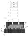
- FIG. 3 An embodiment of a method according to the present invention is schematically illustrated in Figure 3 .
- the embodiment of the method illustrated therein comprises a first step S1 wherein a layer of an optoelectric active material is applied between a first electrode and a second electrode.
- This first electrode is usually the anode, as it can have a high work-function. This facilitates further processing steps. In some processes the cathode may be applied as the first electrode, for example in processes using doped small molecule OLED materials.
- the first step S1 comprises a first substep S11 of providing the first electrode e.g. at a substrate a second substep S12 of providing the layer of optoelectric active material and the third substep S13 of providing the second electrode.
- the first electrode e.g.
- the embodiment shown in Figure 3 further comprises a second step S2.
- the result of the first and the second step is shown in Figure 4 .
- a patterned electrically insulating layer structure 60 is applied at at least one of said electrodes 32, here the cathode. It is not necessary that the patterned electrically insulating layer structure 60 is applied directly upon said electrode.
- One or more intermediate layers may be applied at the at least one of said electrode.
- a semiconducting layer may be applied at the cathode 32 before applying the patterned electrically insulating layer structure.
- the patterned electrically insulating layer structure 60 that is deposited has openings 62 that leave free portions of the at least one of the electrodes, here the second electrode 32.
- the patterned electrically insulating layer structure 60 e.g. the layer may be applied as a continuous layer which is subsequently patterned, e.g. by etching or by imprinting.
- the layer may be directly applied in its patterned form, e.g. by printing.
- the layer is applied by evaporation, e.g. by a CVD process, such as thermal chemical vapour deposition (CVD), photo assisted chemical vapour deposition (PACVD), plasma enhanced chemical vapour deposition (PECVD), etc and patterned using a mask.
- CVD thermal chemical vapour deposition
- PAVD photo assisted chemical vapour deposition
- PECVD plasma enhanced chemical vapour deposition
- the embodiment further comprises a third step S3.
- This execution of this step S3 is shown in detail in Figure 5 , while its result is shown in Figure 6 .
- the intermediate product shown in Figure 4 is submerged in a bath comprising an ionic liquid 70.
- the electrolyte 70 is provided in the openings 62 of the patterned electrically insulating layer structure 60.
- a metallic layer 80 is deposited at the free portions of the second electrode 32 by electroplating from an ionic liquid 70.
- the electrode 32 to be provided with the metallic deposition is coupled to a negative pole of a battery 72.
- the positive pole of a battery is coupled to an auxiliary electrode 74.
- the ionic liquid may be rolled out over the surface and brought into contact with the auxiliary electrode 74.
- the metallic layer 80 that is deposited at the free portions of the second electrode 32 forms a metal structure 80.
- Figure 7A shows a detail of this structure according to 7A in Figure 7 .
- the metal structure 80 is deposited directly at the free portions of the second electrode 32 (shown in fig. 6 ).
- the metal deposition process may continue until the metal structure 80 has a height h in the order of a few ⁇ m to a few tens of ⁇ m, e.g.
- the metal structure may have grooves having a width in the order of 50 to 100 ⁇ m that are mutually spaced at a distance of a few mm. Taking into account that the metal structure grows substantially isotropically, the structure will have a width w in the range of 70 to 120 ⁇ m in this example and a pitch P of a few mm, e.g. 3 mm as is shown schematically in Figure 7A .
- the metal structure 80 herewith is substantially invisible to the human eye and will only absorb a minor fraction of radiation generated by the optoelectric device in case of an OLED or of in case of an photovoltaic device, radiation impingent from the environment.
- a hexagonal structure as shown in Figures 7, 7A
- other structures may be used, e.g. the rectangular structure of Figure 7B .
- Step S3 may be followed by a further step S5, wherein a barrier layer structure 90 is applied on top of the metallic layer.
- the barrier layer structure 90 may comprise a sequence of inorganic layers, such as the sequence SiN,SiO,SiN,SiO,SiN, also denoted as NONON.
- the structure may comprise a sequence of alternating organic and inorganic layers, e.g. an organic layer that is sandwiched between a first and a second inorganic layer.
- the patterned electrically insulating layer structure may also comprise such sequence of inorganic layers or inorganic layers and organic layers.
- the barrier layer structure 90 may be applied in addition to a barrier layer structure formed by the electrically insulating layer structure 60. Alternatively, when a barrier layer structure 90 is applied the electrically insulating layer structure 60 does not need to have a barrier function. In that case for example a single layer of an organic material may be used for the electrically insulating layer structure 60.
- the metal structure 80 may be used as a contact to a further optoelectric device that is applied upon the optoelectric device formed by steps S1-S3 as shown in Figure 6 .
- a further layer of an optoelectric active material 110 is sandwiched between a first further electrode 122, which is formed by a further electrically conductive layer 120, and a second further electrode 132.
- This second further electrode 132 is electrically connected to a portion 124 of the further electrically conductive layer 120.
- the optoelectric active material may be an organic or an inorganic material. Organic materials have the advantage that they can be processed at a low temperature.
- the first further electrode 122 is applied at the patterned electrically insulating layer structure 60 with the metallic layer 80.
- steps S2 and S3 may be repeated so that also the further optoelectric device has a shunt structure.
- the process described in fig 9 can be repeated several times and also several different electro-optical devices can stacked on top of each other.
- both the layer 10 of an organic optoelectric active material and the further layer 110 of an optoelectric active material are a light-emitting layer.
- two light emitting devices are arranged in series, therewith enabling a doubling of the light-output with the same supply current. If desired more light emitting devices may be stacked in this way.
- hybrid optoelectric devices may be constructed in this way.
- the layer 10 is a light-emitting layer and the further layer 110 is a photo-voltaic layer.
- the layer 10 is a light-emitting layer and the further layer 110 is an electrochromic layer.
- the second and the third variant are particularly suitable in a window pane or a signage device.
- the second variant can be used at day-time in a first mode as an energy source that converts a part of the incoming light in electric energy, therewith at the same time tempering the intensity of the incoming light.
- the pane can be used in a second mode as a light source.
- the light emitting layer 10 may be patterned, e.g.
- the metallic layer 120 is efficiently used as it serves as common electric supply conductor. In the first mode it serves as a power supply line from the photo-voltaic layer 110 to outside the pane. In the second mode it serves as a power supply line towards the light-emitting layer 10.
- the electrochromic layer 110 allows for a more controllable tempering of the incoming light, as compared to a photo-voltaic layer.
- the combination of electrochromic layer 110 and the light-emitting layer 10 make it possible provide a window pane that provides for a controllable amount of light, e.g. to supply a constant intensity regardless the time of the day.
- the metallic layer 120 serves as common electric supply conductor, in this case for the light-emitting layer 10 and for the electrochromic layer 110.
Landscapes
- Physics & Mathematics (AREA)
- Optics & Photonics (AREA)
- Engineering & Computer Science (AREA)
- Manufacturing & Machinery (AREA)
- Chemical & Material Sciences (AREA)
- Life Sciences & Earth Sciences (AREA)
- Inorganic Chemistry (AREA)
- Sustainable Development (AREA)
- Electroluminescent Light Sources (AREA)
- Photovoltaic Devices (AREA)
- Composite Materials (AREA)
Priority Applications (8)
| Application Number | Priority Date | Filing Date | Title |
|---|---|---|---|
| EP09158618A EP2244317A1 (de) | 2009-04-23 | 2009-04-23 | Optoelektrische Vorrichtung und Verfahren zu deren Herstellung |
| US13/265,855 US20120074454A1 (en) | 2009-04-23 | 2010-04-23 | Optoelectric device and method for manufacturing the same |
| PCT/NL2010/050221 WO2010123362A1 (en) | 2009-04-23 | 2010-04-23 | Optoelectric device and method for manufacturing the same |
| KR1020117027970A KR20120028887A (ko) | 2009-04-23 | 2010-04-23 | 광전 소자 및 그의 제조 방법 |
| EP10718308.9A EP2422383B1 (de) | 2009-04-23 | 2010-04-23 | Optoelektrische einrichtung und verfahren zu ihrer herstellung |
| JP2012507172A JP5656975B2 (ja) | 2009-04-23 | 2010-04-23 | 光電デバイスおよびその製造方法 |
| CN201080022739.2A CN102439751B (zh) | 2009-04-23 | 2010-04-23 | 光电装置以及制造所述光电装置的方法 |
| US14/218,276 US20140197424A1 (en) | 2009-04-23 | 2014-03-18 | Optoelectric device and method for manufacturing the same |
Applications Claiming Priority (1)
| Application Number | Priority Date | Filing Date | Title |
|---|---|---|---|
| EP09158618A EP2244317A1 (de) | 2009-04-23 | 2009-04-23 | Optoelektrische Vorrichtung und Verfahren zu deren Herstellung |
Publications (1)
| Publication Number | Publication Date |
|---|---|
| EP2244317A1 true EP2244317A1 (de) | 2010-10-27 |
Family
ID=40849043
Family Applications (2)
| Application Number | Title | Priority Date | Filing Date |
|---|---|---|---|
| EP09158618A Withdrawn EP2244317A1 (de) | 2009-04-23 | 2009-04-23 | Optoelektrische Vorrichtung und Verfahren zu deren Herstellung |
| EP10718308.9A Not-in-force EP2422383B1 (de) | 2009-04-23 | 2010-04-23 | Optoelektrische einrichtung und verfahren zu ihrer herstellung |
Family Applications After (1)
| Application Number | Title | Priority Date | Filing Date |
|---|---|---|---|
| EP10718308.9A Not-in-force EP2422383B1 (de) | 2009-04-23 | 2010-04-23 | Optoelektrische einrichtung und verfahren zu ihrer herstellung |
Country Status (6)
| Country | Link |
|---|---|
| US (2) | US20120074454A1 (de) |
| EP (2) | EP2244317A1 (de) |
| JP (1) | JP5656975B2 (de) |
| KR (1) | KR20120028887A (de) |
| CN (1) | CN102439751B (de) |
| WO (1) | WO2010123362A1 (de) |
Families Citing this family (7)
| Publication number | Priority date | Publication date | Assignee | Title |
|---|---|---|---|---|
| GB0920986D0 (en) * | 2009-12-01 | 2010-01-13 | Lumicure Ltd | Substrate patterning |
| DE102012222760A1 (de) | 2012-12-11 | 2014-06-12 | Osram Opto Semiconductors Gmbh | Abdunkelbare spiegelvorrichtung |
| KR101407590B1 (ko) * | 2012-11-19 | 2014-06-13 | 삼성디스플레이 주식회사 | 유기 발광 표시 장치 및 그 제조방법 |
| KR102651543B1 (ko) * | 2015-12-10 | 2024-03-28 | 삼성전자주식회사 | 광 전자 장치와 이를 포함하는 스마트 윈도우 |
| GB2547029B (en) * | 2016-02-05 | 2019-11-06 | Cambridge Display Tech Ltd | Methods of manufacturing electrodes by in-situ electrodeposition and devices comprising said electrodes |
| WO2017133104A1 (zh) * | 2016-02-06 | 2017-08-10 | 无锡威迪变色玻璃有限公司 | 电致变色结构及其形成方法 |
| CN108615751A (zh) * | 2018-05-30 | 2018-10-02 | 信利光电股份有限公司 | 一种显示模组 |
Citations (6)
| Publication number | Priority date | Publication date | Assignee | Title |
|---|---|---|---|---|
| US20030043316A1 (en) * | 2000-11-29 | 2003-03-06 | International Business Machines Corporation | Three level stacked reflective display |
| DE10258712A1 (de) * | 2002-12-12 | 2004-07-22 | Samsung SDI Co., Ltd., Suwon | Bauelement für ein Aktiv-Matrix-OLED-Display mit integrierter Energieerzeugung |
| WO2007036850A2 (en) | 2005-09-28 | 2007-04-05 | Koninklijke Philips Electronics N.V. | A large area organic diode device and a method of manufacturing it |
| EP1801881A1 (de) * | 2005-12-21 | 2007-06-27 | Samsung SDI Co., Ltd. | Organische lichtemittierende Anzeige die an einer oder beiden Oberflächen ein Bild darstellen kann |
| EP1876657A1 (de) * | 2006-07-07 | 2008-01-09 | CSEM Centre Suisse d'Electronique et de Microtechnique SA | Verfahren zur Herstellung strukturierter Leiterschichten |
| EP1983592A1 (de) * | 2007-04-17 | 2008-10-22 | Nederlandse Organisatie voor Toegepast-Natuuurwetenschappelijk Onderzoek TNO | Verfahren zur Herstellung einer Elektrode |
Family Cites Families (11)
| Publication number | Priority date | Publication date | Assignee | Title |
|---|---|---|---|---|
| US6975067B2 (en) * | 2002-12-19 | 2005-12-13 | 3M Innovative Properties Company | Organic electroluminescent device and encapsulation method |
| US6812637B2 (en) * | 2003-03-13 | 2004-11-02 | Eastman Kodak Company | OLED display with auxiliary electrode |
| US7250728B2 (en) * | 2004-04-21 | 2007-07-31 | Au Optronics | Bottom and top emission OLED pixel structure |
| JP4027914B2 (ja) * | 2004-05-21 | 2007-12-26 | 株式会社半導体エネルギー研究所 | 照明装置及びそれを用いた機器 |
| US20070132371A1 (en) * | 2005-12-12 | 2007-06-14 | General Electric Company | Color tunable light-emitting devices and method of making the same |
| US20070131949A1 (en) * | 2005-12-12 | 2007-06-14 | General Electric Company | Color tunable light-emitting devices and method of making the same |
| GB2437112B (en) * | 2006-04-11 | 2011-04-13 | Nicholas Jim Stone | A method of making an electrical device |
| DE102007004509A1 (de) * | 2006-11-23 | 2008-05-29 | Fraunhofer-Gesellschaft zur Förderung der angewandten Forschung e.V. | Beleuchtungselement und Verfahren zu seiner Herstellung |
| EP1983079A1 (de) * | 2007-04-17 | 2008-10-22 | Nederlandse Organisatie voor Toegepast-Natuuurwetenschappelijk Onderzoek TNO | Barriereschicht und Herstellungsverfahren dafür |
| US20090079345A1 (en) * | 2007-09-26 | 2009-03-26 | Fujifilm Corporation | Light emitting/receiving element |
| JP2009081298A (ja) * | 2007-09-26 | 2009-04-16 | Fujifilm Corp | 撮像素子及び撮像装置 |
-
2009
- 2009-04-23 EP EP09158618A patent/EP2244317A1/de not_active Withdrawn
-
2010
- 2010-04-23 WO PCT/NL2010/050221 patent/WO2010123362A1/en not_active Ceased
- 2010-04-23 US US13/265,855 patent/US20120074454A1/en not_active Abandoned
- 2010-04-23 EP EP10718308.9A patent/EP2422383B1/de not_active Not-in-force
- 2010-04-23 CN CN201080022739.2A patent/CN102439751B/zh not_active Expired - Fee Related
- 2010-04-23 KR KR1020117027970A patent/KR20120028887A/ko not_active Abandoned
- 2010-04-23 JP JP2012507172A patent/JP5656975B2/ja not_active Expired - Fee Related
-
2014
- 2014-03-18 US US14/218,276 patent/US20140197424A1/en not_active Abandoned
Patent Citations (6)
| Publication number | Priority date | Publication date | Assignee | Title |
|---|---|---|---|---|
| US20030043316A1 (en) * | 2000-11-29 | 2003-03-06 | International Business Machines Corporation | Three level stacked reflective display |
| DE10258712A1 (de) * | 2002-12-12 | 2004-07-22 | Samsung SDI Co., Ltd., Suwon | Bauelement für ein Aktiv-Matrix-OLED-Display mit integrierter Energieerzeugung |
| WO2007036850A2 (en) | 2005-09-28 | 2007-04-05 | Koninklijke Philips Electronics N.V. | A large area organic diode device and a method of manufacturing it |
| EP1801881A1 (de) * | 2005-12-21 | 2007-06-27 | Samsung SDI Co., Ltd. | Organische lichtemittierende Anzeige die an einer oder beiden Oberflächen ein Bild darstellen kann |
| EP1876657A1 (de) * | 2006-07-07 | 2008-01-09 | CSEM Centre Suisse d'Electronique et de Microtechnique SA | Verfahren zur Herstellung strukturierter Leiterschichten |
| EP1983592A1 (de) * | 2007-04-17 | 2008-10-22 | Nederlandse Organisatie voor Toegepast-Natuuurwetenschappelijk Onderzoek TNO | Verfahren zur Herstellung einer Elektrode |
Also Published As
| Publication number | Publication date |
|---|---|
| CN102439751A (zh) | 2012-05-02 |
| KR20120028887A (ko) | 2012-03-23 |
| EP2422383A1 (de) | 2012-02-29 |
| JP2012524973A (ja) | 2012-10-18 |
| CN102439751B (zh) | 2016-01-06 |
| JP5656975B2 (ja) | 2015-01-21 |
| US20140197424A1 (en) | 2014-07-17 |
| US20120074454A1 (en) | 2012-03-29 |
| EP2422383B1 (de) | 2016-11-30 |
| WO2010123362A1 (en) | 2010-10-28 |
Similar Documents
| Publication | Publication Date | Title |
|---|---|---|
| TWI553935B (zh) | 製備光電裝置之方法 | |
| US20140197424A1 (en) | Optoelectric device and method for manufacturing the same | |
| EP2483944B1 (de) | Verfahren zur herstellung einer monolithischen parallelen verbindungsstruktur einer optoelektronischen vorrichtung | |
| CN102576803B (zh) | 光电器件及其制造方法 | |
| KR20080032128A (ko) | 유기계 장치 및 그 제조 방법 | |
| KR20120125280A (ko) | 마스크 없이 oled 소자를 제조하는 방법 | |
| US8816335B2 (en) | Method for creating serially-connected OLED devices | |
| EP2510563B1 (de) | Elektrooptische Vorrichtung mit Elektrode, sowie Verfahren zur Herstellung der elektrooptischen Vorrichtung | |
| EP2382677B1 (de) | Elektrooptische vorrichtung und verfahren zu ihrer herstellung | |
| EP2249412A1 (de) | Organisches Halbleiterbauelement und Verfahren zu seiner Herstellung |
Legal Events
| Date | Code | Title | Description |
|---|---|---|---|
| PUAI | Public reference made under article 153(3) epc to a published international application that has entered the european phase |
Free format text: ORIGINAL CODE: 0009012 |
|
| AK | Designated contracting states |
Kind code of ref document: A1 Designated state(s): AT BE BG CH CY CZ DE DK EE ES FI FR GB GR HR HU IE IS IT LI LT LU LV MC MK MT NL NO PL PT RO SE SI SK TR |
|
| AX | Request for extension of the european patent |
Extension state: AL BA RS |
|
| STAA | Information on the status of an ep patent application or granted ep patent |
Free format text: STATUS: THE APPLICATION IS DEEMED TO BE WITHDRAWN |
|
| 18D | Application deemed to be withdrawn |
Effective date: 20110428 |