EP2244460B1 - Bildanordnung und system zu seiner herstellung - Google Patents
Bildanordnung und system zu seiner herstellung Download PDFInfo
- Publication number
- EP2244460B1 EP2244460B1 EP09711230.4A EP09711230A EP2244460B1 EP 2244460 B1 EP2244460 B1 EP 2244460B1 EP 09711230 A EP09711230 A EP 09711230A EP 2244460 B1 EP2244460 B1 EP 2244460B1
- Authority
- EP
- European Patent Office
- Prior art keywords
- case
- circuit board
- mid
- mounting
- lens
- Prior art date
- Legal status (The legal status is an assumption and is not a legal conclusion. Google has not performed a legal analysis and makes no representation as to the accuracy of the status listed.)
- Not-in-force
Links
Images


Classifications
-
- G—PHYSICS
- G02—OPTICS
- G02B—OPTICAL ELEMENTS, SYSTEMS OR APPARATUS
- G02B13/00—Optical objectives specially designed for the purposes specified below
- G02B13/001—Miniaturised objectives for electronic devices, e.g. portable telephones, webcams, PDAs, small digital cameras
- G02B13/0015—Miniaturised objectives for electronic devices, e.g. portable telephones, webcams, PDAs, small digital cameras characterised by the lens design
- G02B13/002—Miniaturised objectives for electronic devices, e.g. portable telephones, webcams, PDAs, small digital cameras characterised by the lens design having at least one aspherical surface
- G02B13/003—Miniaturised objectives for electronic devices, e.g. portable telephones, webcams, PDAs, small digital cameras characterised by the lens design having at least one aspherical surface having two lenses
-
- G—PHYSICS
- G03—PHOTOGRAPHY; CINEMATOGRAPHY; ANALOGOUS TECHNIQUES USING WAVES OTHER THAN OPTICAL WAVES; ELECTROGRAPHY; HOLOGRAPHY
- G03B—APPARATUS OR ARRANGEMENTS FOR TAKING PHOTOGRAPHS OR FOR PROJECTING OR VIEWING THEM; APPARATUS OR ARRANGEMENTS EMPLOYING ANALOGOUS TECHNIQUES USING WAVES OTHER THAN OPTICAL WAVES; ACCESSORIES THEREFOR
- G03B17/00—Details of cameras or camera bodies; Accessories therefor
- G03B17/02—Bodies
-
- H—ELECTRICITY
- H04—ELECTRIC COMMUNICATION TECHNIQUE
- H04N—PICTORIAL COMMUNICATION, e.g. TELEVISION
- H04N23/00—Cameras or camera modules comprising electronic image sensors; Control thereof
- H04N23/50—Constructional details
- H04N23/54—Mounting of pick-up tubes, electronic image sensors, deviation or focusing coils
-
- H—ELECTRICITY
- H04—ELECTRIC COMMUNICATION TECHNIQUE
- H04N—PICTORIAL COMMUNICATION, e.g. TELEVISION
- H04N23/00—Cameras or camera modules comprising electronic image sensors; Control thereof
- H04N23/57—Mechanical or electrical details of cameras or camera modules specially adapted for being embedded in other devices
-
- G—PHYSICS
- G02—OPTICS
- G02B—OPTICAL ELEMENTS, SYSTEMS OR APPARATUS
- G02B13/00—Optical objectives specially designed for the purposes specified below
- G02B13/001—Miniaturised objectives for electronic devices, e.g. portable telephones, webcams, PDAs, small digital cameras
-
- Y—GENERAL TAGGING OF NEW TECHNOLOGICAL DEVELOPMENTS; GENERAL TAGGING OF CROSS-SECTIONAL TECHNOLOGIES SPANNING OVER SEVERAL SECTIONS OF THE IPC; TECHNICAL SUBJECTS COVERED BY FORMER USPC CROSS-REFERENCE ART COLLECTIONS [XRACs] AND DIGESTS
- Y10—TECHNICAL SUBJECTS COVERED BY FORMER USPC
- Y10T—TECHNICAL SUBJECTS COVERED BY FORMER US CLASSIFICATION
- Y10T29/00—Metal working
- Y10T29/49—Method of mechanical manufacture
- Y10T29/49002—Electrical device making
- Y10T29/49117—Conductor or circuit manufacturing
- Y10T29/49124—On flat or curved insulated base, e.g., printed circuit, etc.
- Y10T29/4913—Assembling to base an electrical component, e.g., capacitor, etc.
Definitions
- the present invention relates to an imaging device and a method for manufacturing the same.
- imaging devices have been widely used, for example, in vehicles and mobile phones, and are required to be miniaturized as they become popular.
- an imaging device having an imaging element compactly mounted on a circuit board utilizing molded interconnect device (MID) method.
- MID molded interconnect device
- Patent Document 1 An imaging device of this type known in related art (refer to Patent Document 1, for example) which prevents electrical problems attributed to the condition of the joints between an MID and a circuit board being incomplete when mounting a relatively heavy lens such as a high performance wide-angle lens.
- an imaging device 10 disclosed in Patent Document 1 is provided with a lens 11 having a male thread section 11 a, a lens bracket 12 having the lens 11 mounted therein, a lens fixing nut 13, an imaging element 14 for converting the light passing through the lens 11 to an electrical signal, an MID 15 having the imaging element 14 mounted thereon, an MID mounting substrate 16 having the MID 15 mounted thereon, a plate spring 21 attached to the lens bracket 12, a lower case 22 constituting a part of a housing, and an upper case 23 engaged with the plate spring 21 that presses down the lens bracket 12 towards the lower case 22 as the upper case 23 is fixed to the lower case 22.
- a female thread section 12a for accepting the lens 11
- a guide groove 12b for positioning the MID 15 in a direction orthogonal to an optical axis of the lens 11 with respect to the lens bracket 12 as shown by an arrow 11A in the drawing when engaged with the MID 15, an engaging section 12c that engages with the MID mounting substrate 16, and a catch 12d for securing the plate spring 21 in place.
- an engaging section 23a that engages with the plate spring 21 as the upper case 23 is fixed to the lower case 22. Accordingly, when the upper case 23 is fixed to the lower case 22, the MID mounting substrate 16 is pressed by the lens bracket 12 and is fixed to the lower case 22 as the section 23a of the upper case 23 engages with the plate spring 21.
- the imaging device 10 in related art thus described is assembled in the following manufacturing process.
- the lens 11 attached with the lens fixing nut 13 is inserted to the lens bracket 12.
- the lens 11 attached with the fixing nut 13 and the lens bracket 12 become unified.
- the imaging element 14, the MID 15, and the MID mounting substrate 16 are fixed to one another to be unified.
- the plate spring 21 is then secured to the lens bracket 12 by latching the plate spring 21 to the catch 12d of the lens bracket 12.
- the lens bracket 12 is fitted with the MID 15 along the guide groove 12b, and is engaged with the MID mounting substrate 16 at the engaging section 12c of the lens bracket 12, determining the position of the MID 15 with respect to the lens bracket 12 in the direction orthogonal to the optical axis of the lens 11.
- the position of the lens 11 with respect to the imaging element 14 in the optical axis direction i.e., focus position
- the lens 11 is secured to the lens bracket 12 with the lens fixing nut 13.
- the imaging element 14, the MID 15, and the MID mounting substrate 16 fixed to the lens bracket 12 that is with the lens 11 fixed therein are then inserted to the lower case 22 as an internal component 20.
- Patent Document 1 Japanese Laid-Open Patent Publication No. 2007-102017 Further art is disclosed by the documents JP 2007-004068 and US 2003/137595
- JP 2007-004068 shows an imaging device manufacturing method.
- a camera module 1 includes a lens group 2, an imager 3 where light from the lens group 2 is imaged, a main substrate 4 which holds the imager 3, and a case 5 which holds the lens group 2 and the main substrate 4.
- a supporting member 24 extending in the optical axis direction of the lens group 2 is arranged in the case 5, and the main substrate 4 is held in the case 5 while being fixed on the side surface of the supporting member 24.
- the main substrate acts as a mounting plate 4 and can slide along supporting members 24. By evaluating the focus, the plate 4 is fixed in a desired position by soldering it to the supporting members.
- US 2003/137595 shows an image pickup device having a package 3 accommodating an image sensing device 4 integrally combined with an optical component holding member 8a holding an optical component for forming an image of an object on the surface of the image sensing device 4, with a certain positional relationship between the optical component and image sensing device in the X, Y and Z-directions being determined, by engaging an engagement step portion 15 with an engagement claw 16.
- a focal length adjusting spacer 19 is arranged between the package 3 and the optical component holding member 8a, and a biasing member 18 for biasing the optical component 10 toward the package 3 is provided between the image sensing device accommodating package 3 and the optical component 10. Spacers 19 are used to obtain a predetermined distance "b". A distance "a" between the surface of the image sensing device 4 and the surface of the seal glass 5 is measured in advance.
- an object of the present invention to provide an imaging device and a manufacturing method thereof that can simplify the manufacturing process facilitating its production, and prevent misalignment of optical axis of the lens thereof due to vibrations or the like.
- the optical axis of the lens can be prevented from being misaligned due to, for example, vibrations or the like.
- the imaging device according to the present invention since the first case is fixed to the second case while the circuit board mounted with the imaging element is being secured to the second case provided with the lens via the mounting means, the manufacturing process can be simplified. Furthermore, since the clearance between the lens and the light receiving plane of the imaging element can be adjusted by the adjustment member, the focus adjustment for the imaging device can also be simplified. Consequently, the imaging device according to the present invention can be easily manufactured.
- the imaging device has a structure of the mounting means being integrally formed with the second case.
- the mounting means is integrally formed with the second case, the circuit board mounted with the imaging element can be directly secured to the second case, and the optical axis of the lens can be prevented from being misaligned due to, for example, vibrations or the like.
- the mounting means is integrally formed with the second case, the manufacturing process can be simplified, thereby facilitating its production.
- a method for manufacturing an imaging device includes preparing a first case constituting a part of a case, a second case provided with a lens and constituting the case integrally with the first case, an imaging element for converting light passing through the lens into an electrical signal, a circuit board with the imaging element mounted thereon, mounting means for mounting the circuit board onto the second case, and an adjustment member provided between the circuit board and the mounting means for adjusting a clearance between the lens and a light receiving plane of the imaging element; mounting the circuit board onto the second case via the mounting means; and fixing the first case onto the second case, in which the mounting of the circuit board includes adjusting a clearance between the lens and the light receiving plane of the imaging element with the adjustment member when mounting the circuit board onto the second case via the mounting means.
- the imaging device can be manufactured that can prevent an optical axis of the lens from being misaligned due to vibrations or the like.
- the focus position is adjusted by the adjustment member when mounting the circuit board to the second case via the mounting means, the focus position can be adjusted by a simple step of merely placing the adjustment member, thereby facilitating the production of the imaging device.
- the present invention can provide an imaging device and a method for manufacturing the same which can simplify the manufacturing process facilitating its production and prevent the optical axis of the lens from being misaligned due to vibrations or the like.
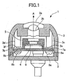
- FIG. 1 is a cross-sectional view of a vehicle-mounted camera 1 in accordance with the embodiment.
- the structure of the vehicle-mounted camera 1 will be described first.
- the vehicle-mounted camera 1 includes a lower case 2 constituting a part of a body case, an upper case 3 provided with lenses 3a and 3b and constituting the body case integrally with the lower case 2, an imaging element 4, an MID 5 with the imaging element 4 mounted thereon, an MID mounting substrate 6 with the MID 5 mounted thereon, two pieces of substrate mounting bosses 3c and 3d protruding from within the upper case 3 towards the MID mounting substrate 6, spacers 7a and 7b provided between the substrate mounting bosses 3c and 3d and the MID mounting substrate 6, and fixing screws 8a and 8b for securing the MID mounting substrate 6 to the substrate mounting bosses 3c and 3d.
- the lower case 2 and the upper case 3 are composed of resin or the like and constitute the body case of the vehicle-mounted camera 1 when fixed with each other.
- the lower case 2 and the upper case 3 constitute the first case and the second case of the present invention, respectively.
- a method using an ultrasonic welding can be used, for example.
- the resin or the like of the joint surfaces of the lower case 2 and the upper case 3 is completely fused, the body case of the vehicle-mounted camera 1 becomes highly air-tight, thereby making the vehicle-mounted camera 1 splash-proof.
- two pieces of the substrate mounting bosses 3c and 3d having respective end faces 3e and 3f and protruding from desired positions inside the upper case 3 are integrally formed.
- the number of substrate mounting bosses 3c and 3d are not limited to two, and three, four, or more of them may be used.
- the substrate mounting bosses 3c and 3d may be separate components not integrally formed with the upper case 3.
- the substrate mounting bosses 3c and 3d are adapted to secure the MID mounting substrate 6. The details of the substrate mounting bosses 3c and 3d will be described later.
- the lenses 3a and 3b are fixed being embedded in the upper case 3 and composed of glass or resin such as plastic, and are adapted to focus the light from the subject to form an image onto the imaging element 4. Since the lenses 3a and 3b are unified with the upper case 3, not as in the case of the vehicle-mounted camera in the related art in which the lenses and the upper case are separate, it is not necessary to provide any packing materials or the like to the joint portion of the lenses and the upper case, thereby simplifying the structure of the upper case 3.
- the imaging element 4 is mounted onto the MID 5 and is adapted to convert the light passing through the lenses 3a and 3b to an electrical signal.
- the MID 5 is adapted to mount the imaging element 4 as a three-dimensional circuit forming member and to be fixed onto the MID mounting substrate 6 and inserted between the substrate mounting bosses 3c and 3d with a predetermined clearance. More specifically, the MID 5 is fixed onto the MID mounting substrate 6 so that the position of a light receiving plane of the imaging element 4 comes to a desired position with respect to an optical axis of the lenses 3a and 3b.
- the MID mounting substrate 6 has mounting faces 6a and 6b with respective through-holes formed therein for passing through the fixing screws 8a and 8b, and is secured to the substrate mounting bosses 3c and 3d via the screws 8a and 8b through these holes.
- the MID mounting substrate 6 constitutes the circuit board of the invention.
- the spacers 7a and 7b are provided between the substrate mounting bosses 3c and 3d and the MID mounting substrate 6, and serve as adjustment members having a predetermined thickness for adjusting distances between the end faces 3e and 3f of the substrate mounting bosses 3c and 3d and the mounting faces 6a and 6b of the MID mounting substrate 6.
- the end faces 3e and 3f of the above-described substrate mounting bosses 3c and 3d are in parallel with a direction orthogonal to the optical axis of the lenses 3a and 3b, and have respective screw holes formed therein.
- the fixing screws 8a and 8b By tightening the fixing screws 8a and 8b to the screw holes of the end faces 3e and 3f, the MID mounting substrate 6 is fixed in a position parallel to the imaging element 4 and positioned in the direction orthogonal to the optical axis of the lenses 3a and 3b. Consequently, the position of the light receiving plane of the imaging element 4 is secured with respect to the optical axis of the lenses 3a and 3b.
- the substrate mounting bosses 3c and 3d and the fixing screws 8a and 8b constitute the mounting means of the present invention.
- the respective surfaces of the end faces 3e and 3f of the substrate mounting bosses 3c and 3d are not limited to be in parallel with the direction orthogonal to the optical axis of the lenses 3a and 3b
- Such an optimal focus position is detected in the following manner.
- a focus adjustment chart for example, is photographed as a photographing subject by the imaging element 4 through the lenses 3a and 3b, and the optimal focus position is detected based on the resolution of the focus adjustment chart photographed.
- the imaging element 4 photographs the focus adjustment chart. While the imaging element 4 is photographing the focus adjustment chart, with the end faces 3e and 3f of the substrate mounting bosses 3c and 3d as a reference plane where the mounting faces 6a and 6b of the MID mounting substrate 6 abut, the resolution is measured by varying a distance Z between the end faces 3e and 3f of the substrate mounting bosses 3c and 3d and the mounting surfaces of the MID mounting substrate 6 on substrate mounting bosses side, hereinafter referred to as "upper surface of the MID mounting substrate 6", in the direction of an arrow B.
- the resolution is measured by moving the MID mounting substrate 6 in the direction of optical axis of the lenses 3a and 3b.
- the relationship of the resolution of the focus adjustment chart photographed by the imaging element 4 with respect to the distance Z becomes as shown in FIG. 4 . It shows that, when the distance Z is not appropriate, the resolution of the focus adjustment chart photographed by the imaging element 4 becomes lower.
- FIGS. 2A to 2C are cross-sectional views of the vehicle-mounted camera 1 illustrating a part of its assembling process.
- the upper case 3 with the lenses 3a and 3b embedded is prepared in advance.
- the MID mounting substrate 6 having the MID 5 provided with the imaging element 4 mounted in advance is abutted to the end faces 3e and 3f of the substrate mounting bosses 3c and 3d formed in the upper case 3.
- the MID 5 mounted on the MID mounting substrate 6 is inserted, as described in the foregoing, between the two substrate mounting bosses 3c and 3d formed in the upper case 3.
- the spacers 7a and 7b that are set to a thickness corresponding to the distance Zo are inserted as the adjustment members between the end faces 3e and 3f of the substrate mounting bosses 3c and 3d and the upper surface of the MID mounting substrate 6.
- the MID mounting substrate 6 With the spacers 7a and 7b being inserted between the end faces 3e and 3f of the substrate mounting bosses 3c and 3d and the upper surface of the MID mounting substrate 6, the MID mounting substrate 6 is secured to the substrate mounting bosses 3c and 3d with the fixing screws 8a and 8b as securing means. This fixes the imaging element 4 to an appropriate focus position and completes the focus adjustment.
- the MID mounting substrate 6 is also appropriately positioned in the direction orthogonal to the optical axis of the lenses 3a and 3b.
- the above-described distance Zo of the optimal focus point differs from one vehicle-mounted camera to another because of the variances in position of the lenses, height of the MID, or the like. Accordingly, in the above focus adjustment, it is preferable that, with a plurality of spacers having different thicknesses in steps prepared in advance, the spacers of a thickness corresponding to the distance Zo be selected out of the plurality of spacers for each of the vehicle-mounted cameras.
- the spacers used in the above focus adjustment are not necessarily required to correspond precisely to the above-described distance Zo.
- the spacers may be selected from the spacers corresponding to a range of distance where the displacement of focus is in a tolerable degree that is, for example, allowable by depth of focus.
- the lower case 2 and the upper case 3 are bonded together by ultrasonic welding so as to make the case body of the vehicle-mounted camera 1 unified.
- the imaging element 4 can be prevented from being displaced not only with respect to the lenses 3a and 3b, but also with respect to the case body of the vehicle-mounted camera 1.
- the optical axis of the lenses is prevented from being displaced by vibrations or the like, thereby maintaining the imaging area in a default setting even when the vibrations or the like are exerted.
- the manufacturing process of the vehicle-mounted camera 1 can be simplified, thereby facilitating the production of the vehicle-mounted camera 1.
- the MID mounting substrate 6 is secured to the substrate mounting bosses 3c and 3d with the spacers 7a and 7b, the thicknesses of which correspond to the distance Zo of which the optimal focus position is obtainable, being inserted (i.e., interposed) between the end faces 3e and 3f of the substrate mounting bosses 3c and 3d and the upper surface of the MID mounting substrate 6, the focus adjustment process can be simplified.
- the lenses 3a and 3b are exemplified to be embedded in the upper case 3.
- the present invention is not limited to such a structure and, for example, it may be structured to mount a separate lens barrel provided with a group of lenses to the upper case 3 in a unified manner.
- the present invention is not limited as such.
- the present invention may also be applied, for example, to a circuit board that is mounted with a packaged imaging element.
- the imaging device and the manufacturing method thereof according to the present invention has advantages of simplifying the manufacturing process thereof facilitating its production, and preventing the optical axis of the lenses from being displaced due to vibrations or the like.
- the present invention is useful for an imaging device installed in a vehicle for taking an image of an object and for a manufacturing method thereof.
Landscapes
- Physics & Mathematics (AREA)
- Engineering & Computer Science (AREA)
- Multimedia (AREA)
- Signal Processing (AREA)
- General Physics & Mathematics (AREA)
- Optics & Photonics (AREA)
- Studio Devices (AREA)
- Camera Bodies And Camera Details Or Accessories (AREA)
Claims (2)
- Verfahren zur Herstellung einer Bildgebungsvorrichtung (1), umfassend ein zweites Gehäuse (3), in das eine Linsengruppe eingebettet ist, die aus einer Mehrzahl von Linsen (3a, 3b) besteht, und das ein Rumpfgehäuse aus einem Stück mit einem ersten Gehäuse (2) bildet, ein Bildgebungselement (4) zum Umwandeln eines Bildes, das durch die Linsengruppe erhalten wird, in ein elektrisches Signal, und eine Leiterplatte (6) mit dem Bildgebungselement (4) darauf montiert, wobei das zweite Gehäuse (3) Befestigungsmittel (3c, 3d), die aus einem Stück damit ausgebildet sind und von innerhalb des zweiten Gehäuses (3) in Richtung der Leiterplatte (6) vorstehen, zum Befestigen der Leiterplatte (6) daran aufweist, wobei die Befestigungsmittel (3c, 3d) eine Bezugsebene definieren, an welcher die Leiterplatte anliegt, umfassend:Fotografieren eines Fokuseinstellungsdiagramms,Anpassen eines Spielraums zwischen den Befestigungsmitteln und der Leiterplatte durch Vergrößern eines Abstands (Z) zwischen der Bezugsebene und einer Befestigungsfläche der Leiterplatte (6) in einer Spielraumposition (Z0), in der das Bildgebungselement (4) durch Bewegen der Leiterplatte in einer Richtung einer optischen Achse der Linsengruppe ein optimales Bild erhält, so dass die Auflösung des fotografierten Fokuseinstellungsdiagramms am höchsten wird;Einfügen eines Anpassungselements (7a, 7b) mit einer Dicke basierend auf der angepassten Spielraumposition (Z0), in der die Auflösung am höchsten ist, zwischen der Leiterplatte (6) und den Befestigungsmitteln (3c, 3d, 8a, 8b); undBefestigen der Leiterplatte (6) an den Befestigungsmitteln (3c, 3d) mit Befestigungsschrauben (8a, 8b).
- Verfahren zur Herstellung einer Bildgebungsvorrichtung nach Anspruch 1, ferner umfassend ein Auswählen des Anpassungselements (7a, 7b) basierend auf der angepassten Spielraumposition (Z0) aus einer Mehrzahl von Anpassungselementen (7a, 7b) mit verschiedenen Dicken, die im Voraus hergestellt werden.
Applications Claiming Priority (2)
| Application Number | Priority Date | Filing Date | Title |
|---|---|---|---|
| JP2008032033A JP2009194543A (ja) | 2008-02-13 | 2008-02-13 | 撮像装置およびその製造方法 |
| PCT/JP2009/000440 WO2009101774A1 (ja) | 2008-02-13 | 2009-02-05 | 撮像装置およびその製造方法 |
Publications (3)
| Publication Number | Publication Date |
|---|---|
| EP2244460A1 EP2244460A1 (de) | 2010-10-27 |
| EP2244460A4 EP2244460A4 (de) | 2011-11-02 |
| EP2244460B1 true EP2244460B1 (de) | 2015-04-01 |
Family
ID=40956809
Family Applications (1)
| Application Number | Title | Priority Date | Filing Date |
|---|---|---|---|
| EP09711230.4A Not-in-force EP2244460B1 (de) | 2008-02-13 | 2009-02-05 | Bildanordnung und system zu seiner herstellung |
Country Status (5)
| Country | Link |
|---|---|
| US (1) | US7979982B2 (de) |
| EP (1) | EP2244460B1 (de) |
| JP (1) | JP2009194543A (de) |
| CN (1) | CN101855898A (de) |
| WO (1) | WO2009101774A1 (de) |
Families Citing this family (13)
| Publication number | Priority date | Publication date | Assignee | Title |
|---|---|---|---|---|
| CN101493562A (zh) * | 2008-01-21 | 2009-07-29 | 鸿富锦精密工业(深圳)有限公司 | 镜筒旋入装置及镜筒定位方法 |
| JP2009194543A (ja) * | 2008-02-13 | 2009-08-27 | Panasonic Corp | 撮像装置およびその製造方法 |
| EP2451147A4 (de) | 2010-03-10 | 2012-12-05 | Smk Kk | Kameramodul |
| KR101376882B1 (ko) * | 2012-11-15 | 2014-03-20 | 삼성전기주식회사 | 차량용 카메라 |
| DE102013205160A1 (de) * | 2013-03-22 | 2014-09-25 | Robert Bosch Gmbh | Kamerasystem, insbesondere für ein Fahrzeug, und Verfahren zu dessen Herstellung |
| JP6583611B2 (ja) * | 2015-04-27 | 2019-10-02 | ミツミ電機株式会社 | カメラ装置の組立て方法およびレンズユニットの組立て方法 |
| CN106896463B (zh) * | 2015-12-17 | 2020-07-31 | 宁波舜宇车载光学技术有限公司 | 用于车载光学成像系统的光学镜头 |
| JP6667424B2 (ja) * | 2016-11-29 | 2020-03-18 | 日本電産コパル株式会社 | 撮像装置 |
| JP6827177B2 (ja) * | 2017-05-24 | 2021-02-10 | パナソニックIpマネジメント株式会社 | 車載カメラおよびその組立方法 |
| DE102017124550A1 (de) * | 2017-10-20 | 2019-04-25 | Connaught Electronics Ltd. | Kamera für ein Kraftfahrzeug mit zumindest zwei Leiterplatten und verbesserter elektromagnetischer Abschirmung, Kamerasystem, Kraftfahrzeug sowie Herstellungsverfahren |
| CN108650439B (zh) * | 2018-04-24 | 2023-06-02 | 东风商用车有限公司 | 一种安装姿态可调的车载摄像头总成及其姿态调整方法 |
| CN110769141B (zh) * | 2019-11-20 | 2024-06-07 | 浙江舜宇智领技术有限公司 | 一种车载摄像模组 |
| JP6896119B1 (ja) * | 2020-01-24 | 2021-06-30 | 三菱電機株式会社 | 車載カメラ |
Citations (1)
| Publication number | Priority date | Publication date | Assignee | Title |
|---|---|---|---|---|
| JP2006325100A (ja) * | 2005-05-20 | 2006-11-30 | Olympus Imaging Corp | デジタルカメラの調整方法及び、その調整装置 |
Family Cites Families (44)
| Publication number | Priority date | Publication date | Assignee | Title |
|---|---|---|---|---|
| US4866837A (en) * | 1987-12-03 | 1989-09-19 | Hughes Aircraft Company | Dual port alignment assembly station for attaching components to circuit boards |
| US5044072A (en) * | 1990-04-13 | 1991-09-03 | Air-Vac Engineering Company, Inc. | Vision system apparatus and method for component/pad alignment |
| US5194948A (en) * | 1991-04-26 | 1993-03-16 | At&T Bell Laboratories | Article alignment method and apparatus |
| US5152055A (en) * | 1991-04-26 | 1992-10-06 | At&T Bell Laboratories | Article alignment method |
| US5590456A (en) * | 1994-12-07 | 1997-01-07 | Lucent Technologies Inc. | Apparatus for precise alignment and placement of optoelectric components |
| JPH10321827A (ja) * | 1997-05-16 | 1998-12-04 | Sony Corp | 撮像装置及びカメラ |
| JPH11330798A (ja) * | 1998-05-19 | 1999-11-30 | Fuji Mach Mfg Co Ltd | 電気部品装着方法およびシステム |
| US6117193A (en) * | 1999-10-20 | 2000-09-12 | Amkor Technology, Inc. | Optical sensor array mounting and alignment |
| US6956615B2 (en) * | 2000-01-28 | 2005-10-18 | Pentax Corporation | Structure for mounting a solid-state imaging device |
| JP3607160B2 (ja) * | 2000-04-07 | 2005-01-05 | 三菱電機株式会社 | 撮像装置 |
| JP2002050896A (ja) * | 2000-08-03 | 2002-02-15 | Sony Corp | 部品把持位置補正装置および補正方法 |
| US6718626B2 (en) * | 2000-09-13 | 2004-04-13 | Fuji Machine Mfg. Co., Ltd. | Apparatus for detecting positioning error of a component with respect to a suction nozzle |
| US7059040B1 (en) * | 2001-01-16 | 2006-06-13 | Amkor Technology, Inc. | Optical module with lens integral holder fabrication method |
| JP2002247442A (ja) * | 2001-02-21 | 2002-08-30 | Matsushita Electric Ind Co Ltd | 撮像素子の取り付け角度調整機構 |
| JP3490694B2 (ja) * | 2001-03-28 | 2004-01-26 | 三菱電機株式会社 | 撮像装置及びその製造方法 |
| JP3613193B2 (ja) * | 2001-03-30 | 2005-01-26 | 三菱電機株式会社 | 撮像装置 |
| CN100394577C (zh) * | 2002-04-04 | 2008-06-11 | 东丽工程株式会社 | 定位方法及使用该方法的安装方法 |
| JP4190269B2 (ja) * | 2002-07-09 | 2008-12-03 | 新光電気工業株式会社 | 素子内蔵基板製造方法およびその装置 |
| JP2005534998A (ja) * | 2002-08-08 | 2005-11-17 | カール・ツァイス・エスエムティー・アーゲー | イメージングデバイスにおける光学式アセンブリを保持するための装置 |
| US7587803B2 (en) * | 2002-09-30 | 2009-09-15 | Tpo Displays Corp. | Method for assembling a camera module |
| US6762790B1 (en) * | 2002-12-20 | 2004-07-13 | Bendix Commercial Vehicle Systems Llc | Universal camera bracket that allows 180 degree of pitch adjustment |
| US7330211B2 (en) * | 2003-07-08 | 2008-02-12 | Micron Technology, Inc. | Camera module with focus adjustment structure and systems and methods of making the same |
| JP4405208B2 (ja) * | 2003-08-25 | 2010-01-27 | 株式会社ルネサステクノロジ | 固体撮像装置の製造方法 |
| US20050125993A1 (en) * | 2003-11-07 | 2005-06-16 | Madsen David D. | Pick and place machine with improved setup and operation procedure |
| JP2005164955A (ja) * | 2003-12-02 | 2005-06-23 | Fujitsu Ltd | 撮像デバイス、撮像デバイスの製造方法及び撮像デバイス保持機構 |
| JP2005345571A (ja) * | 2004-05-31 | 2005-12-15 | Canon Inc | 撮像装置および電子機器 |
| US7646075B2 (en) * | 2004-08-31 | 2010-01-12 | Micron Technology, Inc. | Microelectronic imagers having front side contacts |
| TWI312098B (en) * | 2005-01-03 | 2009-07-11 | Qisda Corporatio | Adjustable lens module and image projector applied with the lens module |
| JP4652149B2 (ja) * | 2005-06-27 | 2011-03-16 | 京セラ株式会社 | カメラモジュール |
| TWI289365B (en) * | 2005-09-29 | 2007-11-01 | Visera Technologies Co Ltd | Wafer scale image module |
| JP4755476B2 (ja) | 2005-10-06 | 2011-08-24 | パナソニック株式会社 | 撮像装置 |
| TWI370943B (en) * | 2005-10-28 | 2012-08-21 | Hon Hai Prec Ind Co Ltd | A digital camer lens |
| CN101292194B (zh) * | 2005-11-04 | 2012-07-11 | 松下电器产业株式会社 | 摄像装置及照相机 |
| DE102006013164A1 (de) * | 2006-03-22 | 2007-09-27 | Robert Bosch Gmbh | Verfahren zur Montage eines Kameramoduls und Kameramodul |
| CN100561285C (zh) * | 2006-04-07 | 2009-11-18 | 鸿富锦精密工业(深圳)有限公司 | 镜头模块 |
| US7433038B2 (en) * | 2006-04-27 | 2008-10-07 | Asml Netherlands B.V. | Alignment of substrates for bonding |
| KR100831710B1 (ko) * | 2006-08-17 | 2008-05-22 | 삼성전기주식회사 | 카메라 모듈의 조립 장치 및 그 조립 방법 |
| CN101206296B (zh) * | 2006-12-22 | 2010-05-19 | 鸿富锦精密工业(深圳)有限公司 | 镜头模组 |
| EP1944640A1 (de) * | 2007-01-11 | 2008-07-16 | STMicroelectronics (Research & Development) Limited | Linsenanordnung |
| US7928358B2 (en) * | 2007-02-08 | 2011-04-19 | Olympus Imaging Corp. | Imaging device module and portable electronic apparatus utilizing the same |
| CN101334511A (zh) * | 2007-06-29 | 2008-12-31 | 鸿富锦精密工业(深圳)有限公司 | 一种影像装置组装方法 |
| CN101843106B (zh) * | 2007-11-01 | 2015-11-25 | 柯尼卡美能达控股株式会社 | 摄像装置 |
| JP2009194543A (ja) * | 2008-02-13 | 2009-08-27 | Panasonic Corp | 撮像装置およびその製造方法 |
| JP2009244394A (ja) * | 2008-03-28 | 2009-10-22 | Fujinon Corp | レンズ組立体および撮像装置 |
-
2008
- 2008-02-13 JP JP2008032033A patent/JP2009194543A/ja active Pending
-
2009
- 2009-02-05 CN CN200980100943A patent/CN101855898A/zh active Pending
- 2009-02-05 WO PCT/JP2009/000440 patent/WO2009101774A1/ja not_active Ceased
- 2009-02-05 EP EP09711230.4A patent/EP2244460B1/de not_active Not-in-force
- 2009-02-05 US US12/681,825 patent/US7979982B2/en active Active
Patent Citations (1)
| Publication number | Priority date | Publication date | Assignee | Title |
|---|---|---|---|---|
| JP2006325100A (ja) * | 2005-05-20 | 2006-11-30 | Olympus Imaging Corp | デジタルカメラの調整方法及び、その調整装置 |
Also Published As
| Publication number | Publication date |
|---|---|
| CN101855898A (zh) | 2010-10-06 |
| EP2244460A4 (de) | 2011-11-02 |
| US7979982B2 (en) | 2011-07-19 |
| WO2009101774A1 (ja) | 2009-08-20 |
| EP2244460A1 (de) | 2010-10-27 |
| JP2009194543A (ja) | 2009-08-27 |
| US20100236063A1 (en) | 2010-09-23 |
Similar Documents
| Publication | Publication Date | Title |
|---|---|---|
| EP2244460B1 (de) | Bildanordnung und system zu seiner herstellung | |
| JP5771901B2 (ja) | 撮像装置 | |
| JP4378434B2 (ja) | 複眼カメラモジュール | |
| JP4527140B2 (ja) | 車載カメラ装置 | |
| US9888157B2 (en) | Lens mounting mechanism, lens mounting method, and image pickup device | |
| KR20200011560A (ko) | 카메라 렌즈 모듈 및 그 제조 방법 | |
| JP7205486B2 (ja) | 撮像装置 | |
| US20030137595A1 (en) | Image pickup device and camera | |
| JP2011215183A (ja) | 撮像装置 | |
| US20100259655A1 (en) | Imaging device | |
| JP6657099B2 (ja) | 撮像装置、光学機器、電子機器および車両 | |
| EP2659225B1 (de) | Sortiervorrichtung | |
| US20140362285A1 (en) | Lens module and method for manufacturing lens module | |
| JP2012114675A (ja) | 撮像装置 | |
| KR20060104949A (ko) | 광학 장치 모듈, 및 광학 장치 모듈의 제조 방법 | |
| JP6967424B2 (ja) | 撮像装置 | |
| US8259224B2 (en) | Method of setting position of imaging device | |
| JP4755476B2 (ja) | 撮像装置 | |
| KR101598221B1 (ko) | 카메라모듈 | |
| JP2010041373A (ja) | カメラモジュールおよびステレオカメラ | |
| JP7817025B2 (ja) | 測距装置、および移動体 | |
| JP4765443B2 (ja) | 鏡胴間部材の固定方法およびレンズユニット並びに撮像装置 | |
| US20250088724A1 (en) | Optical apparatus, vehicle-mounted camera, and transportation apparatus | |
| JP6261870B2 (ja) | カメラ装置 | |
| JP2006067147A (ja) | 固体撮像装置 |
Legal Events
| Date | Code | Title | Description |
|---|---|---|---|
| PUAI | Public reference made under article 153(3) epc to a published international application that has entered the european phase |
Free format text: ORIGINAL CODE: 0009012 |
|
| 17P | Request for examination filed |
Effective date: 20100312 |
|
| AK | Designated contracting states |
Kind code of ref document: A1 Designated state(s): AT BE BG CH CY CZ DE DK EE ES FI FR GB GR HR HU IE IS IT LI LT LU LV MC MK MT NL NO PL PT RO SE SI SK TR |
|
| AX | Request for extension of the european patent |
Extension state: AL BA RS |
|
| DAX | Request for extension of the european patent (deleted) | ||
| A4 | Supplementary search report drawn up and despatched |
Effective date: 20111006 |
|
| RIC1 | Information provided on ipc code assigned before grant |
Ipc: H04N 5/225 20060101AFI20110929BHEP Ipc: G02B 7/02 20060101ALI20110929BHEP Ipc: G02B 13/00 20060101ALI20110929BHEP Ipc: G03B 17/02 20060101ALI20110929BHEP |
|
| 17Q | First examination report despatched |
Effective date: 20140213 |
|
| GRAP | Despatch of communication of intention to grant a patent |
Free format text: ORIGINAL CODE: EPIDOSNIGR1 |
|
| INTG | Intention to grant announced |
Effective date: 20150107 |
|
| GRAS | Grant fee paid |
Free format text: ORIGINAL CODE: EPIDOSNIGR3 |
|
| GRAA | (expected) grant |
Free format text: ORIGINAL CODE: 0009210 |
|
| RAP1 | Party data changed (applicant data changed or rights of an application transferred) |
Owner name: PANASONIC INTELLECTUAL PROPERTY MANAGEMENT CO., LT |
|
| RAP1 | Party data changed (applicant data changed or rights of an application transferred) |
Owner name: PANASONIC INTELLECTUAL PROPERTY MANAGEMENT CO., LT |
|
| AK | Designated contracting states |
Kind code of ref document: B1 Designated state(s): AT BE BG CH CY CZ DE DK EE ES FI FR GB GR HR HU IE IS IT LI LT LU LV MC MK MT NL NO PL PT RO SE SI SK TR |
|
| REG | Reference to a national code |
Ref country code: GB Ref legal event code: FG4D |
|
| REG | Reference to a national code |
Ref country code: CH Ref legal event code: EP |
|
| REG | Reference to a national code |
Ref country code: IE Ref legal event code: FG4D |
|
| REG | Reference to a national code |
Ref country code: DE Ref legal event code: R096 Ref document number: 602009030322 Country of ref document: DE Effective date: 20150513 |
|
| REG | Reference to a national code |
Ref country code: AT Ref legal event code: REF Ref document number: 719696 Country of ref document: AT Kind code of ref document: T Effective date: 20150515 |
|
| REG | Reference to a national code |
Ref country code: NL Ref legal event code: VDEP Effective date: 20150401 |
|
| REG | Reference to a national code |
Ref country code: AT Ref legal event code: MK05 Ref document number: 719696 Country of ref document: AT Kind code of ref document: T Effective date: 20150401 |
|
| REG | Reference to a national code |
Ref country code: LT Ref legal event code: MG4D |
|
| PG25 | Lapsed in a contracting state [announced via postgrant information from national office to epo] |
Ref country code: NL Free format text: LAPSE BECAUSE OF FAILURE TO SUBMIT A TRANSLATION OF THE DESCRIPTION OR TO PAY THE FEE WITHIN THE PRESCRIBED TIME-LIMIT Effective date: 20150401 |
|
| PG25 | Lapsed in a contracting state [announced via postgrant information from national office to epo] |
Ref country code: HR Free format text: LAPSE BECAUSE OF FAILURE TO SUBMIT A TRANSLATION OF THE DESCRIPTION OR TO PAY THE FEE WITHIN THE PRESCRIBED TIME-LIMIT Effective date: 20150401 Ref country code: ES Free format text: LAPSE BECAUSE OF FAILURE TO SUBMIT A TRANSLATION OF THE DESCRIPTION OR TO PAY THE FEE WITHIN THE PRESCRIBED TIME-LIMIT Effective date: 20150401 Ref country code: FI Free format text: LAPSE BECAUSE OF FAILURE TO SUBMIT A TRANSLATION OF THE DESCRIPTION OR TO PAY THE FEE WITHIN THE PRESCRIBED TIME-LIMIT Effective date: 20150401 Ref country code: NO Free format text: LAPSE BECAUSE OF FAILURE TO SUBMIT A TRANSLATION OF THE DESCRIPTION OR TO PAY THE FEE WITHIN THE PRESCRIBED TIME-LIMIT Effective date: 20150701 Ref country code: CZ Free format text: LAPSE BECAUSE OF FAILURE TO SUBMIT A TRANSLATION OF THE DESCRIPTION OR TO PAY THE FEE WITHIN THE PRESCRIBED TIME-LIMIT Effective date: 20150401 Ref country code: PT Free format text: LAPSE BECAUSE OF FAILURE TO SUBMIT A TRANSLATION OF THE DESCRIPTION OR TO PAY THE FEE WITHIN THE PRESCRIBED TIME-LIMIT Effective date: 20150803 Ref country code: LT Free format text: LAPSE BECAUSE OF FAILURE TO SUBMIT A TRANSLATION OF THE DESCRIPTION OR TO PAY THE FEE WITHIN THE PRESCRIBED TIME-LIMIT Effective date: 20150401 |
|
| PG25 | Lapsed in a contracting state [announced via postgrant information from national office to epo] |
Ref country code: AT Free format text: LAPSE BECAUSE OF FAILURE TO SUBMIT A TRANSLATION OF THE DESCRIPTION OR TO PAY THE FEE WITHIN THE PRESCRIBED TIME-LIMIT Effective date: 20150401 Ref country code: LV Free format text: LAPSE BECAUSE OF FAILURE TO SUBMIT A TRANSLATION OF THE DESCRIPTION OR TO PAY THE FEE WITHIN THE PRESCRIBED TIME-LIMIT Effective date: 20150401 Ref country code: IS Free format text: LAPSE BECAUSE OF FAILURE TO SUBMIT A TRANSLATION OF THE DESCRIPTION OR TO PAY THE FEE WITHIN THE PRESCRIBED TIME-LIMIT Effective date: 20150801 Ref country code: GR Free format text: LAPSE BECAUSE OF FAILURE TO SUBMIT A TRANSLATION OF THE DESCRIPTION OR TO PAY THE FEE WITHIN THE PRESCRIBED TIME-LIMIT Effective date: 20150702 |
|
| REG | Reference to a national code |
Ref country code: DE Ref legal event code: R097 Ref document number: 602009030322 Country of ref document: DE |
|
| PG25 | Lapsed in a contracting state [announced via postgrant information from national office to epo] |
Ref country code: EE Free format text: LAPSE BECAUSE OF FAILURE TO SUBMIT A TRANSLATION OF THE DESCRIPTION OR TO PAY THE FEE WITHIN THE PRESCRIBED TIME-LIMIT Effective date: 20150401 Ref country code: DK Free format text: LAPSE BECAUSE OF FAILURE TO SUBMIT A TRANSLATION OF THE DESCRIPTION OR TO PAY THE FEE WITHIN THE PRESCRIBED TIME-LIMIT Effective date: 20150401 |
|
| PLBE | No opposition filed within time limit |
Free format text: ORIGINAL CODE: 0009261 |
|
| STAA | Information on the status of an ep patent application or granted ep patent |
Free format text: STATUS: NO OPPOSITION FILED WITHIN TIME LIMIT |
|
| REG | Reference to a national code |
Ref country code: FR Ref legal event code: PLFP Year of fee payment: 8 |
|
| PG25 | Lapsed in a contracting state [announced via postgrant information from national office to epo] |
Ref country code: PL Free format text: LAPSE BECAUSE OF FAILURE TO SUBMIT A TRANSLATION OF THE DESCRIPTION OR TO PAY THE FEE WITHIN THE PRESCRIBED TIME-LIMIT Effective date: 20150401 Ref country code: RO Free format text: LAPSE BECAUSE OF NON-PAYMENT OF DUE FEES Effective date: 20150401 Ref country code: SK Free format text: LAPSE BECAUSE OF FAILURE TO SUBMIT A TRANSLATION OF THE DESCRIPTION OR TO PAY THE FEE WITHIN THE PRESCRIBED TIME-LIMIT Effective date: 20150401 |
|
| 26N | No opposition filed |
Effective date: 20160105 |
|
| PG25 | Lapsed in a contracting state [announced via postgrant information from national office to epo] |
Ref country code: SI Free format text: LAPSE BECAUSE OF FAILURE TO SUBMIT A TRANSLATION OF THE DESCRIPTION OR TO PAY THE FEE WITHIN THE PRESCRIBED TIME-LIMIT Effective date: 20150401 Ref country code: BE Free format text: LAPSE BECAUSE OF NON-PAYMENT OF DUE FEES Effective date: 20160229 |
|
| PG25 | Lapsed in a contracting state [announced via postgrant information from national office to epo] |
Ref country code: BE Free format text: LAPSE BECAUSE OF FAILURE TO SUBMIT A TRANSLATION OF THE DESCRIPTION OR TO PAY THE FEE WITHIN THE PRESCRIBED TIME-LIMIT Effective date: 20150401 |
|
| PG25 | Lapsed in a contracting state [announced via postgrant information from national office to epo] |
Ref country code: LU Free format text: LAPSE BECAUSE OF FAILURE TO SUBMIT A TRANSLATION OF THE DESCRIPTION OR TO PAY THE FEE WITHIN THE PRESCRIBED TIME-LIMIT Effective date: 20160205 Ref country code: MC Free format text: LAPSE BECAUSE OF FAILURE TO SUBMIT A TRANSLATION OF THE DESCRIPTION OR TO PAY THE FEE WITHIN THE PRESCRIBED TIME-LIMIT Effective date: 20150401 |
|
| REG | Reference to a national code |
Ref country code: CH Ref legal event code: PL |
|
| PG25 | Lapsed in a contracting state [announced via postgrant information from national office to epo] |
Ref country code: LI Free format text: LAPSE BECAUSE OF NON-PAYMENT OF DUE FEES Effective date: 20160229 Ref country code: CH Free format text: LAPSE BECAUSE OF NON-PAYMENT OF DUE FEES Effective date: 20160229 |
|
| REG | Reference to a national code |
Ref country code: IE Ref legal event code: MM4A |
|
| PG25 | Lapsed in a contracting state [announced via postgrant information from national office to epo] |
Ref country code: IE Free format text: LAPSE BECAUSE OF NON-PAYMENT OF DUE FEES Effective date: 20160205 |
|
| REG | Reference to a national code |
Ref country code: FR Ref legal event code: PLFP Year of fee payment: 9 |
|
| PG25 | Lapsed in a contracting state [announced via postgrant information from national office to epo] |
Ref country code: SE Free format text: LAPSE BECAUSE OF FAILURE TO SUBMIT A TRANSLATION OF THE DESCRIPTION OR TO PAY THE FEE WITHIN THE PRESCRIBED TIME-LIMIT Effective date: 20150401 |
|
| PG25 | Lapsed in a contracting state [announced via postgrant information from national office to epo] |
Ref country code: MT Free format text: LAPSE BECAUSE OF FAILURE TO SUBMIT A TRANSLATION OF THE DESCRIPTION OR TO PAY THE FEE WITHIN THE PRESCRIBED TIME-LIMIT Effective date: 20150401 |
|
| REG | Reference to a national code |
Ref country code: FR Ref legal event code: PLFP Year of fee payment: 10 |
|
| PG25 | Lapsed in a contracting state [announced via postgrant information from national office to epo] |
Ref country code: HU Free format text: LAPSE BECAUSE OF FAILURE TO SUBMIT A TRANSLATION OF THE DESCRIPTION OR TO PAY THE FEE WITHIN THE PRESCRIBED TIME-LIMIT; INVALID AB INITIO Effective date: 20090205 Ref country code: CY Free format text: LAPSE BECAUSE OF FAILURE TO SUBMIT A TRANSLATION OF THE DESCRIPTION OR TO PAY THE FEE WITHIN THE PRESCRIBED TIME-LIMIT Effective date: 20150401 |
|
| PGFP | Annual fee paid to national office [announced via postgrant information from national office to epo] |
Ref country code: IT Payment date: 20180227 Year of fee payment: 10 |
|
| PG25 | Lapsed in a contracting state [announced via postgrant information from national office to epo] |
Ref country code: MT Free format text: LAPSE BECAUSE OF FAILURE TO SUBMIT A TRANSLATION OF THE DESCRIPTION OR TO PAY THE FEE WITHIN THE PRESCRIBED TIME-LIMIT Effective date: 20160229 Ref country code: TR Free format text: LAPSE BECAUSE OF FAILURE TO SUBMIT A TRANSLATION OF THE DESCRIPTION OR TO PAY THE FEE WITHIN THE PRESCRIBED TIME-LIMIT Effective date: 20150401 Ref country code: MK Free format text: LAPSE BECAUSE OF FAILURE TO SUBMIT A TRANSLATION OF THE DESCRIPTION OR TO PAY THE FEE WITHIN THE PRESCRIBED TIME-LIMIT Effective date: 20150401 |
|
| PG25 | Lapsed in a contracting state [announced via postgrant information from national office to epo] |
Ref country code: BG Free format text: LAPSE BECAUSE OF FAILURE TO SUBMIT A TRANSLATION OF THE DESCRIPTION OR TO PAY THE FEE WITHIN THE PRESCRIBED TIME-LIMIT Effective date: 20150401 |
|
| REG | Reference to a national code |
Ref country code: DE Ref legal event code: R084 Ref document number: 602009030322 Country of ref document: DE |
|
| PG25 | Lapsed in a contracting state [announced via postgrant information from national office to epo] |
Ref country code: IT Free format text: LAPSE BECAUSE OF NON-PAYMENT OF DUE FEES Effective date: 20190205 |
|
| PGFP | Annual fee paid to national office [announced via postgrant information from national office to epo] |
Ref country code: FR Payment date: 20220421 Year of fee payment: 15 |
|
| REG | Reference to a national code |
Ref country code: DE Ref legal event code: R079 Ref document number: 602009030322 Country of ref document: DE Free format text: PREVIOUS MAIN CLASS: H04N0005225000 Ipc: H04N0023000000 |
|
| PGFP | Annual fee paid to national office [announced via postgrant information from national office to epo] |
Ref country code: GB Payment date: 20230220 Year of fee payment: 15 |
|
| PGFP | Annual fee paid to national office [announced via postgrant information from national office to epo] |
Ref country code: DE Payment date: 20240219 Year of fee payment: 16 |
|
| GBPC | Gb: european patent ceased through non-payment of renewal fee |
Effective date: 20240205 |
|
| PG25 | Lapsed in a contracting state [announced via postgrant information from national office to epo] |
Ref country code: GB Free format text: LAPSE BECAUSE OF NON-PAYMENT OF DUE FEES Effective date: 20240205 |
|
| PG25 | Lapsed in a contracting state [announced via postgrant information from national office to epo] |
Ref country code: FR Free format text: LAPSE BECAUSE OF NON-PAYMENT OF DUE FEES Effective date: 20240229 |
|
| PG25 | Lapsed in a contracting state [announced via postgrant information from national office to epo] |
Ref country code: GB Free format text: LAPSE BECAUSE OF NON-PAYMENT OF DUE FEES Effective date: 20240205 Ref country code: FR Free format text: LAPSE BECAUSE OF NON-PAYMENT OF DUE FEES Effective date: 20240229 |
|
| REG | Reference to a national code |
Ref country code: DE Ref legal event code: R119 Ref document number: 602009030322 Country of ref document: DE |
|
| PG25 | Lapsed in a contracting state [announced via postgrant information from national office to epo] |
Ref country code: DE Free format text: LAPSE BECAUSE OF NON-PAYMENT OF DUE FEES Effective date: 20250902 |