EP2244537A2 - Circuit d'éclairage à source lumineuse - Google Patents
Circuit d'éclairage à source lumineuse Download PDFInfo
- Publication number
- EP2244537A2 EP2244537A2 EP10160867A EP10160867A EP2244537A2 EP 2244537 A2 EP2244537 A2 EP 2244537A2 EP 10160867 A EP10160867 A EP 10160867A EP 10160867 A EP10160867 A EP 10160867A EP 2244537 A2 EP2244537 A2 EP 2244537A2
- Authority
- EP
- European Patent Office
- Prior art keywords
- circuit
- voltage
- control
- current
- temperature
- Prior art date
- Legal status (The legal status is an assumption and is not a legal conclusion. Google has not performed a legal analysis and makes no representation as to the accuracy of the status listed.)
- Granted
Links
- 230000001105 regulatory effect Effects 0.000 claims description 73
- 238000012545 processing Methods 0.000 claims description 16
- 230000008859 change Effects 0.000 claims description 9
- 238000006243 chemical reaction Methods 0.000 claims description 4
- 238000007599 discharging Methods 0.000 description 19
- 238000012544 monitoring process Methods 0.000 description 11
- 230000003321 amplification Effects 0.000 description 10
- 238000003199 nucleic acid amplification method Methods 0.000 description 10
- 239000007858 starting material Substances 0.000 description 10
- 239000003990 capacitor Substances 0.000 description 9
- 238000010586 diagram Methods 0.000 description 8
- 238000000034 method Methods 0.000 description 6
- 230000008569 process Effects 0.000 description 6
- 230000001276 controlling effect Effects 0.000 description 5
- 230000015556 catabolic process Effects 0.000 description 4
- 125000004122 cyclic group Chemical group 0.000 description 4
- 238000010891 electric arc Methods 0.000 description 3
- 238000004804 winding Methods 0.000 description 3
- 230000033228 biological regulation Effects 0.000 description 2
- 229910052736 halogen Inorganic materials 0.000 description 2
- 150000002367 halogens Chemical class 0.000 description 2
- 238000007726 management method Methods 0.000 description 2
- 229910001507 metal halide Inorganic materials 0.000 description 2
- 150000005309 metal halides Chemical class 0.000 description 2
- PHEDXBVPIONUQT-RGYGYFBISA-N phorbol 13-acetate 12-myristate Chemical compound C([C@]1(O)C(=O)C(C)=C[C@H]1[C@@]1(O)[C@H](C)[C@H]2OC(=O)CCCCCCCCCCCCC)C(CO)=C[C@H]1[C@H]1[C@]2(OC(C)=O)C1(C)C PHEDXBVPIONUQT-RGYGYFBISA-N 0.000 description 2
- 230000009467 reduction Effects 0.000 description 2
- 230000004044 response Effects 0.000 description 2
- 230000000295 complement effect Effects 0.000 description 1
- 230000003247 decreasing effect Effects 0.000 description 1
- 238000001514 detection method Methods 0.000 description 1
- 230000002708 enhancing effect Effects 0.000 description 1
- 230000005669 field effect Effects 0.000 description 1
- 238000009499 grossing Methods 0.000 description 1
- 229910044991 metal oxide Inorganic materials 0.000 description 1
- 150000004706 metal oxides Chemical class 0.000 description 1
- 230000010355 oscillation Effects 0.000 description 1
- 230000003252 repetitive effect Effects 0.000 description 1
- 230000002441 reversible effect Effects 0.000 description 1
- 239000004065 semiconductor Substances 0.000 description 1
- 238000012358 sourcing Methods 0.000 description 1
- 230000006641 stabilisation Effects 0.000 description 1
- 238000011105 stabilization Methods 0.000 description 1
- 230000007704 transition Effects 0.000 description 1
Images



Classifications
-
- H—ELECTRICITY
- H05—ELECTRIC TECHNIQUES NOT OTHERWISE PROVIDED FOR
- H05B—ELECTRIC HEATING; ELECTRIC LIGHT SOURCES NOT OTHERWISE PROVIDED FOR; CIRCUIT ARRANGEMENTS FOR ELECTRIC LIGHT SOURCES, IN GENERAL
- H05B41/00—Circuit arrangements or apparatus for igniting or operating discharge lamps
- H05B41/14—Circuit arrangements
- H05B41/26—Circuit arrangements in which the lamp is fed by power derived from DC by means of a converter, e.g. by high-voltage DC
- H05B41/28—Circuit arrangements in which the lamp is fed by power derived from DC by means of a converter, e.g. by high-voltage DC using static converters
- H05B41/288—Circuit arrangements in which the lamp is fed by power derived from DC by means of a converter, e.g. by high-voltage DC using static converters with semiconductor devices and specially adapted for lamps without preheating electrodes, e.g. for high-intensity discharge lamps, high-pressure mercury or sodium lamps or low-pressure sodium lamps
- H05B41/292—Arrangements for protecting lamps or circuits against abnormal operating conditions
- H05B41/2921—Arrangements for protecting lamps or circuits against abnormal operating conditions for protecting the circuit against abnormal operating conditions
- H05B41/2926—Arrangements for protecting lamps or circuits against abnormal operating conditions for protecting the circuit against abnormal operating conditions against internal abnormal circuit conditions
-
- H—ELECTRICITY
- H05—ELECTRIC TECHNIQUES NOT OTHERWISE PROVIDED FOR
- H05B—ELECTRIC HEATING; ELECTRIC LIGHT SOURCES NOT OTHERWISE PROVIDED FOR; CIRCUIT ARRANGEMENTS FOR ELECTRIC LIGHT SOURCES, IN GENERAL
- H05B41/00—Circuit arrangements or apparatus for igniting or operating discharge lamps
- H05B41/14—Circuit arrangements
- H05B41/26—Circuit arrangements in which the lamp is fed by power derived from DC by means of a converter, e.g. by high-voltage DC
- H05B41/28—Circuit arrangements in which the lamp is fed by power derived from DC by means of a converter, e.g. by high-voltage DC using static converters
- H05B41/288—Circuit arrangements in which the lamp is fed by power derived from DC by means of a converter, e.g. by high-voltage DC using static converters with semiconductor devices and specially adapted for lamps without preheating electrodes, e.g. for high-intensity discharge lamps, high-pressure mercury or sodium lamps or low-pressure sodium lamps
- H05B41/292—Arrangements for protecting lamps or circuits against abnormal operating conditions
- H05B41/2928—Arrangements for protecting lamps or circuits against abnormal operating conditions for protecting the lamp against abnormal operating conditions
-
- Y—GENERAL TAGGING OF NEW TECHNOLOGICAL DEVELOPMENTS; GENERAL TAGGING OF CROSS-SECTIONAL TECHNOLOGIES SPANNING OVER SEVERAL SECTIONS OF THE IPC; TECHNICAL SUBJECTS COVERED BY FORMER USPC CROSS-REFERENCE ART COLLECTIONS [XRACs] AND DIGESTS
- Y02—TECHNOLOGIES OR APPLICATIONS FOR MITIGATION OR ADAPTATION AGAINST CLIMATE CHANGE
- Y02B—CLIMATE CHANGE MITIGATION TECHNOLOGIES RELATED TO BUILDINGS, e.g. HOUSING, HOUSE APPLIANCES OR RELATED END-USER APPLICATIONS
- Y02B20/00—Energy efficient lighting technologies, e.g. halogen lamps or gas discharge lamps
Definitions
- the present disclosure relates to a light source lighting circuit for carrying out a control based on information indicative of an environment of an operation.
- a metal halide lamp (which will be hereinafter referred to as a discharge lamp) has been utilized, as a lighting device for a vehicle, for example, a headlamp, in place of a related-art halogen lamp having a filament,
- the discharge lamp can obtain a higher light emission efficiency and a longer lifetime as compared with the halogen lamp, it requires several tens to several hundreds V as a driving voltage. For this reason, the discharge lamp cannot be driven directly by an on-vehicle battery of 12V or 24V. Therefore, a discharge lamp lighting circuit (which is also referred to as a ballast) is required.
- the discharge lamp lighting circuit includes a DC/DC converter for raising a battery voltage, a switching circuit such as an H bridge circuit for converting an output voltage of the DC/DC converter into an alternating current, a starter circuit and a control circuit for controlling the circuit blocks (for example, see Patent Document 1).
- the discharge lamp lighting circuit has various protecting functions against a temperature.
- a circuit for detecting temperature information is provided for each of the protecting functions.
- a type of the protecting function to be required also tends to be increased.
- a circuit scale might be increased or a cost might be increased in the case in which the circuit for detecting a temperature for each of the protecting functions is provided.
- the problem might also be caused in a lighting circuit of a light source, for example, an LED (Light Emitting Diode) in addition to a lighting circuit of a discharge lamp.
- a lighting circuit of a light source for example, an LED (Light Emitting Diode) in addition to a lighting circuit of a discharge lamp.
- Exemplary embodiments of the present invention provide a light source lighting circuit which can share a circuit for detecting information indicative of an environment of an operation, for example, a temperature.
- the light source lighting circuit includes a driving voltage generating circuit configured to supply a driving voltage to a light source, and a control circuit configured to control the driving voltage generating circuit.
- the control circuit includes a plurality of processing circuits configured to control the driving voltage generating circuit using corresponding control voltages respectively, an environment information converting circuit configured to convert information indicative of an environment of an operation into a state current based on a predetermined converting rule, and a control voltage generating circuit configured to generate the control voltages for the processing circuits and configured to regulate each of the control voltages by using the state current.
- the control voltage generating circuit is configured to divide a reference voltage by a resistive element and set, as a control voltage, a voltage on a voltage dividing point which is obtained by causing the state current to flow to the voltage dividing point.
- control voltage required for each of the processing circuits is regulated by the state current generated by the environment information converting circuit. Accordingly, it is apparent that the processing circuits share the circuit for converting the information indicative of the environment of the operation into the state current.
- the information indicative of the environment of the operation may be a temperature of the light source lighting circuit.
- the converting rule may serve to carry out a conversion in such a manner that a coefficient of proportionality of a temperature and the state current is varied depending on the temperature. In this case, it is also possible to cope with a more complicated temperature control in the processing circuit.
- the driving voltage generating circuit may include a switching regulator for generating the driving voltage.
- the control circuit may include an output regulating circuit for controlling a duty ratio of ON/OFF of a switching device in the switching regulator.
- One of the processing circuits maybe a current limiting circuit for carrying out a control for limiting a switching current flowing to the switching device.
- a control voltage of the current limiting circuit may serve to give a threshold current of the switching current.
- the current limiting circuit may cause the output regulating circuit to turn OFF the switching device when a voltage drop generated in a resistive element to which the switching current flows exceeds the control voltage.
- the converting rule may be determined to cancel a change in a resistance value of the resistive element to which the switching current flows depending on a temperature. In this case, it is possible to protect the switching device over a wide temperature range.
- the driving voltage generating circuit may include a switching regulator for generating the driving voltage.
- the control circuit may include an output regulating circuit for controlling a duty ratio of ON/OFF of a switching device in the switching regulator based on an error signal.
- One of the processing circuits may be an error amplifying circuit for comparing an electrical state of a light source with a target state, thereby generating the error signal.
- a control voltage of the error amplifying circuit may be indicative of the target state.
- the error amplifying circuit may generate the error signal corresponding to a difference between a voltage indicative of the electrical state of the light source and the control voltage.
- the control voltage generating circuit may regulate the control voltage in the error amplifying circuit in order to reduce a power to be supplied to the light source when a temperature of the light source lighting circuit is higher than a predetermined threshold temperature. In this case, it is possible to reduce generation of heat by decreasing the power to be supplied to the light source at a higher temperature than the threshold temperature.
- a state in which a member A is connected to a member B includes the case in which the members A and B are physically connected directly to each other, and furthermore, the case in which the members A and B are indirectly connected through another member which does not influence an electrical connecting state.
- a state in which a member C is provided between members A and B includes the case in which the members A and C or the members B and C are directly connected to each other, and furthermore, the case in which they are indirectly connected through another member which does not influence an electrical connecting state.
- the discharge lamp lighting circuit has a current limiting function for preventing an overcurrent from flowing to a switching device of a DC/DC converter and a temperature derating function for reducing a driving power at a high temperature.
- the discharge lamp lighting circuit has a single temperature information converting circuit for acquiring information about a temperature of the discharge lamp lighting circuit and carrying out a conversion into a state current, and controls the current limiting function and the temperature derating function by using the state current generated by the temperature information converting circuit. Consequently, it is possible to reduce a circuit scale and to contribute to a decrease in a cost more greatly as compared with the related art in which the information about the temperature is acquired and converted for each of functions, such as the current limiting function and the temperature derating function.
- the derating function serves to reduce a driving power to be supplied to a discharge lamp at time of a drop of a battery voltage or at a high temperature, thereby enhancing a safety of the discharge lamp lighting circuit.
- the temperature derating function represents a derating function for the temperature of the discharge lamp lighting circuit.
- Fig. 1 is a circuit diagram showing structures of a discharge lamp lighting circuit 100 and members connected thereto according to the embodiment.
- the discharge lamp lighting circuit 100 drives a discharge lamp 4 to be an on-vehicle metal halide lamp.
- the discharge lamp lighting circuit 100 and the discharge lamp 4 are mounted on a lighting device for a vehicle.
- the discharge lamp lighting circuit 100 is connected to an on-vehicle battery (which will be hereinafter referred to as a battery) 6 and a power switch 8.
- the battery 6 generates a DC battery voltage Vbat of 12V (or 24V).
- the power switch 8 is a relay switch disposed for controlling ON/OFF operations of the discharge lamp 4 and is provided in series to the battery 6. When the power switch 8 is turned ON, the battery voltage Vbat is supplied from the battery 6 to the discharge lamp lighting circuit 100.
- the discharge lamp lighting circuit 100 raises the smoothed battery voltage Vbat and converts the raised battery voltage Vbat into an alternating current, and supplies the alternating current to the discharge lamp 4. Description will be given to a detailed structure of the discharge lamp lighting circuit 100.
- the discharge lamp lighting circuit 100 includes a first DC/DC converter CONV1, a second DC/DC converter CONV2, a control circuit 10, a starter circuit 20, a first switch SW1, a second switch SW2, a current detecting resistor Rd, a first voltage dividing circuit 30, a second voltage dividing circuit 40, a fifth resistor R5, and an input capacitor C1.
- the input capacitor C1 is provided in parallel with the battery 6 and smoothes the battery voltage Vbat. More specifically, the input capacitor C1 is provided in the vicinity of a first transformer 14 and a second transformer 16, and fulfills a function for smoothing a voltage for a switching operation of the first DC/DC converter CONV1 and the second DC/DC converter CONV2.
- the control circuit 10 includes a functional IC (Integrated Circuit) for controlling the whole discharge lamp lighting circuit 100 and controls a sequence of the discharge lamp lighting circuit 100, and furthermore, regulates a power to be supplied to the discharge lamp 4.
- the control circuit 10 executes the following sequence, thereby turning ON the discharge lamp 4 to stabilize a light output thereof.
- the first DC/DC converter CONV1, the second DC/DC converter CONV2, the first switch SW1 and the second switch SW2 form a driving voltage generating circuit 12 for generating a driving voltage VL for the discharge lamp 4.
- the driving voltage generating circuit 12 supplies the driving voltage VL to be an alternating current having a lighting frequency f1 to both ends of the discharge lamp 4 for the run-up and the stationary lighting period.
- the lighting frequency f1 is preferably set to be equal to or lower than 10 kHz, and furthermore, approximately 250 Hz to 750 Hz, and is set to be 300 Hz in the embodiment.
- the first DC/DC converter CONV1 is a switching regulator of an insulating type, and includes a first switching device M1, the first transformer 14, a first rectifier diode D1 and a first output capacitor Co1. Since the first DC/DC converter CONV1 has a general topology, brief description will be given.
- a primary coil L1 of the first transformer 14 and the first switching device M1 are provided in parallel with the input capacitor C1 and in series between an input terminal Pin of the first DC/DC converter CONV1 and a grounding terminal (GND).
- the first switching device M1 is constituted by an N-channel MOSFET (Metal Oxide Semiconductor Field Effect Transistor).
- MOSFET Metal Oxide Semiconductor Field Effect Transistor
- the control circuit 10 acquires the first drain voltage V M1 to be used for a control in a first PBP (Pulse By Pulse) monitoring circuit 94 which will be described below.
- a secondary coil L2 of the first transformer 14 has one of ends grounded and has the other end connected to an anode of the first rectifier diode D1.
- the first output capacitor Co1 is provided between a cathode of the first rectifier diode D1 and the grounding terminal.
- a first control pulse signal S1 having a higher PWM frequency f2 than the lighting frequency f1 is applied to a control terminal (a gate) of the first switching device M1.
- the PWM frequency f2 is 400 kHz.
- the first switching device M1 is turned ON when the first control pulse signal S1 has a high level and is turned OFF when the first control pulse signal S1 has a low level.
- the control circuit 10 regulates a duty ratio of the high and low levels of the first control pulse signal S1 through a feedback based on an electrical state of the discharge lamp 4.
- the first DC/DC converter CONV1 can switch an active state and a non-active state, and supplies a first output voltage Vo1 to an end P1 of the discharge lamp 4 in the active state.
- the second DC/DC converter CONV2 has the same circuit topology as the first DC/DC converter CONV1.
- the first rectifier diode D1 and a second rectifier diode D2 the first output capacitor Co1 and a second output capacitor Co2, the first transformer 14 and the second transformer 16, and the first switching device M1 and a second switching device M2 correspond to each other.
- a second switching current I M2 flows from a drain toward a source in the second switching device M2.
- the control circuit 10 acquires the second drain voltage V M2 to be used for a control in a second PBP monitoring circuit 96 which will be described below.
- ON/OFF operations of the second switching device M2 are controlled in response to a second control pulse signal S2 generated by the control circuit 10 through a feedback based on the electrical state of the discharge lamp 4.
- a second control pulse signal S2 generated by the control circuit 10 through a feedback based on the electrical state of the discharge lamp 4.
- an N-channel MOSFET having the same characteristic is used in both the first switching device M1 and the second switching device M2.
- the first ON resistor R M1 and the second ON resistor R M2 have the same absolute value and temperature characteristic.
- a maximum value of a switching current which can be caused to flow to a drain and a source is determined as a maximum current I M_MAX in order to ensure a safety.
- the second DC/DC converter CONV2 can also switch an active state and a non-active state, and supplies a second output voltage Vo2 to the other end P2 of the discharge lamp 4 in the active state.
- the first switch SW1 is provided on the end P1 side of the discharge lamp 4 and electrically conducts the end P1 of the discharge lamp 4 to a fixed voltage terminal (a grounding terminal) in an ON state.
- the second switch SW2 is provided on the other end P2 side of the discharge lamp 4 and electrically conducts the end P2 of the discharge lamp 4 to the fixed voltage terminal (the grounding terminal) in the ON state.
- an IGBT Insulated Gate Bipolar Transistor
- MOSFET Metal-oxide-oxide
- the ON/OFF states of the first switch SW1 and the second switch SW2 are controlled in response to a first control signal S3 and a second control signal S4 which are sent from the control circuit 10.
- the first DC/DC converter CONV1 and the second DC/DC converter CONV2 complementarily repeat the active state and the non-active state at the lighting frequency f1.
- each of a period for which the first DC/DC converter CONV1 is active and a period for which the second DC/DC converter CONV2 is active is set to have a half cycle of the lighting cycle T1.
- a state in which the first DC/DC converter CONV1 is active and a state in which the second DC/DC converter CONV2 is active will be hereinafter referred to as a first state ⁇ 1 and a second state ⁇ 2, respectively.
- the first switch SW1 is turned ON when the second DC/DC converter CONV2 is active, that is, in the second state ⁇ 2, and the second switch SW2 is turned ON when the first DC/DC converter CONV1 is active, that is, in the first state ⁇ 1.
- the first output voltage Vo1 and a grounding voltage (0V) are applied to the end P1 and the other end P2 in the discharge lamp 4, respectively.
- the driving voltage VL (which is almost equal to Vo1) is applied with a first polarity to the discharge lamp 4.
- the second output voltage Vo2 and the grounding voltage are applied to the other end P2 and the end P1 in the discharge lamp 4, respectively.
- the driving voltage VL (which is almost equal to Vo2) is applied, to the discharge lamp 4, with a second polarity which is reverse to the first polarity.
- the control circuit 10 alternately repeats the first state ⁇ 1 and the second state ⁇ 2 in the lighting cycle T1. As a result, the AC driving voltage VL is supplied to the discharge lamp 4.
- the current detecting resistor Rd is provided on a path for a lamp current IL flowing to the discharge lamp 4.
- the current detecting resistor Rd is provided between emitters of the first switch SW1 and the second switch SW2 which are connected in common and the grounding terminal.
- the first state ⁇ 1 a lamp current flows, to the discharge lamp 4, with the first polarity (in a rightward direction of Fig. 1 ).
- the second state ⁇ 2 the lamp current flows, to the discharge lamp 4, with the second polarity (in a leftward direction of Fig. 1 ).
- a voltage drop (which will be referred to as a current detecting signal S IL ) which is proportional to the lamp current IL is generated in the current detecting resistor Rd in each of the first state ⁇ 1 and the second state ⁇ 2.
- the current detecting signal S IL is input to the control circuit 10.
- the starter circuit 20 is provided for causing the discharge lamp 4 to break down.
- the starter circuit 20 includes a starter transformer 22 and a pulse generating portion 28.
- the pulse generating portion 28 applies a pulse voltage having an amplitude of 400V to 1kv to a primary coil 24 of the starter transformer 22.
- a high voltage pulse for example, 20kV
- the discharge lamp 4 causes the breakdown so that a discharge is started.
- the first voltage dividing circuit 30 divides a source voltage Vcc at a predetermined voltage dividing ratio.
- the source voltage Vcc is a fixed voltage generated from the battery voltage Vbat, for example, 3V.
- the first voltage dividing circuit 30 includes a first resistor R1 and a second resistor R2 which are connected in series between the grounding terminal and a power terminal for giving the source voltage Vcc.
- a first connecting node N1 (a voltage dividing point) at which one of ends of the first resistor R1 and one of ends of the second resistor R2 are connected to each other is connected to a power regulating terminal P3 of the control circuit 10.
- a state current Is flows from the power regulating terminal P3 into the first connecting node N1.
- a first term on the right side of the Equation 1 indicates a proportional part of the first voltage dividing point voltage V N1 to the state current I s .
- a constant of the proportionality indicates a combined resistance in the case in which the first resistor R1 and the second resistor R2 are connected in parallel.
- the first voltage dividing point voltage V N1 which is proportional to the state current Is (which is a voltage to be supplied to a temperature derating regulating circuit 86 of the control circuit 10 as will be described below), and furthermore, it is possible to change the offset of the first voltage dividing point voltage V N1 and the constant of the proportionality by varying the voltage dividing ratio and the whole resistance value, respectively. Since the first resistor R1 and the second resistor R2 are provided on an outside of the control circuit 10 which is integrated, the resistance values thereof can easily be varied. In the discharge lamp lighting circuit 100 according to the embodiment, accordingly, the offset of the first voltage dividing point voltage V N1 and an invariable of the proportionality can easily be set and controlled finely.
- the second voltage dividing circuit 40 has the same structure as the first voltage dividing circuit 30.
- the second voltage dividing circuit 40 includes a third resistor R3 and a fourth resistor R4 which are connected in series between the grounding terminal and the power terminal for giving the source voltage Vcc.
- a second connecting node N2 (a voltage dividing point) at which one of ends of the third resistor R3 and one of ends of the fourth resistor R4 are connected to each other is connected to a PBP regulating terminal P4.
- the state current Is flows from the PBP regulating terminal P4 into the second connecting node N2.
- an offset of the second voltage dividing point voltage V N2 (which is a voltage to be supplied to a current limiting circuit 58 of the control circuit 10 as will be described below) and an invariable of the proportionality can easily be set and controlled finely in the same manner as the first voltage dividing circuit 30.
- One of ends of the fifth resistor R5 is connected to a current converting terminal P5 of the control circuit 10.
- the other end of the fifth resistor R5 is grounded.
- a magnitude of the state current Is is controlled by a resistance value of the fifth resistor R5.
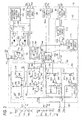
- Fig. 2 is a circuit diagram showing structures of the control circuit 10 and a periphery thereof.
- the control circuit 10 includes other members for implementing each function of the discharge lamp lighting circuit 100 in addition to members shown in Fig. 2 , the members are omitted in Fig. 2 for clarity of explanation.
- the control circuit 10 includes a temperature information converting circuit 50, a control voltage generating circuit 52, a power control circuit 54, a state detecting circuit 56, the current limiting circuit 58, an output regulating circuit 60, a polarity control circuit 62 and an output destination selecting circuit 64.
- the temperature information converting circuit 50 converts information indicative of an environment of an operation, for example, a temperature T of the discharge lamp lighting circuit 100 into the state current Is based on a predetermined converting rule.
- a dependency of the state current Is on the temperature T is used for implementing a desirable temperature characteristic through the power control circuit 54 or the current limiting circuit 58.
- the converting rule in the temperature information converting circuit 50 is set to be a rule for carrying out a conversion in such a manner that a coefficient of proportionality of the temperature T and the state current Is is varied depending on the temperature T.
- the converting rule is determined to cancel a change in the resistance value of the first ON resistor R M1 of the first switching device M1 to which the first switching current I M1 flows depending on the temperature T.
- the temperature information converting circuit 50 includes a temperature information acquiring circuit 66, a function converting circuit 68 and a GM amplifier 70.
- the temperature information acquiring circuit 66 is constituted to include a temperature sensor such as a thermal diode.
- the temperature information acquiring circuit 66 generates a detecting temperature voltage V T which is proportional to the temperature T of the discharge lamp lighting circuit 100 by using the thermal diode.
- a constant of the proportionality is determined by a measuring condition such as a current caused to flow to the thermal diode or a characteristic of the thermal diode.
- a measuring condition such as a current caused to flow to the thermal diode or a characteristic of the thermal diode.
- the function converting circuit 68 includes a first discharging type amplifying circuit 72, a second discharging type amplifying circuit 74 and a sixth resistor R6.
- the first discharging type amplifying circuit 72 outputs a temperature converting voltage Vm upon receipt of the detecting temperature voltage V T .
- the first discharging type amplifying circuit 72 includes a first differential amplifying circuit 76, a first discharging diode 78 and a plurality of resistors (not shown) for determining an amplification factor and an offset.
- the detecting temperature voltage V T is applied to a non-inverting input terminal of the first differential amplifying circuit 76.
- An anode of the first discharging diode 78 is connected to an output terminal of the first differential amplifying circuit 76.
- the temperature converting voltage Vm on a cathode side of the first discharging diode 78 is applied to an inverting input terminal of the first differential amplifying circuit 76 so that a feedback is constituted.
- the second discharging type amplifying circuit 74 has the same structure as the first discharging type amplifying circuit 72. In other words, a second differential amplifying circuit 80 and the first differential amplifying circuit 76, and a second discharging diode 82 and the first discharging diode 78 correspond to each other.
- An amplification factor and an offset which are set by the second differential amplifying circuit 80 are different from those set by the first differential amplifying circuit 76.
- One of ends of the sixth resistor R6 is connected to a third connecting node N3 to which the cathode of the first discharging diode 78 and a cathode of the second discharging diode 82 are connected. The other end of the sixth resistor R6 is grounded.
- the first discharging type amplifying circuit 72 and the second discharging type amplifying circuit 74 are connected in parallel and the detecting temperature voltage V T is input thereto.
- the temperature converting voltage Vm appearing on the third connecting node N3 to which an output of the first discharging type amplifying circuit 72 and that of the second discharging type amplifying circuit 74 are connected is a higher one of a voltage to be output by the first differential amplifying circuit 76 based on an amplification factor and offset thereof and a voltage to be output by the second differential amplifying circuit 80 based on an amplification factor and offset thereof.
- a value of the certain detecting temperature voltage V T that is, a certain threshold temperature Tth
- the temperature converting voltage Vm is thus set to be the voltage to be output by one of the discharging type amplifying circuits when the temperature T is lower than the threshold temperature Tth and the voltage to be output by the other discharging type amplifying circuit when the temperature T is equal to or higher than the threshold temperature Tth.
- the amplification factor and the offset of the first differential amplifying circuit 76 and those of the second differential amplifying circuit 80 are properly set to apply the temperature converting voltage Vm. This is expressed in the following Equation.
- the GM amplifier 70 receives the temperature converting voltage Vm and converts the temperature converting voltage Vm into the state current Is.
- An output side of the GM amplifier 70 is connected to one of ends of the fifth resistor R5 provided on the outside of the control circuit 10 through the current converting terminal P5.
- the magnitude of the state current Is generated by the GM amplifier 70 is adjusted by regulating the resistance value of the fifth resistor R5. Consequently, it is possible to finely control the magnitude of the state current Is by regulating the resistance value of the fifth resistor R5 (which is not integrated) at the outside of the control circuit 10 also after the control circuit 10 is integrated, which is convenient.
- the GM amplifier 70 includes a third differential amplifying circuit 84 and a third switching device M3.
- the temperature converting voltage Vm is applied to a non-inverting input terminal of the third differential amplifying circuit 84.
- An output terminal of the third differential amplifying circuit 84 is connected to a base of the third switching device M3 to be an npn type bipolar transistor.
- An emitter of the third switching device M3 is connected to an inverting input terminal of the third differential amplifying circuit 84 so that a feedback is formed.
- the emitter of the third switching device M3 is also connected to the current converting terminal P5.
- the control voltage generating circuit 52 generates a first reference voltage V E1 required for the power control circuit 54 and a second reference voltage V E2 required for the current limiting circuit 58 based on the state current Is.
- the control voltage generating circuit 52 regulates each of the first reference voltage V E1 and the second reference voltage V E2 by using the state current Is.
- the control voltage generating circuit 52 supplies the state current Ts to the first voltage dividing circuit 30 through the power regulating terminal P3 for the first reference voltage V E1 so that the first voltage dividing point voltage V N1 is obtained.
- the control voltage generating circuit 52 further processes the first voltage dividing point voltage V N1 into the first reference voltage V E1 .
- the control voltage generating circuit 52 supplies the state current Is to the second voltage dividing circuit 40 through the PBP regulating terminal P4 for the second reference voltage V E2 so that the second voltage dividing point voltage V N2 is obtained.
- the control voltage generating circuit 52 further processes the second voltage dividing point voltage V N2 into the second reference voltage V E2 .
- the control voltage generating circuit 52 regulates the first reference voltage V E1 in order to decrease a power to be supplied to the discharge lamp 4 when the temperature T of the discharge lamp lighting circuit 100 is higher than a predetermined temperature derating starting temperature Td.
- the temperature derating starting temperature Td is set to be higher than the threshold temperature Tth.
- the temperature derating starting temperature Td is set in such a manner that a change in the first reference voltage V E1 with respect to the temperature T is simple, particularly, linear in a temperature region in which temperature derating is required. This is preferable in respect of a control of the temperature derating function.
- the control voltage generating circuit 52 includes a current source CM and the temperature derating regulating circuit 86.
- the current source CM supplies, to the power regulating terminal P3 and the PBP regulating terminal P4, a current having the same magnitude as the state current Is generated by the GM amplifier 70.
- the current source CM is a current mirror circuit, for example.
- the current source CM includes a seventh resistor R7, an eighth resistor R8, a ninth resistor R9, a fourth switching device M4, a fifth switching device M5 and a sixth switching device M6. Resistance values of the seventh resistor R7, the eighth resistor R8 and the ninth resistor R9 are set to be equal to each other.
- All of the fourth switching device M4, the fifth switching device M5 and the sixth switching device M6 are pnp type bipolar transistors and their bases are connected in common.
- One of ends of the seventh resistor R7, one of ends of the eighth resistor R8 and one of ends of the ninth resistor R9 are connected to a source voltage Vd.
- the source voltage Vd is a separate fixed voltage from the source voltage Vcc and is 6V, for example.
- the other end of the ninth resistor R9 is connected to an emitter of the sixth switching device M6.
- a collector of the sixth switching device M6 is connected to a base of the sixth switching device M6, and furthermore, is connected to a collector of the third switching device M3.
- the other end of the eighth resistor R8 is connected to an emitter of the fifth switching device M5.
- the other end of the seventh resistor R7 is connected to an emitter of the fourth switching device M4.
- a collector of the fifth switching device M5 is connected to the power regulating terminal P3. Moreover, the collector of the fifth switching device M5 is connected to a non-inverting input terminal of a fourth differential amplifying circuit 88 of the temperature derating regulating circuit 86.
- the fifth switching device M5 supplies the state current Is from a collector thereof to the power regulating terminal P3.
- the power regulating terminal P3 is connected to the first connecting node N1 of the first voltage dividing circuit 30. Therefore, a voltage of the collector of the fifth switching device M5 is equivalent to the first voltage dividing point voltage V N1 obtained by the Equation 1. Accordingly, the first voltage dividing point voltage V N1 is applied to the non-inverting input terminal of the fourth differential amplifying circuit 88.
- a collector of the fourth switching device M4 is connected to the PBP regulating terminal P4. Moreover, the collector of the fourth switching device M4 is used as a reference voltage of the current limiting circuit 58. The fourth switching device M4 supplies the state current Is from the collector to the PBP regulating terminal P4. The PEP regulating terminal P4 is connected to the second connecting node N2 of the second voltage dividing circuit 40. Therefore, a voltage of the collector of the fourth switching device M4 is equivalent to the second voltage dividing point voltage V N2 obtained by the Equation 3.
- the temperature derating regulating circuit 86 processes the first voltage dividing point voltage V N1 to generate the first reference voltage V E1 .
- the temperature derating regulating circuit 86 regulates the first reference voltage V E1 in order to decrease a power to be supplied to the discharge lamp 4 when the temperature T of the discharge lamp lighting circuit 100 is higher than the temperature derating starting temperature Td.
- the temperature derating regulating circuit 86 includes the fourth differential amplifying circuit 88, a seventh switching device M7, a tenth resistor R10, an eleventh resistor R11, a twelfth resistor R12, a thirteenth resistor R13, and a fourteenth resistor R14.
- An output terminal of the fourth differential amplifying circuit 88 is connected to a base of the seventh switching device M7 to be an npn type bipolar transistor.
- the tenth resistor R10, the eleventh resistor R11 and the twelfth resistor R12 are provided in this order in series between the power terminal (Vcc) and the grounding terminal.
- a voltage of a fourth connecting node N4 between one of ends of the tenth resistor R10 and one of ends of the eleventh resistor R11 is applied to an inverting input terminal of the fourth differential amplifying circuit 88.
- a fifth connecting node N5 between the other end of the eleventh resistor R11 and one of ends of the twelfth resistor R12 is connected to an emitter of the seventh switching device M7.
- the thirteenth resistor R13 and the fourteenth resistor R14 are provided in this order in series between the power terminal (Vcc) and the grounding terminal.
- a sixth connecting node N6 between one of ends of the thirteenth resistor R13 and one of ends of the fourteenth resistor R14 is connected to a collector of the seventh switching device M7.
- a voltage of the sixth connecting node N6 is supplied as the first reference voltage V E1 to the power control circuit 54.
- a sink current Io is started to be led from the sixth connecting node N6 when the first voltage dividing point voltage V N1 reaches a certain threshold voltage Vth.
- Equation 1 R ⁇ 1 ⁇ R ⁇ 2 R ⁇ 1 + R ⁇ 2 ⁇ V m R ⁇ 5 + R ⁇ 2 R ⁇ 1 + R ⁇ 2 ⁇ V CC
- Substitute Equation 6 R ⁇ 1 ⁇ R ⁇ 2 R ⁇ 1 + R ⁇ 2 ⁇ R ⁇ 5 ⁇ A ⁇ 2 ⁇ T + B ⁇ 2 + R ⁇ 2 R ⁇ 1 + R ⁇ 2 ⁇ V CC
- Equation 6 R ⁇ 1 ⁇ R ⁇ 2 R ⁇ 1 + R ⁇ 2 ⁇ R ⁇ 5 ⁇ A ⁇ 2 ⁇ T + B ⁇ 2 + R ⁇ 2 R ⁇ 1 + R ⁇ 2 ⁇ V CC
- T > Td > Tth was used.
- the first reference voltage V E1 is obtained by using the sink current Io through the following Equation 10.
- V E ⁇ 1 R ⁇ 13 ⁇ R ⁇ 14 R ⁇ 13 + R ⁇ 14 ⁇ V CC R ⁇ 13 - I O
- the sink current Io is increased with a rise in the temperature T so that the first reference voltage V E1 reaches zero, the first reference voltage V E1 is zero or has a predetermined small value even if the temperature T is raised more greatly.
- the second amplification factor A2, the second offset B2, the source voltage Vcc and the resistance value of the twelfth resistor R12 are given and a characteristic of desirable temperature derating, that is, a tilt of the sink current Io to the temperature T at the temperature derating starting temperature Td within a temperature range of T > Td is given, it is possible to determine a ratio among the first resistor R1, the second resistor R2 and the fifth resistor R5 by using the Equations 8 and 9.
- the characteristic of the desirable temperature derating by regulating the resistance values of the first resistor R1 the second resistor R2 and the fifth resistor R5 also after the control circuit 10 is integrated. This is useful when a variation in the characteristic of each electronic component to be used for the discharge lamp lighting circuit 100 is corrected or the derating characteristic is adjusted based on a difference in a temperature environment in which the discharge lamp lighting circuit 100 is provided, for example.
- the state detecting circuit 56 detects an electrical state of the discharge lamp 4 upon receipt of the current detection signal S IL , the first output voltage Vo1 and the second output voltage Vo2.
- the state detecting circuit 56 outputs, to the power control circuit 54, a power information signal Sp indicative of the electrical state of the discharge lamp 4, for example, a driving power (VL X IL).
- the power control circuit 54 receives the first reference voltage V E1 as a voltage indicative of a target state.
- the power control circuit 54 generates an error signal Serr corresponding to a difference between the first reference voltage V E1 and a voltage of the power information signal Sp.
- the power control circuit 54 includes an error amplifier 90 and a phase compensating circuit 92.
- the error amplifier 90 amplifies an error between the first reference voltage V E1 and the voltage of the power information signal Sp and generates the error signal Serr.
- the phase compensating circuit 92 compensates a phase of the error signal Serr for that of the power information signal Sp and prevents an oscillation of the whole control circuit 10.
- the phase compensating circuit 92 includes a phase compensating capacitor C2 and a fifteenth resistor R15 which are provided in parallel between the power information signal Sp and the error signal Serr.
- the polarity control circuit 62 generates an inverter signal S INV and supplies the inverter signal S INV to a switch control circuit 102 and the output destination selecting circuit 64.
- the inverter signal S INV takes complementary levels in the first state ⁇ 1 and the second state ⁇ 2.
- the inverter signal S INV is set to have a high level in the first state ⁇ 1 and to have a low level in the second state ⁇ 2.
- the polarity control circuit 62 generates the first control signal S3 and the second control signal S4 based on whether the discharge lamp lighting circuit 100 is set in the first state ⁇ 1 or the second state ⁇ 2.
- the output regulating circuit 60 controls a duty ratio of ON/OFF of the switching device in each of the DC/DC converters based on the error signal Serr.
- the output regulating circuit 60 includes a PWM comparator 108, a sawtooth generating circuit 110 and a duty ratio limiting circuit 112.
- the sawtooth generating circuit 110 generates a triangular wave-shaped or sawtooth cyclic signal Sosc having a PWM frequency f2.
- the PWM comparator 108 compares the error signal Serr with the cyclic signal Sosc, thereby generating a prelimitation PWM signal S8.
- the duty ratio limiting circuit 112 receives the prelimitation PWM signal S8 and a PBP regulating signal S7 which will be described below.
- the duty ratio limiting circuit 112 generates a PWM signal S PWM having a waveform aligned with the prelimitation PWM signal S8 except for the following case.
- the duty ratio limiting circuit 112 sets the PWM signal S PWM into a low level when the PBP regulating signal S7 is set to have the low level for a period for which the prelimitation PWM signal S8 has a high level.
- the duty ratio limiting circuit 112 sets the PWM signal S PWM to have the high level in a timing in which the prelimitation PWM signal S8 is then set to have the high level.
- the output destination selecting circuit 64 receives the inverter signal S INV and the PWM signal S PWM .
- the output destination selecting circuit 64 is constituted to include a buffer circuit for amplifying the PWM signal S PWM .
- the output destination selecting circuit 64 outputs the amplified PWM signal S PWM as the first control pulse signal S1 to a control terminal of the first switching device M1 when the inverter signal S INV takes a high level. In this case, the output destination selecting circuit 64 fixes the second control pulse signal S2 into a low level, thereby turning OFF the second switching device M2.
- the output destination selecting circuit 64 outputs the amplified PWM signal S PWM as the second control pulse signal S2 to a control terminal of the second switching device M2 when the inverter signal S INV takes the low level. In this case, the output destination selecting circuit 64 fixes the first control pulse signal S1 into the low level, thereby turning OFF the first switching device M1.
- the current limiting circuit 58 carries out a control for limiting the switching current flowing to the switching device in each of the DC/DC converters.
- the second voltage dividing point voltage V N2 can be regulated by the resistance values of the third resistor R3 and the fourth resistor R4. in other words, also after the control circuit 10 is integrated, it is possible to set the maximum current I M_MAX to be a desirable current value by regulating the resistance values of the third resistor R3 and the fourth resistor R4. This is useful in an execution of a correction depending on absolute values of ON resistances of the first and second switching devices M1 and M2 used in the discharge lamp lighting circuit 100 or temperature characteristics thereof, for example.
- the current limiting circuit 58 includes the first PBP monitoring circuit 94, the second PBP monitoring circuit 96, an AND gate 98 and a switch control circuit 102.
- the switch control circuit 102 controls ON/OFF of a third switch SW3 and a fourth switch SW4 upon receipt of the inverter signal S INV and the PWM signal S PWM from the polarity control circuit 62 and the duty ratio limiting circuit 112, respectively.
- the first PBP monitoring circuit 94 includes a first PBP comparator 104, an eighth switching device M8, the third switch SW3, a sixteenth resistor R16 and a seventeenth resistor R17.
- the first drain voltage V M1 is applied to one of ends of the sixteenth resistor R16.
- the other end of the sixteenth resistor R16 is connected to one of ends of the third switch SW3 and a non-inverting input terminal of the first PBP comparator 104.
- the other end of the third switch SW3 is grounded. ON/OFF of the third switch SW3 is controlled by the switch control circuit 102.
- the switch control circuit 102 turns OFF the third switch SW3 when the PWM signal S PWM has the high level, that is, the first switching device M1 is ON, and turns ON the third switch SW3 when the PWM signal S PWM has the low level, that is, the first switching device M1 is OFF.
- the switch control circuit 102 turns ON the third switch SW3 in the second state ⁇ 2. In other words, the switch control circuit 102 turns OFF the third switch SW3 when the first switching device M1 is ON, and turns ON the third switch SW3 when the first switching device M1 is OFF.
- the second reference voltage V E2 is applied to an inverting input terminal of the first PBP comparator 104.
- the seventeenth resistor R17 and the eighth switching device M8 are provided in series in this order between a power terminal to which the source voltage Vcc is applied and a grounding terminal.
- the eighth switching device M8 is constituted by an N-channel MOSFET.
- An output terminal of the first PBP comparator 104 is connected to a gate of the eighth switching device M8.
- a first PBP regulating signal S5 generated on a node of one of ends of the seventeenth resistor R17 and a drain of the eighth switching device M8 is supplied to the AND gate 98.
- the eighth switching device M8 is turned ON so that the first PBP regulating signal S5 is set to have the low level.
- the first switching device M1 is turned OFF until an ON period corresponding to a residual one pulse is ended after the first PBP regulating signal S5 is set to have the low level in the duty ratio limiting circuit 112. Since the first switching device M1 is turned OFF, the third switch SN3 is turned ON so that the eighth switching device M8 is turned OFF again.
- the second PBP monitoring circuit 96 has the same structure as the first PBP monitoring circuit 94. More specifically, a second PBP comparator 106 and the first PBP comparator 104, a ninth switching device M9 and the eighth switching device M8, the fourth switch SW4 and the third switch SW3, an eighteenth resistor R18 and the sixteenth resistor R16, and a nineteenth resistor R19 and the seventeenth resistor R17 correspond to each other.
- the second drain voltage V M2 is applied to one of ends of the eighteenth resistor R18.
- the switch control circuit 102 turns OFF the fourth switch SW4 when the PWM signal S PWM has the high level, that is, the second switching device M2 is ON, and turns ON the fourth switch SW4 when the PWM signal S PWM has the low level, that is, the second switching device M2 is OFF.
- the switch control circuit 102 turns ON the fourth switch SW4 in the first state ⁇ 1. In other words, the switch control circuit 102 turns OFF the fourth switch SW4 when the second switching device M2 is ON, and turns ON the fourth switch SW4 when the second switching device M2 is OFF.
- the ninth switching device M9 is turned ON so that a second PBP regulating signal S6 is set to have the low level.
- the second switching device M2 is turned OFF until an ON period corresponding to a residual one pulse is ended after the second PBP regulating signal S6 is set to have the low level in the duty ratio limiting circuit 112. Since the second switching device M2 is turned OFF, the fourth switch SW4 is turned ON so that the ninth switching device M9 is turned OFF again.
- the AND gate 98 outputs, to the duty ratio limiting circuit 112, AND of the first PBP regulating signal S5 and the second PBP regulating signal S6 as a PBP regulating signal S7.
- Fig. 3 is a time chart showing a waveform related to the current limiting function of the control circuit 10.
- An axis of ordinate and an axis of abscissa in Fig. 3 are properly enlarged and reduced for easy understanding, and each waveform shown in Fig. 3 is also simplified for the easy understanding.
- the cyclic signal Sosc, the prelimitation PWM signal S8, the PBP regulating signal S7 and the PWM signal S PWM are shown from an upper part.
- a broken line shown in the same column as the cyclic signal Sosc indicates a voltage Verr of the error signal Serr.
- the first drain voltage V M1 exceeds the second reference voltage V E2 for the ON period of the first switching device M1 in the first state ⁇ 1.
- the eighth switching device M8 is turned ON by the first PBP comparator 104 so that the PBP regulating signal S7 is set to have the low level.
- the duty ratio limiting circuit 112 sets the PWM signal S PWM to have the low level at the time t1 upon receipt of the fact that the PBP regulating signal S7 is set to have the low level. Since the first switching device M1 is turned OFF, the third switch SW3 is turned ON and the eighth switching device M8 is turned OFF again, and the PBP regulating signal S7 is returned to have the high level.
- a time required for the PBP regulating signal S7 to be once set into the low level and to be then returned into the high level is much shorter than a time scale shown in Fig. 3 .
- the PBP regulating signal S7 is drawn as a signal having a pulse dropped into the low level at the time t1.
- the PWM signal S PWM is also set to have the high level at a time t2 that a leading edge appears in the prelimitation PWM signal S8.
- the ON period of the first switching device M1 is also limited for each pulse as long as there is continuously maintained a state in which an amount of the first switching current I M1 flowing to the first switching device M1 is larger than that of the maximum current I M_MAX defined by the second reference voltage V E2 . Consequently, it is possible to prevent an overcurrent from flowing to the first switching device M1.
- the second switching device M2 is also the same.
- Fig. 4 is a graph showing an example of the converting rule in the temperature information converting circuit 50. Since the first ON resistance R M1 and the second ON resistance R M2 have the same absolute values and temperature characteristics, they are generally represented as an ON resistance R M .
- a curve 114 represents (the ON resistance R M ). (the maximum current I M_MAX ). The curve 114 indicates a curved change in a temperature of the ON resistance R M .
- the first segment 116 and the second segment 118 correspond to Equations 11 and 12, respectively.
- the first amplification factor A1, the second amplification factor A2, the first offset B1 and the second offset B2 (which are the converting rules in the temperature information converting circuit 50), and resistance values of the third resistor R3, the fourth resistor R4 and the fifth resistor R5 are determined in such a manner that the first segment 116 and the second segment 118 approximate to the curve 114 greatly.
- Fig. 5 is a time chart showing an operating state of the discharge lamp lighting circuit 100.
- An axis of ordinate and an axis of abscissa in Fig. 5 are properly enlarged and reduced for easy understanding, and each waveform shown in Fig. 5 is simplified for the easy understanding.
- the control circuit 10 sets the first DC/DC converter CONV1 into the active state and sets the first switch SW1 into an OFF state (the first state ⁇ 1), and raises the battery voltage Vbat into a predetermined high voltage (400V), thereby carrying out a stabilization.
- the starter circuit 20 receives the first output voltage Vo1 of 400V which is generated by the first DC/DC converter CONV1.
- the pulse generating portion 28 applies a pulse having an amplitude of 400V to the primary coil 24 of the starter transformer 22.
- a high voltage pulse of 20 kV or more is generated in the secondary coil 26 of the starter transformer 22 at this time.
- the driving voltage of the discharge lamp 4 is raised to approximately 13 to 25 kV and breaks down at the time t2 so that a glow discharge is started.
- the control circuit 10 After the breakdown, first of all, the control circuit 10 carries out a control for causing the lamp current IL to flow for approximately 10 ms in a direction of the first polarity in the first state ⁇ 1. Next, the control circuit 10 carries out switching into the second state ⁇ 2 and performs a control for causing the lamp current IL to flow for approximately 10 ms in a direction of the second polarity.
- the period will be referred to as a DC period ⁇ DC .
- a transition from the glow discharge to an arc discharge is made.
- the control circuit 10 controls the first DC/DC converter CONV1, the second DC/DC converter CONV2, the first switch SW1 and the second switch SW2 to alternately repeat the first state ⁇ 1 and the second state ⁇ 2 in the lighting cycle T1.
- Figs. 6A and 6B are time charts showing an operating state after the DC period ⁇ DC of the discharge lamp lighting circuit 100.
- An axis of ordinate and an axis of abscissa in each of Figs. 6A and 6B are properly enlarged and reduced for easy understanding.
- each waveform shown in Figs. 6A and 6B is also simplified for the easy understanding.
- Figs. 6A and 6B show a waveform in a run-up process and stationary lighting, respectively.
- a light output of the discharge lamp 4 is raised.
- a rise in the light output is determined by the standards, and the control circuit 10 monitors the first output voltage Vo1, the second output voltage Vo2 and the lamp current IL and regulates a duty ratio of ON/OFF operations of the first switching device M1 and the second switching device M2 through a feedback in order to obtain a light output (power) matched with the standards.
- the discharge lamp lighting circuit 100 temporarily supplies a higher overpower than a rated power and then stabilizes the lamp voltage and the lamp current IL to be 45V and 0.8A respectively, thereby approximating to the rated power (35W) in order to rapidly raise the light output of the discharge lamp 4 for a run-up period ( Fig. 6A ).
- the power to be supplied to the discharge lamp 4 is stabilized to have the rated value of 35W ( Fig. 6B ).
- the waveforms of the driving voltage VL and the lamp current IL shown in Figs. 6A and 6B are simplified to be easily seen, and actually have frequencies of 250 Hz to 750 Hz.
- the current limiting function and the temperature derating function described with reference to Figs. 1 to 4 are operated in the stationary lighting state, moreover, it is a matter of course that they may be operated in another state (until the stationary lighting state is brought after the ON operation).
- the operation of the discharge lamp lighting circuit 100 according to the embodiment has been described above.
- the discharge lamp lighting circuit 100 has the following advantages.
- the temperature T of the discharge lamp lighting circuit 100 is converted into the state current Is by only one temperature information converting circuit 50.
- the state current Is is caused to act on the reference voltage to be used in each of the temperature derating function and the current limiting function, thereby transferring information about the temperature T to each of the functions.
- the temperature information converting circuit 50 is shared by the temperature derating function and the current limiting function.
- the temperature characteristic of the reference voltage required for the current limiting function (for example, the curve 114 in Fig. 4 ) is different from the temperature characteristic of the reference voltage required for the temperature derating function (for example, the sink current Io in the Equation 8).
- the respective temperature characteristics are implemented by properly setting the resistance values of the first resistor R1, the second resistor R2, the third resistor R3, the fourth resistor R4 and the fifth resistor R5.
- the state current Is is not processed in the portion in which the control circuit 10 is integrated for each temperature characteristic but the state current Is is maintained as it is and the resistance values of the resistors provided on the outside of the integrated portion are regulated to implement the respective temperature characteristics.
- the converting rule in the temperature information converting circuit 50 is set to be a rule for converting the coefficient of proportionality of the temperature T and the state current Is to be varied depending on the temperature T. Consequently, it is also possible to correspond to a complicated temperature characteristic such as a nonlinear temperature characteristic. Moreover, the converting rule is determined to cancel a change in the resistance value of the first ON resistor R M1 of the first switching device M1 to which the first switching current I M1 flows depending on the temperature T. As seen in Fig. 4 , therefore, the threshold current of the switching current is maintained to be almost equal to the maximum current I M_MAX even if the ON resistance R M is varied depending on the temperature T. In other words, the threshold current can be set to be almost constant without depending on the temperature T.
- the discharge lamp lighting circuit 100 Since the discharge lamp lighting circuit 100 according to the embodiment is mounted on a lighting device for a vehicle, moreover, a comparatively high temperature is obtained. In the situation, the discharge lamp lighting circuit 100 has the temperature derating function and the current limiting function in which a change depending on a temperature is compensated. Therefore, a safety of the discharge lamp lighting circuit 100 is higher than that of the related-art discharge lamp lighting circuit.
- Fig. 7 is a circuit diagram showing a structure of a temperature derating regulating circuit 120 according to the variant.
- the temperature derating regulating circuit 120 includes a twentieth resistor R20, a fifth differential amplifying circuit 122, a first voltage source 124, a tenth switching device M10, an eleventh switching device M11, a twelfth switching device M12, a thirteenth switching device M13, a thirteenth resistor R13, and a fourteenth resistor R14.
- the first voltage dividing point voltage V N1 is applied to one of ends of the twentieth resistor R20.
- the other end of the twentieth resistor R20 is connected to an emitter of the tenth switching device M10 to be a pnp type bipolar transistor and an inverting input terminal of the fifth differential amplifying circuit 122.
- a third reference voltage V E3 is applied from the first voltage source 124 to a non-inverting input terminal of the fifth differential amplifying circuit 122.
- An output terminal of the fifth differential amplifying circuit 122 is connected to a base of the tenth switching device M10.
- a collector of the tenth switching device M10 is connected to a collector of the twelfth switching device M12 to be an npn type bipolar transistor and a base of the eleventh switching device M11 to be the npn type bipolar transistor.
- a base of the twelfth switching device M12 is connected to a base of the thirteenth switching device M13 to be the npn type bipolar transistor in common.
- An emitter of the twelfth switching device M12 is connected to an emitter of the thirteenth switching device M13 and is grounded.
- a source voltage Vcc is applied to a collector of the eleventh switching device M11.
- An emitter of the eleventh switching device M11 is connected to the base of the twelfth switching device M12.
- a collector of the thirteenth switching device M13 is connected to a sixth connecting node N6' of the thirteenth resistor R13 and the fourteenth resistor R14.
- a voltage of the sixth connecting node N6' is supplied as a first reference voltage V E1 ' to an error amplifier 90.
- a sink current Io' is started to flow.
- the first reference voltage V E1 ' of the sixth connecting node N6' is dropped.
- the sink current Io' is increased corresponding to the drop in the first reference voltage V E1 '. Consequently, a temperature derating function can be implemented.
- the regulation based on the derating information is not carried out over the power information signal Sp side (the control line side) of the error amplifier 90 but the regulation based on the derating information is carried out over the reference voltage side of the error amplifier 90.
- FIG. 8 is a circuit diagram showing a structure of a battery voltage derating regulating circuit 126 in relation to the derating function of a battery voltage Vbat.
- the battery voltage derating regulating circuit 126 supplies a first reference voltage VE1" to a non-inverting input terminal of the error amplifier 90 in place of the temperature derating regulating circuit 86.
- the battery voltage derating regulating circuit 126 includes a fourteenth switching device M14, a fifteenth switching device M15, a sixteenth switching device M16, a seventeenth switching device M17, an eighteenth switching device M18, a nineteenth switching device M19, a twentieth switching device M20, a sixth differential amplifying circuit 128, a buffer 130, a second voltage source 132, a twenty-first resistor R21, a thirteenth resistor R13, and a fourteenth resistor R14.
- the source voltage Vcc is applied to an emitter of the fourteenth switching device M14 to be a pnp type bipolar transistor and an emitter of the fifteenth switching device M15 to be the pnp type bipolar transistor.
- the fourteenth switching device M14 and the fifteenth switching device M15 have bases connected in common, and the bases are connected to an emitter of the sixteenth switching device M16 to be the pnp type bipolar transistor.
- the sixteenth switching device M16 has a collector grounded and has a base connected to a collector of the fourteenth switching device M14.
- the collector of the fourteenth switching device M14 is connected to a drain of the seventeenth switching device M17 to be an N-channel MOSFET.
- a fourth reference voltage V E4 is applied from the second voltage source 132 to a non-inverting input terminal of the sixth differential amplifying circuit 128.
- the sixth differential amplifying circuit 128 has an output terminal connected to a gate of the seventeenth switching device M17 and has an inverting input terminal connected to a source of the seventeenth switching device M17.
- the source of the seventeenth switching device M17 is connected to one of ends of the twenty-first resistor R21.
- a voltage which is equivalent to the battery voltage Vbat (which will be hereinafter referred to as a battery equivalent voltage Vbat') is buffered by the buffer 130 and is thus applied to the other end of the twenty-first resistor R21.
- the fifteenth switching device M15 has a collector connected to a base of the twentieth switching device M20 to be an npn type bipolar transistor and a collector of the eighteenth switching device M18 to be the npn type bipolar transistor.
- a base of the eighteenth switching device M18 is connected to a base of the nineteenth switching device M19 to be the npn type bipolar transistor, and furthermore, is also connected to an emitter of the twentieth switching device M20.
- An emitter of the eighteenth switching device M18 and that of the nineteenth switching device M19 are grounded together.
- the source voltage Vcc is applied to a collector of the twentieth switching device M20.
- the nineteenth switching device M19 has a collector connected to a sixth connecting node N6" of the thirteenth resistor R13 and the fourteenth resistor R14.
- a sink current Io is started to flow to the nineteenth switching device M19.
- the first reference voltage V E1 " of the sixth connecting node N6" is dropped.
- the sink current Io is increased corresponding to the drop in the first reference voltage V E1 ". Consequently, the derating function of the battery voltage Vbat can be implemented.
- the temperature derating function may be regulated by sourcing a current or the temperature derating function may be regulated by a combination of the sink and source of the current.
- the discharge lamp lighting circuit 100 for driving the discharge lamp 4 for a vehicle the use of the invention is not restricted thereto.
- the invention can be widely applied to a lighting circuit of a light source such as an LED with a lamp current to be a direct current to which the operating sequence cannot be applied, particularly, a light source lighting circuit for carrying out a control based on information indicative of an environment of an operation.
- the logical values of the high and low levels of the signal are set as illustrative in the circuit described in the embodiment, and can be freely changed through a proper inversion by means of an inverter.
Landscapes
- Circuit Arrangements For Discharge Lamps (AREA)
Applications Claiming Priority (1)
| Application Number | Priority Date | Filing Date | Title |
|---|---|---|---|
| JP2009107087A JP5280290B2 (ja) | 2009-04-24 | 2009-04-24 | 光源点灯回路 |
Publications (3)
| Publication Number | Publication Date |
|---|---|
| EP2244537A2 true EP2244537A2 (fr) | 2010-10-27 |
| EP2244537A3 EP2244537A3 (fr) | 2013-04-10 |
| EP2244537B1 EP2244537B1 (fr) | 2017-12-27 |
Family
ID=42341392
Family Applications (1)
| Application Number | Title | Priority Date | Filing Date |
|---|---|---|---|
| EP10160867.7A Not-in-force EP2244537B1 (fr) | 2009-04-24 | 2010-04-23 | Circuit d'éclairage à source lumineuse |
Country Status (2)
| Country | Link |
|---|---|
| EP (1) | EP2244537B1 (fr) |
| JP (1) | JP5280290B2 (fr) |
Cited By (3)
| Publication number | Priority date | Publication date | Assignee | Title |
|---|---|---|---|---|
| WO2012120435A3 (fr) * | 2011-03-10 | 2012-11-08 | Koninklijke Philips Electronics N.V. | Procédé permettant d'exciter une lampe à décharge de gaz |
| WO2015155156A3 (fr) * | 2014-04-07 | 2015-12-10 | Koninklijke Philips N.V. | Agencement d'allumage |
| CN111955055A (zh) * | 2018-04-10 | 2020-11-17 | 株式会社小糸制作所 | 车辆用灯具及其点亮电路、驱动电路、驱动一体化光源 |
Citations (1)
| Publication number | Priority date | Publication date | Assignee | Title |
|---|---|---|---|---|
| JPH11329777A (ja) | 1998-05-08 | 1999-11-30 | Denso Corp | 放電灯装置 |
Family Cites Families (7)
| Publication number | Priority date | Publication date | Assignee | Title |
|---|---|---|---|---|
| US4677346A (en) * | 1985-10-28 | 1987-06-30 | General Electric Company | Drive and control circuits for gate capacitance latch with refresh lamp ballast |
| US6259215B1 (en) * | 1998-08-20 | 2001-07-10 | Romlight International, Inc. | Electronic high intensity discharge ballast |
| JP3942387B2 (ja) * | 2001-02-13 | 2007-07-11 | 株式会社小糸製作所 | 放電灯点灯回路 |
| JP4308453B2 (ja) * | 2001-07-16 | 2009-08-05 | パナソニック電工株式会社 | 放電灯点灯装置 |
| US7183727B2 (en) * | 2003-09-23 | 2007-02-27 | Microsemi Corporation | Optical and temperature feedbacks to control display brightness |
| US6982528B2 (en) * | 2003-11-12 | 2006-01-03 | Lutron Electronics Co., Inc. | Thermal protection for lamp ballasts |
| US7294979B2 (en) * | 2005-05-27 | 2007-11-13 | Hewlett-Packard Development Company, L.P. | Light source module with temperature sensor |
-
2009
- 2009-04-24 JP JP2009107087A patent/JP5280290B2/ja not_active Expired - Fee Related
-
2010
- 2010-04-23 EP EP10160867.7A patent/EP2244537B1/fr not_active Not-in-force
Patent Citations (1)
| Publication number | Priority date | Publication date | Assignee | Title |
|---|---|---|---|---|
| JPH11329777A (ja) | 1998-05-08 | 1999-11-30 | Denso Corp | 放電灯装置 |
Cited By (8)
| Publication number | Priority date | Publication date | Assignee | Title |
|---|---|---|---|---|
| WO2012120435A3 (fr) * | 2011-03-10 | 2012-11-08 | Koninklijke Philips Electronics N.V. | Procédé permettant d'exciter une lampe à décharge de gaz |
| US9161423B2 (en) | 2011-03-10 | 2015-10-13 | Koninklijke Philips N.V. | Method of driving a gas-discharge lamp |
| WO2015155156A3 (fr) * | 2014-04-07 | 2015-12-10 | Koninklijke Philips N.V. | Agencement d'allumage |
| US10070506B2 (en) | 2014-04-07 | 2018-09-04 | Lumileds Llc | Ignitor-arrangement |
| CN111955055A (zh) * | 2018-04-10 | 2020-11-17 | 株式会社小糸制作所 | 车辆用灯具及其点亮电路、驱动电路、驱动一体化光源 |
| CN111955055B (zh) * | 2018-04-10 | 2023-02-28 | 株式会社小糸制作所 | 车辆用灯具及其点亮电路 |
| US11602029B2 (en) | 2018-04-10 | 2023-03-07 | Koito Manufacturing Co., Ltd. | Automotive lamp |
| US11612034B2 (en) | 2018-04-10 | 2023-03-21 | Koito Manufacturing Co., Ltd. | Automotive lamp |
Also Published As
| Publication number | Publication date |
|---|---|
| JP2010257795A (ja) | 2010-11-11 |
| EP2244537A3 (fr) | 2013-04-10 |
| EP2244537B1 (fr) | 2017-12-27 |
| JP5280290B2 (ja) | 2013-09-04 |
Similar Documents
| Publication | Publication Date | Title |
|---|---|---|
| US7729137B2 (en) | Switching power supply and regulation circuit | |
| JP4675319B2 (ja) | 直流−交流変換装置、そのコントローラic、及びその直流−交流変換装置を用いた電子機器 | |
| KR100983703B1 (ko) | 직류-교류 변환 장치 및 교류 전력 공급 방법 | |
| US7426125B2 (en) | Adjustable compact high-frequency-high-voltage power supply | |
| JP6476997B2 (ja) | 電源制御用半導体装置 | |
| US7414371B1 (en) | Voltage regulation loop with variable gain control for inverter circuit | |
| US20120313433A1 (en) | Switching power supply apparatus | |
| JP5229495B2 (ja) | スイッチング装置及びその制御方法 | |
| JP2000268990A (ja) | 放電灯点灯回路 | |
| US20170077825A1 (en) | Switching power supply device | |
| JP2009038218A (ja) | 発光ダイオード駆動回路 | |
| KR20050073536A (ko) | 직류-교류 변환 장치 및 그 제어 회로 ic | |
| US7075806B2 (en) | DC voltage conversion circuit | |
| US7006363B2 (en) | DC-DC converter circuit having correction circuit for outputting voltage level inversely proportional to input voltage | |
| US6853170B2 (en) | DC-DC converter and DC-DC converter drive circuit | |
| EP2244537B1 (fr) | Circuit d'éclairage à source lumineuse | |
| JP2019205218A (ja) | 電力変換回路 | |
| US20030198066A1 (en) | Switching power supply | |
| JP5834596B2 (ja) | 高電圧インバータ装置 | |
| JP2019080433A (ja) | 同期整流回路及びスイッチング電源装置 | |
| JP2010198860A (ja) | 放電灯点灯回路 | |
| JP2002231480A (ja) | 放電灯点灯回路 | |
| US8063569B2 (en) | Discharge tube power supply apparatus and semiconductor integrated circuit | |
| US8184416B2 (en) | Inverter driver and lamp driver thereof | |
| JP2003164163A (ja) | 圧電トランス駆動回路 |
Legal Events
| Date | Code | Title | Description |
|---|---|---|---|
| PUAI | Public reference made under article 153(3) epc to a published international application that has entered the european phase |
Free format text: ORIGINAL CODE: 0009012 |
|
| 17P | Request for examination filed |
Effective date: 20100423 |
|
| AK | Designated contracting states |
Kind code of ref document: A2 Designated state(s): AT BE BG CH CY CZ DE DK EE ES FI FR GB GR HR HU IE IS IT LI LT LU LV MC MK MT NL NO PL PT RO SE SI SK SM TR |
|
| AX | Request for extension of the european patent |
Extension state: AL BA ME RS |
|
| PUAL | Search report despatched |
Free format text: ORIGINAL CODE: 0009013 |
|
| AK | Designated contracting states |
Kind code of ref document: A3 Designated state(s): AT BE BG CH CY CZ DE DK EE ES FI FR GB GR HR HU IE IS IT LI LT LU LV MC MK MT NL NO PL PT RO SE SI SK SM TR |
|
| AX | Request for extension of the european patent |
Extension state: AL BA ME RS |
|
| RIC1 | Information provided on ipc code assigned before grant |
Ipc: H05B 41/292 20060101AFI20130305BHEP |
|
| 17Q | First examination report despatched |
Effective date: 20140115 |
|
| GRAP | Despatch of communication of intention to grant a patent |
Free format text: ORIGINAL CODE: EPIDOSNIGR1 |
|
| STAA | Information on the status of an ep patent application or granted ep patent |
Free format text: STATUS: GRANT OF PATENT IS INTENDED |
|
| INTG | Intention to grant announced |
Effective date: 20170919 |
|
| GRAS | Grant fee paid |
Free format text: ORIGINAL CODE: EPIDOSNIGR3 |
|
| GRAA | (expected) grant |
Free format text: ORIGINAL CODE: 0009210 |
|
| STAA | Information on the status of an ep patent application or granted ep patent |
Free format text: STATUS: THE PATENT HAS BEEN GRANTED |
|
| AK | Designated contracting states |
Kind code of ref document: B1 Designated state(s): AT BE BG CH CY CZ DE DK EE ES FI FR GB GR HR HU IE IS IT LI LT LU LV MC MK MT NL NO PL PT RO SE SI SK SM TR |
|
| REG | Reference to a national code |
Ref country code: GB Ref legal event code: FG4D |
|
| REG | Reference to a national code |
Ref country code: CH Ref legal event code: EP |
|
| REG | Reference to a national code |
Ref country code: AT Ref legal event code: REF Ref document number: 959374 Country of ref document: AT Kind code of ref document: T Effective date: 20180115 |
|
| REG | Reference to a national code |
Ref country code: IE Ref legal event code: FG4D |
|
| REG | Reference to a national code |
Ref country code: DE Ref legal event code: R096 Ref document number: 602010047604 Country of ref document: DE |
|
| PG25 | Lapsed in a contracting state [announced via postgrant information from national office to epo] |
Ref country code: LT Free format text: LAPSE BECAUSE OF FAILURE TO SUBMIT A TRANSLATION OF THE DESCRIPTION OR TO PAY THE FEE WITHIN THE PRESCRIBED TIME-LIMIT Effective date: 20171227 Ref country code: FI Free format text: LAPSE BECAUSE OF FAILURE TO SUBMIT A TRANSLATION OF THE DESCRIPTION OR TO PAY THE FEE WITHIN THE PRESCRIBED TIME-LIMIT Effective date: 20171227 Ref country code: NO Free format text: LAPSE BECAUSE OF FAILURE TO SUBMIT A TRANSLATION OF THE DESCRIPTION OR TO PAY THE FEE WITHIN THE PRESCRIBED TIME-LIMIT Effective date: 20180327 |
|
| REG | Reference to a national code |
Ref country code: NL Ref legal event code: MP Effective date: 20171227 |
|
| REG | Reference to a national code |
Ref country code: LT Ref legal event code: MG4D |
|
| REG | Reference to a national code |
Ref country code: AT Ref legal event code: MK05 Ref document number: 959374 Country of ref document: AT Kind code of ref document: T Effective date: 20171227 |
|
| PG25 | Lapsed in a contracting state [announced via postgrant information from national office to epo] |
Ref country code: HR Free format text: LAPSE BECAUSE OF FAILURE TO SUBMIT A TRANSLATION OF THE DESCRIPTION OR TO PAY THE FEE WITHIN THE PRESCRIBED TIME-LIMIT Effective date: 20171227 Ref country code: BG Free format text: LAPSE BECAUSE OF FAILURE TO SUBMIT A TRANSLATION OF THE DESCRIPTION OR TO PAY THE FEE WITHIN THE PRESCRIBED TIME-LIMIT Effective date: 20180327 Ref country code: LV Free format text: LAPSE BECAUSE OF FAILURE TO SUBMIT A TRANSLATION OF THE DESCRIPTION OR TO PAY THE FEE WITHIN THE PRESCRIBED TIME-LIMIT Effective date: 20171227 Ref country code: GR Free format text: LAPSE BECAUSE OF FAILURE TO SUBMIT A TRANSLATION OF THE DESCRIPTION OR TO PAY THE FEE WITHIN THE PRESCRIBED TIME-LIMIT Effective date: 20180328 |
|
| PG25 | Lapsed in a contracting state [announced via postgrant information from national office to epo] |
Ref country code: NL Free format text: LAPSE BECAUSE OF FAILURE TO SUBMIT A TRANSLATION OF THE DESCRIPTION OR TO PAY THE FEE WITHIN THE PRESCRIBED TIME-LIMIT Effective date: 20171227 |
|
| PG25 | Lapsed in a contracting state [announced via postgrant information from national office to epo] |
Ref country code: EE Free format text: LAPSE BECAUSE OF FAILURE TO SUBMIT A TRANSLATION OF THE DESCRIPTION OR TO PAY THE FEE WITHIN THE PRESCRIBED TIME-LIMIT Effective date: 20171227 Ref country code: CY Free format text: LAPSE BECAUSE OF FAILURE TO SUBMIT A TRANSLATION OF THE DESCRIPTION OR TO PAY THE FEE WITHIN THE PRESCRIBED TIME-LIMIT Effective date: 20171227 Ref country code: SK Free format text: LAPSE BECAUSE OF FAILURE TO SUBMIT A TRANSLATION OF THE DESCRIPTION OR TO PAY THE FEE WITHIN THE PRESCRIBED TIME-LIMIT Effective date: 20171227 Ref country code: CZ Free format text: LAPSE BECAUSE OF FAILURE TO SUBMIT A TRANSLATION OF THE DESCRIPTION OR TO PAY THE FEE WITHIN THE PRESCRIBED TIME-LIMIT Effective date: 20171227 Ref country code: ES Free format text: LAPSE BECAUSE OF FAILURE TO SUBMIT A TRANSLATION OF THE DESCRIPTION OR TO PAY THE FEE WITHIN THE PRESCRIBED TIME-LIMIT Effective date: 20171227 |
|
| PG25 | Lapsed in a contracting state [announced via postgrant information from national office to epo] |
Ref country code: PL Free format text: LAPSE BECAUSE OF FAILURE TO SUBMIT A TRANSLATION OF THE DESCRIPTION OR TO PAY THE FEE WITHIN THE PRESCRIBED TIME-LIMIT Effective date: 20171227 Ref country code: SM Free format text: LAPSE BECAUSE OF FAILURE TO SUBMIT A TRANSLATION OF THE DESCRIPTION OR TO PAY THE FEE WITHIN THE PRESCRIBED TIME-LIMIT Effective date: 20171227 Ref country code: AT Free format text: LAPSE BECAUSE OF FAILURE TO SUBMIT A TRANSLATION OF THE DESCRIPTION OR TO PAY THE FEE WITHIN THE PRESCRIBED TIME-LIMIT Effective date: 20171227 Ref country code: IT Free format text: LAPSE BECAUSE OF FAILURE TO SUBMIT A TRANSLATION OF THE DESCRIPTION OR TO PAY THE FEE WITHIN THE PRESCRIBED TIME-LIMIT Effective date: 20171227 Ref country code: RO Free format text: LAPSE BECAUSE OF FAILURE TO SUBMIT A TRANSLATION OF THE DESCRIPTION OR TO PAY THE FEE WITHIN THE PRESCRIBED TIME-LIMIT Effective date: 20171227 Ref country code: IS Free format text: LAPSE BECAUSE OF FAILURE TO SUBMIT A TRANSLATION OF THE DESCRIPTION OR TO PAY THE FEE WITHIN THE PRESCRIBED TIME-LIMIT Effective date: 20180427 |
|
| REG | Reference to a national code |
Ref country code: DE Ref legal event code: R097 Ref document number: 602010047604 Country of ref document: DE |
|
| REG | Reference to a national code |
Ref country code: DE Ref legal event code: R119 Ref document number: 602010047604 Country of ref document: DE |
|
| PLBE | No opposition filed within time limit |
Free format text: ORIGINAL CODE: 0009261 |
|
| STAA | Information on the status of an ep patent application or granted ep patent |
Free format text: STATUS: NO OPPOSITION FILED WITHIN TIME LIMIT |
|
| PG25 | Lapsed in a contracting state [announced via postgrant information from national office to epo] |
Ref country code: MC Free format text: LAPSE BECAUSE OF FAILURE TO SUBMIT A TRANSLATION OF THE DESCRIPTION OR TO PAY THE FEE WITHIN THE PRESCRIBED TIME-LIMIT Effective date: 20171227 Ref country code: DK Free format text: LAPSE BECAUSE OF FAILURE TO SUBMIT A TRANSLATION OF THE DESCRIPTION OR TO PAY THE FEE WITHIN THE PRESCRIBED TIME-LIMIT Effective date: 20171227 |
|
| REG | Reference to a national code |
Ref country code: CH Ref legal event code: PL |
|
| 26N | No opposition filed |
Effective date: 20180928 |
|
| REG | Reference to a national code |
Ref country code: BE Ref legal event code: MM Effective date: 20180430 |
|
| GBPC | Gb: european patent ceased through non-payment of renewal fee |
Effective date: 20180423 |
|
| REG | Reference to a national code |
Ref country code: IE Ref legal event code: MM4A |
|
| PG25 | Lapsed in a contracting state [announced via postgrant information from national office to epo] |
Ref country code: LU Free format text: LAPSE BECAUSE OF NON-PAYMENT OF DUE FEES Effective date: 20180423 Ref country code: DE Free format text: LAPSE BECAUSE OF NON-PAYMENT OF DUE FEES Effective date: 20181101 |
|
| PG25 | Lapsed in a contracting state [announced via postgrant information from national office to epo] |
Ref country code: SI Free format text: LAPSE BECAUSE OF FAILURE TO SUBMIT A TRANSLATION OF THE DESCRIPTION OR TO PAY THE FEE WITHIN THE PRESCRIBED TIME-LIMIT Effective date: 20171227 Ref country code: LI Free format text: LAPSE BECAUSE OF NON-PAYMENT OF DUE FEES Effective date: 20180430 Ref country code: BE Free format text: LAPSE BECAUSE OF NON-PAYMENT OF DUE FEES Effective date: 20180430 Ref country code: GB Free format text: LAPSE BECAUSE OF NON-PAYMENT OF DUE FEES Effective date: 20180423 Ref country code: CH Free format text: LAPSE BECAUSE OF NON-PAYMENT OF DUE FEES Effective date: 20180430 |
|
| PG25 | Lapsed in a contracting state [announced via postgrant information from national office to epo] |
Ref country code: IE Free format text: LAPSE BECAUSE OF NON-PAYMENT OF DUE FEES Effective date: 20180423 Ref country code: FR Free format text: LAPSE BECAUSE OF NON-PAYMENT OF DUE FEES Effective date: 20180430 |
|
| PG25 | Lapsed in a contracting state [announced via postgrant information from national office to epo] |
Ref country code: MT Free format text: LAPSE BECAUSE OF NON-PAYMENT OF DUE FEES Effective date: 20180423 |
|
| PG25 | Lapsed in a contracting state [announced via postgrant information from national office to epo] |
Ref country code: TR Free format text: LAPSE BECAUSE OF FAILURE TO SUBMIT A TRANSLATION OF THE DESCRIPTION OR TO PAY THE FEE WITHIN THE PRESCRIBED TIME-LIMIT Effective date: 20171227 |
|
| PG25 | Lapsed in a contracting state [announced via postgrant information from national office to epo] |
Ref country code: HU Free format text: LAPSE BECAUSE OF FAILURE TO SUBMIT A TRANSLATION OF THE DESCRIPTION OR TO PAY THE FEE WITHIN THE PRESCRIBED TIME-LIMIT; INVALID AB INITIO Effective date: 20100423 Ref country code: PT Free format text: LAPSE BECAUSE OF FAILURE TO SUBMIT A TRANSLATION OF THE DESCRIPTION OR TO PAY THE FEE WITHIN THE PRESCRIBED TIME-LIMIT Effective date: 20171227 |
|
| PG25 | Lapsed in a contracting state [announced via postgrant information from national office to epo] |
Ref country code: SE Free format text: LAPSE BECAUSE OF FAILURE TO SUBMIT A TRANSLATION OF THE DESCRIPTION OR TO PAY THE FEE WITHIN THE PRESCRIBED TIME-LIMIT Effective date: 20171227 Ref country code: MK Free format text: LAPSE BECAUSE OF NON-PAYMENT OF DUE FEES Effective date: 20171227 |