EP2246711A2 - Plate-forme de capteur intelligent - Google Patents
Plate-forme de capteur intelligent Download PDFInfo
- Publication number
- EP2246711A2 EP2246711A2 EP09169667A EP09169667A EP2246711A2 EP 2246711 A2 EP2246711 A2 EP 2246711A2 EP 09169667 A EP09169667 A EP 09169667A EP 09169667 A EP09169667 A EP 09169667A EP 2246711 A2 EP2246711 A2 EP 2246711A2
- Authority
- EP
- European Patent Office
- Prior art keywords
- ssdd
- radiation detection
- output
- detection apparatus
- radiation
- Prior art date
- Legal status (The legal status is an assumption and is not a legal conclusion. Google has not performed a legal analysis and makes no representation as to the accuracy of the status listed.)
- Withdrawn
Links
- 230000005855 radiation Effects 0.000 claims abstract description 78
- 238000001514 detection method Methods 0.000 claims abstract description 56
- 238000012545 processing Methods 0.000 claims abstract description 36
- XUIMIQQOPSSXEZ-UHFFFAOYSA-N Silicon Chemical compound [Si] XUIMIQQOPSSXEZ-UHFFFAOYSA-N 0.000 claims abstract description 22
- 229910052710 silicon Inorganic materials 0.000 claims abstract description 22
- 239000010703 silicon Substances 0.000 claims abstract description 22
- 238000004611 spectroscopical analysis Methods 0.000 claims abstract description 19
- 230000003595 spectral effect Effects 0.000 claims abstract description 11
- 230000006855 networking Effects 0.000 claims abstract description 10
- 238000000034 method Methods 0.000 claims description 17
- 239000000463 material Substances 0.000 claims description 16
- 230000004044 response Effects 0.000 claims description 10
- 230000008878 coupling Effects 0.000 claims description 5
- 238000010168 coupling process Methods 0.000 claims description 5
- 238000005859 coupling reaction Methods 0.000 claims description 5
- 230000008569 process Effects 0.000 claims description 4
- 238000007619 statistical method Methods 0.000 claims description 2
- 230000001960 triggered effect Effects 0.000 claims description 2
- 238000012512 characterization method Methods 0.000 abstract description 2
- 238000012544 monitoring process Methods 0.000 description 10
- 238000005516 engineering process Methods 0.000 description 8
- 238000004458 analytical method Methods 0.000 description 7
- 238000010586 diagram Methods 0.000 description 6
- 238000010183 spectrum analysis Methods 0.000 description 5
- 230000002596 correlated effect Effects 0.000 description 4
- 239000000446 fuel Substances 0.000 description 3
- XKUYOJZZLGFZTC-UHFFFAOYSA-K lanthanum(iii) bromide Chemical compound Br[La](Br)Br XKUYOJZZLGFZTC-UHFFFAOYSA-K 0.000 description 3
- 239000004065 semiconductor Substances 0.000 description 3
- XQPRBTXUXXVTKB-UHFFFAOYSA-M caesium iodide Chemical compound [I-].[Cs+] XQPRBTXUXXVTKB-UHFFFAOYSA-M 0.000 description 2
- 229910052732 germanium Inorganic materials 0.000 description 2
- GNPVGFCGXDBREM-UHFFFAOYSA-N germanium atom Chemical compound [Ge] GNPVGFCGXDBREM-UHFFFAOYSA-N 0.000 description 2
- YFDLHELOZYVNJE-UHFFFAOYSA-L mercury diiodide Chemical compound I[Hg]I YFDLHELOZYVNJE-UHFFFAOYSA-L 0.000 description 2
- 239000003758 nuclear fuel Substances 0.000 description 2
- 238000001228 spectrum Methods 0.000 description 2
- KRIJWFBRWPCESA-UHFFFAOYSA-L strontium iodide Chemical compound [Sr+2].[I-].[I-] KRIJWFBRWPCESA-UHFFFAOYSA-L 0.000 description 2
- 229910001643 strontium iodide Inorganic materials 0.000 description 2
- 229910004613 CdTe Inorganic materials 0.000 description 1
- 229910004611 CdZnTe Inorganic materials 0.000 description 1
- 238000007476 Maximum Likelihood Methods 0.000 description 1
- 238000010521 absorption reaction Methods 0.000 description 1
- 230000005260 alpha ray Effects 0.000 description 1
- 230000004075 alteration Effects 0.000 description 1
- 238000013459 approach Methods 0.000 description 1
- 238000010923 batch production Methods 0.000 description 1
- 230000005250 beta ray Effects 0.000 description 1
- 238000006243 chemical reaction Methods 0.000 description 1
- 239000007795 chemical reaction product Substances 0.000 description 1
- 230000001143 conditioned effect Effects 0.000 description 1
- 230000003750 conditioning effect Effects 0.000 description 1
- 238000005202 decontamination Methods 0.000 description 1
- 230000003588 decontaminative effect Effects 0.000 description 1
- 230000001419 dependent effect Effects 0.000 description 1
- 238000009826 distribution Methods 0.000 description 1
- 230000000694 effects Effects 0.000 description 1
- 230000007613 environmental effect Effects 0.000 description 1
- 238000000605 extraction Methods 0.000 description 1
- 230000005251 gamma ray Effects 0.000 description 1
- 238000010348 incorporation Methods 0.000 description 1
- 230000004807 localization Effects 0.000 description 1
- 238000004519 manufacturing process Methods 0.000 description 1
- 238000005259 measurement Methods 0.000 description 1
- 229960003671 mercuric iodide Drugs 0.000 description 1
- 238000005065 mining Methods 0.000 description 1
- 238000000206 photolithography Methods 0.000 description 1
- FVAUCKIRQBBSSJ-UHFFFAOYSA-M sodium iodide Chemical compound [Na+].[I-] FVAUCKIRQBBSSJ-UHFFFAOYSA-M 0.000 description 1
- 239000002915 spent fuel radioactive waste Substances 0.000 description 1
- 238000003860 storage Methods 0.000 description 1
- 239000000758 substrate Substances 0.000 description 1
Images


Classifications
-
- G—PHYSICS
- G01—MEASURING; TESTING
- G01T—MEASUREMENT OF NUCLEAR OR X-RADIATION
- G01T1/00—Measuring X-radiation, gamma radiation, corpuscular radiation, or cosmic radiation
- G01T1/16—Measuring radiation intensity
- G01T1/20—Measuring radiation intensity with scintillation detectors
- G01T1/2006—Measuring radiation intensity with scintillation detectors using a combination of a scintillator and photodetector which measures the means radiation intensity
-
- G—PHYSICS
- G01—MEASURING; TESTING
- G01T—MEASUREMENT OF NUCLEAR OR X-RADIATION
- G01T1/00—Measuring X-radiation, gamma radiation, corpuscular radiation, or cosmic radiation
- G01T1/36—Measuring spectral distribution of X-rays or of nuclear radiation spectrometry
- G01T1/362—Measuring spectral distribution of X-rays or of nuclear radiation spectrometry with scintillation detectors
Definitions
- Embodiments of the present invention relate to intelligent radiation detection devices.
- Certain embodiments of the present invention provide a radiation detection apparatus that utilizes a radiation sensor device that includes a scintillator that is optically coupled to one or a plurality of silicon drift detector devices.
- Each silicon drift detector device has one or more segments. Each segment includes an output anode that supplies the segment output to sensor processing circuitry. High performance configurations may utilize dedicated sensor processing circuitry for simultaneous processing of each output anode. Lower performance configurations may utilize a single processing circuit for multiple anodes.
- a spectroscopic analysis device that is coupled with the sensor processing circuitry for computing spectral data associated with the radiation detection event. The spectroscopic analysis device accurately characterizes the detected radionuclide and prepares the results for display before the user. Networking capabilities also allow multiples of such apparatuses to communicate in an intelligent grid, providing even greater radionuclide characterization capabilities.
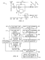
- FIG. 1 depicts a single silicon drift detector (SDD) device (100) as used in an embodiment of the present invention.
- SDD silicon drift detector
- Traditional SDD detector technology is utilized, wherein the collection of the charge in the SDD is realized on a single, small readout anode (108) using the lateral drift field within the detector.
- the resulting device has a very low capacitance ( ⁇ 1 pF), which improves the overall detector resolution even with large active areas (100 to 250 mm 2 ).
- the lateral drift field is obtained by integrating a chain of implanted resistive dividers (106) within the silicon substrate (110).
- a photon from a radiation event (110) enters the active area of the SDD (110) through the device's active area or "window" (104).
- FIG. 2 depicts such a combination (200).
- the scintillator (202) is optically coupled to the SDD (100).
- An incident gamma (204) enters and interacts with the scintillator material (202) causing incident photons (206). These photons then travel through the SDD window (104), ultimately creating an output signal at the readout anode (108).
- LaBr scintillator Although a LaBr scintillator is shown in the present embodiment, it is possible to utilize other scintillation materials instead.
- sodium iodide (NaI), cesium iodide (CsI), strontium iodide (SrI), mercuric iodide (HgI) and the like may also be utilized.
- the size of the SDD must be limited to ensure good energy resolution with short collection times.
- the area of each collection anode of the SDD device (100) is limited to less than 250 mm 2 to achieve this balance.
- a large area detector i.e., 5 to 50 cm 2
- Silicon photolithography techniques enable batch production of large silicon detectors subdivided into these different segments.
- FIG. 3 depicts an embodiment of such a combination (300).
- FIG. 3A depicts a simplified detail of an embodiment of the radiation sensor device of the present invention.
- two SDD segments (100) are combined and optically coupled (104) to the scintillator device (202).
- Each SDD segment features its own output anode (108) for extraction of the electrical output signal.
- SSDD segmented silicon drift detector
- an incident gamma (204) interacts with the scintillator (202) and causes photons to spread isotropically.
- the scintillation light is detected by the leftmost two SDD segments of the SSDD.
- An electrical signal is generated by these two segments with the outputs (108) supplying the signal to summation circuitry (302) for further processing.
- FIG. 3B depicts a cross-sectional diagram of the present embodiment of the SSDD device (101).
- the steering electrodes (106) comprise concentric rings around the output anodes (108).
- a circular SSDD configuration is depicted, other shapes may be utilized and are within the scope of the claims.
- the partial energies collected by every segment anodes can be summed by either analog or digital means to determine the total energy collected by the sensor after the detection of one event.
- the partial energies arising from each segment are linearly correlated with pulse or step heights coming out of each ASIC preamplifier-filter unit coupled to each drift segment.
- simple analog adder circuits may be utilized.
- the summed signal may then be sent to a single digitizing device, such as a multichannel analyzer (MCA), and then to a spectrum analysis device that is operable on the local processor.
- MCA multichannel analyzer
- the analog signals coming from each segment output anode may be multiplexed to one single digitizing device, such as an MCA, or sent in parallel to dedicated digitizing devices. If dedicated digitizing devices are utilized, the outputs of these digitizing devices may be multiplexed to the spectrum analysis device for final processing.
- time stamped addition Digitally summing the partial energies of several outputs collected in a defined time frame (called time stamped addition) reduces the low energy background signal and provides a better estimation of the integrals of peaks occurring at low energies than in the case of a simple analog addition of partial energies.
- the SSDD is utilized to extend the low energy range of the detector. This is accomplished by exposing the side comprising the "anode” (108) and the resistive dividers (106) to the irradiation of gamma and X rays, placing the scintillator material on the non-irradiated side (or back side) of the detector. In doing so, discrimination between low energy X-rays or alpha and beta rays that are directly absorbed in the semiconductor material and gamma rays scintillated in the scintillator is possible.
- An X-ray detected in the semiconductor will be absorbed in one single segment and will not be detected in other segments, while a gamma ray causing scintillation will generate events in all segments.
- Coincident events detected in several segment channels in the time stamped files will be associated with a high energy gamma event while events detected on a single segment or channel will be associated with a low energy X ray event (under 60 keV) or an alpha or beta event. Accordingly, when analyzing time stamped digitized information for all the segments of the detector and differentiating correlated events and non correlated events, it is possible to differentiate scintillated events from direct X-ray, alpha or beta ray absorption. This extends the low energy range of the sensor device.
- FIG. 4 A portion of the SSDD sensor processing circuitry of the present embodiment is depicted in FIG. 4 .
- This figure shows a basic schematic of the input portion of the basic anode output readout circuitry.
- the circuit shown is what can be utilized per anode, or group of anodes. For best performance, one such readout circuit must be attached to each SDD segment anode (i.e., one "channel"). Therefore, for the five segments depicted in FIG. 3 , five such circuits (400) must be utilized (five channels).
- the SDD (200, 406) connects to a voltage biasing network (404) and to an integrator circuit (414).
- the integrator circuit (414) is further controlled by a comparator (410) and a switch (408).
- the switch (408) is controlled by a monostable device (412) that periodically resets the amplifier output (416).
- the output of the readout circuit (416) is then fed to additional amplifier stages and signal processing stages. While a transistor reset preamplifier circuit is utilized in the present embodiment, it is important to note that other types of preamplifiers may also be utilized and are within the scope as claimed.
- the sensor processing circuitry of the present embodiment is designed to utilize numerous other detectors as well, such as the germanium and silicon variety. Operational characteristics of the available detectors include: Detector Detector Capacitance (pF) JFET C gs (pF) JFET g m (mS) Preamp Noise ( e rms ) Preamp Noise Slope ( ⁇ rms / pF) System Noise Ge (Std) 15 to 32 8 45 90.0 to 171 4.8 25 15 Ge (Well) 30 to 39 8 45 140 to 203 7.0 25 15 Ge (XtRa, REGe) 16 to 29 8 45 92.8 to 156 4.8 25 15 Ge (BEGe) 2 to 3 25 15 47.1 to 69.3 1.8 4 6 0.7 8 4 40 8 45 Ge (LEGe) 0.3 to 3 4 6 17.1 to 55.0 1.4 0.7 8 4 40 0.9 11 Ge (Ultra LEGe) 0.2 0.9 11 10.7 to 14.3 PLESi 0.4 0.7 8 7.
- DSP digital signal processor
- ASIC application specific integrated circuit
- the radiation detection apparatus employs a high-quality spectroscopic analysis device.
- spectroscopic analysis device may utilize a processing device that is capable of executing program instructions, an ASIC, or a dedicated programmable logic device such as a field programmable gate array (FPGA) or complex programmable logic device (CPLD).
- FPGA field programmable gate array
- CPLD complex programmable logic device
- an FPGA is employed (504) to perform the spectroscopic analysis using predefined algorithms (506) on the sensor outputs.
- the spectrometer (504) is able to adjust the parameters of the analysis algorithm (506), including response calibrations and nuclide libraries, based on measured spectral data as well as explicit knowledge of the measurement conditions.
- the parameters of the analysis algorithm (506) including response calibrations and nuclide libraries, based on measured spectral data as well as explicit knowledge of the measurement conditions.
- FIG. 5 depicts the entire system block diagram, wherein the sensor device (200) is followed by the sensor processing circuitry (e.g., the circuitry connecting the anodes to the preamplifier (400) and ASIC (502) or other similar configuration containing preamplifiers), which is followed by the spectroscopic analysis device (504 and 506).
- the sensor processing circuitry e.g., the circuitry connecting the anodes to the preamplifier (400) and ASIC (502) or other similar configuration containing preamplifiers
- the spectroscopic analysis device 504 and 506
- FIG. 6 depicts a logic flow diagram describing the spectral analysis steps performed by an embodiment of the present invention. Processing starts with a detected radiation event (602) that is conditioned by the analog preamplification (604) and subsequent digital processing circuitry (606). This sensor processing circuitry then determines the energy of each detected event (608). Given a set of acquired system events, a spectrum is generated as an energy-dependent histogram. The system has a set of stored calibrations, characterizing the system energy and peak shape responses based upon the selection of an application to be run on the device (612). The candidate nuclide physics data (intrinsic emission energies and probabilities) and specific geometry response information are input to the analysis based upon the application selected (614).
- the analysis determines the maximum likelihood match between the measured spectrum and the nuclide identity and activity as interpreted via the calibrations and other physics data (610).
- the nuclide analysis results are then interpreted based on the selected application (616) to yield the most appropriate output for display (618).
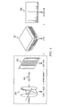
- FIG. 7 depicts an end product that incorporates all aspects of an embodiment of the present invention.
- the large SSDD sensor (702) is attached to the body of a handheld device (704) having a readily accessible control pad (706).
- a large readout (708) allows the operator to view and configure the device as well as to read the resulting spectroscopic analysis details.
- the present embodiment allows the implementation of specific algorithms, based on novel spectroscopy approaches with excellent NID (Nuclide Identification) performance that is compliant with ANSI standards. This embodiment also enables a high level of customization where different variables must be taken into account to reach good analysis results (radiation background, presence of overlaps of photoelectron peaks or multiplets, scattering, secondary induced reactions, temperature etc ).
- NID Nuclide Identification
- the radiation detection apparatus of the present invention incorporates networking capabilities that allow for a distributed network of independent intelligent sensors communicating with one supervisory controller unit.
- the supervisory control unit may be a standalone device that controls the independent sensors, or it may be incorporated into one of the sensors.
- the network enables localization and tracing as a function of time next to the identification of the radiation.
- the combination of the very compact intelligent sensor easily deployable in any location and the multiplication option of the intelligent sensor to a distributed network introduce a new way of analyzing and monitoring radiation.
- TCP/IP also allows placement of groups of sensors at a remote location and monitoring of the devices over the Internet.
- While the present embodiment primarily addresses use of a scintillator material for radiation detection, the same techniques also apply to other gamma and alpha spectroscopic detector materials, such as those consisting of germanium, silicon, CdTe, and CdZnTe. These semiconductor radiation detectors typically feature a single output anode, and convert a detected radiation event to an analog electrical signal at this output. In such an embodiment the output signal is supplied to the sensor processing circuitry and, subsequently, to the spectrum analysis device for final analysis.
- FIG. 8 depicts some of the areas in which the detection device incorporating the present invention may be utilized.
- the present embodiment and others are sufficiently flexible to allow use in mining operations (802) (i.e., area monitoring, exploration, down hole monitoring, material sorting, etc.); nuclear reactor facilities (804) (i.e., safeguards, area monitoring, spent fuel monitoring, pipe monitoring, burn up, RMS, etc.); nuclear fuel service and disposal facilities (806) (i.e., decontamination and decommissioning, area monitoring, dry fuel storage, etc.); nuclear fuel fabrication facilities (808) (i.e., area monitoring, on-line safeguards, hold up, pin fuel assembly, in-glove box, magazine counters, etc.); and fuel enrichment facilities (810) (i.e., area monitoring, cascade, online safeguards, etc.).
- the detector material may be chosen depending upon the requirements for the area in which the device is to be used.
- a radiation detection apparatus comprising: a radiation sensor device for detecting radiation events, the sensor device comprising: a scintillator device responsive to the radiation events; and one or more segmented silicon drift detector (SSDD) devices optically coupled to the scintillator device, wherein each SSDD device includes an output anode for each segment; and sensor processing circuitry coupled with each of the one or more silicon drift detector device output anodes, wherein each output can be processed simultaneously by the sensor processing circuitry.
- SSDD segmented silicon drift detector
- the radiation detection apparatus of statement 1 the apparatus further comprising: a spectroscopic analysis device coupled with the sensor processing circuitry for computing spectral data associated with the radiation detection event.
- each SSDD device comprises a plurality of output anodes and one collective steering cathode for all anodes.
- the sensor processing circuitry comprises an embedded computer processing device capable of executing stored program instructions that allow identification of the radionuclide that triggered the radiation detection event.
- the sensor processing circuitry comprises an ASIC device coupled to the SSDD output anodes, and wherein the ASIC device can process each of the detector outputs simultaneously.
- the radiation detection apparatus of statement 1 further comprising: a networking device through which the apparatus may communicate with other like apparatuses.
- the radiation detection apparatus of statement 1 further comprising: a networking device through which the apparatus may communicate with a supervisory control unit to form a part of a distributed network of like apparatuses.
- the spectroscopic analysis device is capable of executing program instructions, the program steps comprising: accumulating the output signal from each of the SSDD devices; generating a spectral histogram based upon the accumulated output signals; analyzing the spectral histogram with respect to interpreted known radionuclide responses; and identifying a detected radionuclide based upon a statistical analysis of the likelihood of a match between the spectral histogram and the interpreted radionuclide response.
- a method for reducing the influence of low energy background radiation during radiation detection events in a scintillator-equipped radiation detection apparatus comprising: optically coupling a plurality of segmented silicon drift detector (SSDD) devices to the scintillator material, wherein each SSDD device includes at least one output anode per segment; detecting radiation events within the scintillator material; accumulating the output signal from each of the output anodes; correlating the accumulated output signals with respect to the time that each output signal was obtained; and determining if the radiation detection event was detected by either all or less than all SSDD devices.
- SSDD segmented silicon drift detector
- each SSDD device comprises a plurality of output anodes and one collective steering cathode for all anodes.
- a method for extending the low energy range of a scintillator-equipped radiation detection apparatus comprising: optically coupling a plurality of segmented silicon drift detector (SSDD) devices to the scintillator material, wherein each SSDD device includes one output anode per segment; detecting radiation events within the scintillator material; detecting radiation events within the SSDD devices; accumulating the output signal from each of the output anodes; correlating the accumulated output signals with respect to the time that each output signal was obtained; and determining if the radiation detection event was detected by either one or more than one SSDD device.
- SSDD segmented silicon drift detector
- each SSDD device comprises a plurality of output anodes and one collective steering cathode for all anodes.
Landscapes
- Physics & Mathematics (AREA)
- Spectroscopy & Molecular Physics (AREA)
- Health & Medical Sciences (AREA)
- Life Sciences & Earth Sciences (AREA)
- General Physics & Mathematics (AREA)
- High Energy & Nuclear Physics (AREA)
- Molecular Biology (AREA)
- Measurement Of Radiation (AREA)
Applications Claiming Priority (3)
| Application Number | Priority Date | Filing Date | Title |
|---|---|---|---|
| US17034009P | 2009-04-17 | 2009-04-17 | |
| US22618509P | 2009-07-16 | 2009-07-16 | |
| US12/554,716 US20100264319A1 (en) | 2009-04-17 | 2009-09-04 | Intelligent Sensor Platform |
Publications (2)
| Publication Number | Publication Date |
|---|---|
| EP2246711A2 true EP2246711A2 (fr) | 2010-11-03 |
| EP2246711A3 EP2246711A3 (fr) | 2013-11-27 |
Family
ID=42767963
Family Applications (1)
| Application Number | Title | Priority Date | Filing Date |
|---|---|---|---|
| EP09169667.4A Withdrawn EP2246711A3 (fr) | 2009-04-17 | 2009-09-07 | Plate-forme de capteur intelligent |
Country Status (2)
| Country | Link |
|---|---|
| US (1) | US20100264319A1 (fr) |
| EP (1) | EP2246711A3 (fr) |
Cited By (5)
| Publication number | Priority date | Publication date | Assignee | Title |
|---|---|---|---|---|
| WO2012123404A1 (fr) * | 2011-03-14 | 2012-09-20 | Societe Franco-Belge De Fabrication De Combustibles - Fbfc | Dispositif et procede de spectrometrie photonique, procede de calibrage du dispositif et utilisation du dispositif |
| US9581703B2 (en) | 2011-03-14 | 2017-02-28 | Areva Np | Photonic spectrometry device, corresponding method, and use of the device |
| FR3044105A1 (fr) * | 2015-11-25 | 2017-05-26 | Canberra Ind Inc | |
| CN108280429A (zh) * | 2018-01-24 | 2018-07-13 | 北京中科核安科技有限公司 | 基于特征峰匹配的核素识别方法、装置和计算机可读介质 |
| WO2021139020A1 (fr) * | 2020-01-12 | 2021-07-15 | 兰州大学 | Système et procédé de détection à paramètres multiples pour la radioactivité de déchets de démantèlement d'installation nucléaire dans un trou de forage |
Families Citing this family (9)
| Publication number | Priority date | Publication date | Assignee | Title |
|---|---|---|---|---|
| EP2275837A3 (fr) * | 2009-07-16 | 2014-02-26 | Canberra Industries, Inc. | Détecteur de dérive au silicium simplifié et détecteur de neutrons enveloppant |
| EP2629118A3 (fr) * | 2012-02-15 | 2017-09-06 | CSEM Centre Suisse d'Electronique et de Microtechnique SA - Recherche et Développement | Détecteur de rayons x à haute sensibilité |
| GB2526578B (en) * | 2014-05-28 | 2021-08-04 | Soletanche Freyssinet Sas | Radioactive material assaying |
| CN104199076B (zh) * | 2014-09-12 | 2017-03-15 | 北京东方惠尔图像技术有限公司 | 辐射提示方法和装置 |
| GB2569371B (en) * | 2017-12-15 | 2022-01-12 | Lightpoint Medical Ltd | Direct detection and imaging of charged particles from a radiopharmaceutical |
| CN111373287B (zh) * | 2017-12-15 | 2025-01-14 | 株式会社堀场制作所 | 放射线检测器和放射线检测装置 |
| CN109671798B (zh) * | 2018-12-21 | 2020-08-04 | 中国科学院微电子研究所 | 漂移探测器及其制作方法 |
| CN109671797B (zh) * | 2018-12-21 | 2020-08-04 | 中国科学院微电子研究所 | 漂移探测器及其制作方法 |
| CN110265511B (zh) * | 2019-05-22 | 2021-01-26 | 李正 | 大面积双面硅漂移探测器的加工工艺 |
Family Cites Families (5)
| Publication number | Priority date | Publication date | Assignee | Title |
|---|---|---|---|---|
| DE3571726D1 (en) * | 1984-04-25 | 1989-08-24 | Josef Kemmer | Large-surface low-capacity semi-conductor radiation detector |
| WO2000028351A1 (fr) * | 1998-11-09 | 2000-05-18 | Iwanczyk Jan S | Detecteur de rayons gamma utilisant des scintillateurs couples a des photodetecteurs a derive a semi-conducteur |
| US6574629B1 (en) * | 1998-12-23 | 2003-06-03 | Agfa Corporation | Picture archiving and communication system |
| DE10213812B4 (de) * | 2002-03-27 | 2007-03-29 | MAX-PLANCK-Gesellschaft zur Förderung der Wissenschaften e.V. | Leitungsüberführung für einen Halbleiter-Detektor |
| DE10260229B3 (de) * | 2002-12-20 | 2005-08-18 | MAX-PLANCK-Gesellschaft zur Förderung der Wissenschaften e.V. | Halbleiter-Detektor mit optimiertem Strahlungseintrittsfenster |
-
2009
- 2009-09-04 US US12/554,716 patent/US20100264319A1/en not_active Abandoned
- 2009-09-07 EP EP09169667.4A patent/EP2246711A3/fr not_active Withdrawn
Non-Patent Citations (3)
| Title |
|---|
| BOSLAU O ET AL: "Large-Area Silicon Drift Detectors for New Applications in Nuclear Medicine Imaging", IEEE TRANSACTIONS ON NUCLEAR SCIENCE, IEEE SERVICE CENTER, NEW YORK, NY, US, vol. 51, no. 4, 1 August 2004 (2004-08-01) , pages 1631-1635, XP011116236, ISSN: 0018-9499, DOI: 10.1109/TNS.2004.832666 * |
| FIORINI C ET AL: "Semiconductor drift detectors for X- and gamma-ray spectroscopy and imaging", NUCLEAR INSTRUMENTS & METHODS IN PHYSICS RESEARCH, SECTION - B:BEAM INTERACTIONS WITH MATERIALS AND ATOMS, ELSEVIER, AMSTERDAM, NL, vol. 266, no. 10, 1 May 2008 (2008-05-01), pages 2173-2181, XP022695280, ISSN: 0168-583X, DOI: 10.1016/J.NIMB.2008.02.059 [retrieved on 2008-03-06] * |
| HOLL P ET AL: "A 55 cm<2> cylindrical silicon drift detector", NUCLEAR INSTRUMENTS & METHODS IN PHYSICS RESEARCH. SECTION A: ACCELERATORS, SPECTROMETERS, DETECTORS, AND ASSOCIATED EQUIPMENT, ELSEVIER BV * NORTH-HOLLAND, NETHERLANDS, vol. 377, no. 2, 1 August 1996 (1996-08-01), pages 367-374, XP004008280, ISSN: 0168-9002, DOI: 10.1016/0168-9002(96)00027-7 * |
Cited By (11)
| Publication number | Priority date | Publication date | Assignee | Title |
|---|---|---|---|---|
| WO2012123404A1 (fr) * | 2011-03-14 | 2012-09-20 | Societe Franco-Belge De Fabrication De Combustibles - Fbfc | Dispositif et procede de spectrometrie photonique, procede de calibrage du dispositif et utilisation du dispositif |
| FR2972811A1 (fr) * | 2011-03-14 | 2012-09-21 | Franco Belge Combustibles | Dispositif et procede de spectrometrie photonique, procede de calibrage du dispositif et utilisation du dispositif |
| CN103534611A (zh) * | 2011-03-14 | 2014-01-22 | 阿海珐核能公司 | 光子能谱装置和方法,校准该装置的方法以及该装置的用途 |
| US9400336B2 (en) | 2011-03-14 | 2016-07-26 | Areva Np | Photonic spectrometry device and method, method for calibrating the device, and use of the device |
| US9581703B2 (en) | 2011-03-14 | 2017-02-28 | Areva Np | Photonic spectrometry device, corresponding method, and use of the device |
| CN103534611B (zh) * | 2011-03-14 | 2017-04-05 | 阿海珐核能公司 | 光子能谱装置和方法,校准该装置的方法以及该装置的用途 |
| FR3044105A1 (fr) * | 2015-11-25 | 2017-05-26 | Canberra Ind Inc | |
| US10139496B2 (en) | 2015-11-25 | 2018-11-27 | Mirion Technologies (Canberra), Inc. | Multi-radiation identification and dosimetry system and method |
| CN108280429A (zh) * | 2018-01-24 | 2018-07-13 | 北京中科核安科技有限公司 | 基于特征峰匹配的核素识别方法、装置和计算机可读介质 |
| CN108280429B (zh) * | 2018-01-24 | 2020-06-26 | 北京中科核安科技有限公司 | 基于特征峰匹配的核素识别方法、装置和计算机可读介质 |
| WO2021139020A1 (fr) * | 2020-01-12 | 2021-07-15 | 兰州大学 | Système et procédé de détection à paramètres multiples pour la radioactivité de déchets de démantèlement d'installation nucléaire dans un trou de forage |
Also Published As
| Publication number | Publication date |
|---|---|
| EP2246711A3 (fr) | 2013-11-27 |
| US20100264319A1 (en) | 2010-10-21 |
Similar Documents
| Publication | Publication Date | Title |
|---|---|---|
| EP2246711A2 (fr) | Plate-forme de capteur intelligent | |
| US8063380B2 (en) | Semiconductor crystal high resolution imager | |
| CN110941007B (zh) | 核能谱的处理方法和设备 | |
| CA1219086A (fr) | Appareil d'imagerie a detecteurs de rayonnement | |
| US20170212251A1 (en) | Multiple spatial resolution scintillation detectors | |
| JP7026443B2 (ja) | 放射性ダストモニタ | |
| EP1840597A2 (fr) | Procédé d'étalonnage de l'énergie et appareil de détection de la radiation et d'imagerie radiologique | |
| Vaquero et al. | Performance characteristics of a compact position-sensitive LSO detector module | |
| US8648314B1 (en) | Fast neutron imaging device and method | |
| CN102670232A (zh) | 正电子发射计算机断层摄影装置、以及通过它执行的方法 | |
| JP2008190901A (ja) | 陽電子放出型断層撮影装置 | |
| CN114740521A (zh) | 一种基于β-γ符合的探测系统及方法 | |
| CN119471768A (zh) | 一种可核素识别的个人剂量仪 | |
| JP7100549B2 (ja) | 高エネルギ線検出器および断層画像取得装置 | |
| JP2003315465A (ja) | 多層放射線検出器を用いたガンマ線源の距離測定装置 | |
| Morishita et al. | Development of a Gd₂Si₂O₇ (GPS) scintillator-based alpha imaging detector for rapid plutonium detection in high-radon environments | |
| JP3622967B1 (ja) | 放射線撮像装置 | |
| Pavelic et al. | A technology overview of active ionizing radiation dosemeters for photon fields | |
| JP7058564B2 (ja) | アルファ線用放射性ダストモニタ | |
| JP7320556B2 (ja) | ピクセルのサブセットからの光子相互作用特性 | |
| Cassette et al. | Development of portable liquid scintillation counters for on-site primary measurement of radionuclides using the triple-to-double coincidence ratio method | |
| Azimi et al. | Compact Beta-Gamma Radioxenon Detection System with Improved Energy Resolution Using PIPS Detector: SA Azimi et al. | |
| González et al. | Performance Comparison of a Large Volume CZT Semiconductor Detector and a LaBr $ _3 $(Ce) Scintillator Detector | |
| KR101702832B1 (ko) | Multi-SCA 감마선 방사성 추적자 데이터 수집장치 | |
| Cinti et al. | Custom breast phantom for an accurate tumor SNR analysis |
Legal Events
| Date | Code | Title | Description |
|---|---|---|---|
| PUAI | Public reference made under article 153(3) epc to a published international application that has entered the european phase |
Free format text: ORIGINAL CODE: 0009012 |
|
| AK | Designated contracting states |
Kind code of ref document: A2 Designated state(s): AT BE BG CH CY CZ DE DK EE ES FI FR GB GR HR HU IE IS IT LI LT LU LV MC MK MT NL NO PL PT RO SE SI SK SM TR |
|
| PUAL | Search report despatched |
Free format text: ORIGINAL CODE: 0009013 |
|
| AK | Designated contracting states |
Kind code of ref document: A3 Designated state(s): AT BE BG CH CY CZ DE DK EE ES FI FR GB GR HR HU IE IS IT LI LT LU LV MC MK MT NL NO PL PT RO SE SI SK SM TR |
|
| RIC1 | Information provided on ipc code assigned before grant |
Ipc: G01T 1/20 20060101AFI20131018BHEP |
|
| 17P | Request for examination filed |
Effective date: 20140725 |
|
| RBV | Designated contracting states (corrected) |
Designated state(s): AT BE BG CH CY CZ DE DK EE ES FI FR GB GR HR HU IE IS IT LI LT LU LV MC MK MT NL NO PL PT RO SE SI SK SM TR |
|
| STAA | Information on the status of an ep patent application or granted ep patent |
Free format text: STATUS: THE APPLICATION IS DEEMED TO BE WITHDRAWN |
|
| 18D | Application deemed to be withdrawn |
Effective date: 20140401 |