EP2246781B1 - Umkonfigurierbare einrichtung - Google Patents
Umkonfigurierbare einrichtung Download PDFInfo
- Publication number
- EP2246781B1 EP2246781B1 EP09707098.1A EP09707098A EP2246781B1 EP 2246781 B1 EP2246781 B1 EP 2246781B1 EP 09707098 A EP09707098 A EP 09707098A EP 2246781 B1 EP2246781 B1 EP 2246781B1
- Authority
- EP
- European Patent Office
- Prior art keywords
- command
- data
- matrix
- data flow
- processing elements
- Prior art date
- Legal status (The legal status is an assumption and is not a legal conclusion. Google has not performed a legal analysis and makes no representation as to the accuracy of the status listed.)
- Active
Links
Images


Classifications
-
- G—PHYSICS
- G06—COMPUTING OR CALCULATING; COUNTING
- G06F—ELECTRIC DIGITAL DATA PROCESSING
- G06F15/00—Digital computers in general; Data processing equipment in general
- G06F15/76—Architectures of general purpose stored program computers
- G06F15/80—Architectures of general purpose stored program computers comprising an array of processing units with common control, e.g. single instruction multiple data processors
- G06F15/8007—Architectures of general purpose stored program computers comprising an array of processing units with common control, e.g. single instruction multiple data processors single instruction multiple data [SIMD] multiprocessors
-
- G—PHYSICS
- G06—COMPUTING OR CALCULATING; COUNTING
- G06F—ELECTRIC DIGITAL DATA PROCESSING
- G06F15/00—Digital computers in general; Data processing equipment in general
- G06F15/76—Architectures of general purpose stored program computers
- G06F15/78—Architectures of general purpose stored program computers comprising a single central processing unit
- G06F15/7867—Architectures of general purpose stored program computers comprising a single central processing unit with reconfigurable architecture
Definitions
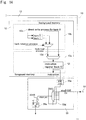
- a typical command transmitted by the command transmitting system is a stop command for stopping a clock of the processing elements.
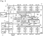
- the bank control unit 29b of the LDB element is equipped with a function as a command generating unit and includes a function (functional unit) that generates and outputs a flow stop signal.
- a function functional unit
- the bank control unit 29b of the LDB element When it is desirable to stop a data flow (data path) that carries out processing on data outputted (read) from the LDB element, the bank control unit 29b of the LDB element generates and outputs a flow stop command (stop command, flow stop request) Cs that includes an EID showing the data flow reconfigured in the PE matrix 10 for such processing and a flow stop signal.
- the LDB element is capable of stopping the desired data flow that reads out data via an output control unit 122.
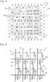
- all of the PEs disposed in the segments a1 to a4 are controlled in the next clock cycle by a command latched in the command register 53 of each segment. Therefore, according to the command transmitting system 50, all of the PEs disposed in the PE matrix 10 are controlled by a command in synchronization in the second clock cycle after the command has been latched by the command register 59f of the command outputting unit 59 of the STB.
- the bank control unit 29b and the command generating unit 69 that are the units that generate the flow stop command in an element such as the LDB and RAM may be further equipped with a function (functional unit) that removes or does not generate a flow stop in order to output the final data. This is because there is the possibility of a data flow becoming deadlocked due to the amount of remaining data in the storage region 29a that functions as a FIFO not increasing after the final data has been received.
- the flow stop command Cs (flow stop request) outputted by the bank controller 29b is latched (obtained) by the command register (FF) 63 of each segment of the command collecting system 60 via the first level command collecting matrix 61 in cycle t(-3). That is, the command Cs is collected by a register 63 of the command collecting system 60.
- the command Cs collected in the register 63 of the command collecting system 60 is obtained by the output register (FF) 59f of the command outputting unit 59 of the STB via the second level command collecting matrix 62 in cycle t(-2). That is, the command Cs is collected in the register 59f.
- DLE elements and RAM elements that include a function as a FIFO in the data flow to control an upstream and/or a downstream data flow in the same way.
- a flow stop request with a number corresponding to its own EID or the EID of the upstream data flow will be outputted at timing when it appears that the FIFO will become full due to writing by the upstream data flow.
- the DLE element or RAM element also outputs a flow stop request (flow stop command) with the EID of the downstream data flow to the downstream data flow depending on the amount of data remaining in the FIFO. This makes it possible to prevent the supplying of bubbles to the downstream data flow from the outset. Also, as one example, it is possible to indicate whether a read is possible using the carry signal of the PE 17. If the carry is "1", this shows that there is data to be read out to the FIFO. By using this signal downstream, it is possible to carry out a read when circumstances are favorable.
Landscapes
- Engineering & Computer Science (AREA)
- Computer Hardware Design (AREA)
- Theoretical Computer Science (AREA)
- Physics & Mathematics (AREA)
- General Engineering & Computer Science (AREA)
- General Physics & Mathematics (AREA)
- Computing Systems (AREA)
- Multi Processors (AREA)
- Logic Circuits (AREA)
Claims (9)
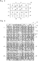
- Vorrichtung (1) aufweisend einen rekonfigurierbaren Abschnitt, mit einer Vielzahl an Verarbeitungselementen (17), die so angeordnet sind, dass sie in eine Vielzahl an Segmenten unterteilt sind, und eine Routingmatrix zum Verbinden der Vielzahl an Verarbeitungselementen, wobei ein Datenfluss in dem rekonfigurierbaren Abschnitt, unter Verwendung wenigstens einiger der Vielzahl an Verarbeitungselementen und wenigstens eines Teils der Routingmatrix, rekonfiguriert wird,
wobei die Routingmatrix aufweist: eine Routing-Matrix (21) der ersten Ebene, die in jedem Segment enthaltene Verarbeitungselemente innerhalb eines Bereichs einer ersten Verzögerung verbindet, wobei die erste Verzögerung ein Ein-Takt-Zyklus ist; und
eine Routing-Matrix (22) der zweiten Ebene, welche Verarbeitungselemente, die in verschiedenen Segmenten enthalten sind, innerhalb einer zweiten Verzögerung , die sich von der ersten Verzögerung unterscheidet, verbindet, wobei die zweite Verzögerung zusätzlich zur ersten Verzögerung eine zusätzliche Verzögerung von mindestens einem Ein-Takt-Zyklus enthält, wobei die Vorrichtung ferner ein Befehlsübertragungssystem (50) enthält, welches Befehle an jedes Verarbeitungselement, das in dem rekonfigurierbaren Abschnitt enthalten ist, überträgt, und
das Befehlsübertragungssystem (50) aufweist:ein Übertragungsbefehlsregister (53), das in jedem Segment vorgesehen ist und von allen Verarbeitungselementen in jedem Segment gemeinsam genutzt wird;eine Befehlsübertragungsmatrix (51) der ersten Ebene, die das Übertragungsbefehlsregister (53) und alle Verarbeitungselemente (17) in jedem Segment innerhalb der ersten Verzögerung verbindet; undeine Befehlsübertragungsmatrix (52) der zweiten Ebene, die Übertragungsbefehlsregister (53) aus der Vielzahl an Segmenten verbindet, und,eine Befehlsausgabeeinheit (59), welche Befehle zur Übertragung der Befehle an alle Verarbeitungselemente in jedem Segment synchron mit einer vorbestimmten Latenz über die Befehlsübertragungsmatrix (52) der zweiten Ebene, das Übertragungsbefehlsregister (53) und die Befehlsübertragungsmatrix (51) der ersten Ebene mit einer Verzögerung, die sich von der ersten Verzögerung unterscheidet, ausgibt,wobei zumindest ein Teil der Verarbeitungselemente (17) aus der Vielzahl an Verarbeitungselementen aufweist:Befehlserzeugungseinheiten (69);Ausgabeschnittstellenelemente, wobei jedes Ausgabeschnittstellenelement eine Speichereinheit enthält, die vorübergehend eine Ausgabe speichert, welche durch einen Datenfluss verarbeitet wird, der in dem rekonfigurierbaren Abschnitt konfiguriert ist; undEingabeschnittstellenelemente, wobei jedes Eingabeschnittstellenelement eine Speichereinheit enthält, die Eingabedaten vorübergehend in einem Datenfluss speichert, der in dem rekonfigurierbaren Abschnitt konfiguriert wurde, und wobeidie Vorrichtung weiter aufweist:ein Befehlssammelsystem (60), das von jeder befehlserzeugenden Einheit (69) erzeugte Befehle in die befehlsausgebende Einheit sammelt,wobei das Befehlssammelsystem (60) aufweist:ein Sammelbefehlsregister (63), das in jedem Segment vorgesehen ist;eine Befehlssammelmatrix (61) der ersten Ebene, die das Sammelbefehlsregister (63) und den mindestens einen Teil der Verarbeitungselemente in jedem Segment innerhalb der ersten Verzögerung verbindet; undeine Befehlssammelmatrix (62) der zweiten Ebene, die die Befehlssammelregister (63) aus der Vielzahl an Segmenten und die Befehlsausgabeeinheit mit einer Verzögerung verbindet, die sich von der ersten Verzögerung unterscheidet, damit alle Verarbeitungselemente in jedem Segment eine einheitliche Latenz von der Ausgabe eines Befehls bis zum Empfang dieses Befehls haben,wobei die durch das Befehlsübertragungssystem (50) übertragenen Befehle einen Stoppbefehl enthalten, der einen Takt jedes Verarbeitungselements stoppt, undwobei eine Befehlserzeugungseinheit (69), die in jedem Eingabeschnittstellenelement enthalten ist, eine Funktion aufweist, die zum Ausgeben des Stoppbefehls geeignet ist, wenn eine in der Speichereinheit verbleibende Datenmenge, gleich einer Datenmenge geworden ist, die durch den Datenfluss verbraucht wird, verbraucht während Zyklen, wenn ein Befehl durch das Befehlssammelsystem (60) und das Befehlsübertragungssystem (50) übertragen wird. - Vorrichtung nach Anspruch 1,
wobei eine Befehlserzeugungseinheit (69), die in jedem Eingabeschnittstellenelement enthalten ist, eine Funktion aufweist, die, wenn sich endgültige Daten in der Speichereinheit befinden, geeignet ist, den Stoppbefehl nicht auszugeben. - Vorrichtung nach Anspruch 1,
wobei der zumindest eine Teil der Verarbeitungselemente Elemente vom Datenspeichertyp enthält, wobei jedes Element vom Datenspeichertyp eine Speichereinheit aufweist, die temporär Zwischendaten speichert, die durch den Datenfluss verarbeitet werden, und
eine Befehlserzeugungseinheit (69), die in jedem Element vom Datenspeichertyp enthalten ist, und eine Funktion enthält, die geeignet ist, den Stoppbefehl auszugeben, wenn eine in der Speichereinheit verbleibende Datenmenge eine Datenmenge geworden ist, die während der Zyklen durch den Datenfluss verbraucht wird, und verbraucht wird, wenn ein Befehl durch das Befehlssammelsystem (60) und das Befehlsübertragungssystem (50) übertragen wird. - Vorrichtung nach Anspruch 3,
wobei die Befehlserzeugungseinheit (69), die in jedem Element vom Datenspeichertyp enthalten ist, eine Funktion enthält, die, wenn sich endgültige Daten in der Speichereinheit befinden, geeignet ist, den Stoppbefehl nicht auszugeben. - Vorrichtung nach einem der vorhergehenden Ansprüche,
wobei die Vielzahl an Verarbeitungselementen Verarbeitungselemente enthält, die den Datenfluss durch Änderung von Funktionen rekonfigurieren. - Vorrichtung nach einem der vorhergehenden Ansprüche,
wobei die Routingmatrix eine Routingmatrix enthält, die den Datenfluss rekonfiguriert, indem sie diesbezüglich mindestens eine Verbindung ändert. - Vorrichtung nach einem der vorhergehenden Ansprüche,
wobei eine Vielzahl von Datenflüssen in dem rekonfigurierbaren Abschnitt rekonfiguriert werden, wobei die Vielzahl an Verarbeitungselementen, die in dem rekonfigurierbaren Abschnitt enthalten sind, Steuereinheiten aufweisen mit Identifikationsinformationen, die einen Datenfluss identifizieren, zu dem jeweilige Verarbeitungselemente gehören, und die Befehle, die durch das Befehlsübertragungssystem (50) übertragen werden, Identifikationsinformationen beinhalten. - Vorrichtung nach Anspruch 7,
wobei sich Identifikationsinformationen, die einen stromaufwärtigen Datenfluss eines eine Befehlserzeugungseinheit (69) aufweisenden Verarbeitungselements identifizieren, von Identifikationsinformationen unterscheiden, die einen stromabwärtigen Datenfluss des Verarbeitungselements identifizieren. - Vorrichtung nach einem der vorhergehenden Ansprüche,
wobei die Vorrichtung ferner einen Prozessor umfasst, der einen Befehl generiert, welcher über die Befehlsübertragungsmatrix (52) der zweiten Ebene übertragen wird, um einen in dem rekonfigurierbaren Abschnitt konfigurierten Datenfluss zu steuern.
Applications Claiming Priority (2)
| Application Number | Priority Date | Filing Date | Title |
|---|---|---|---|
| JP2008021546 | 2008-01-31 | ||
| PCT/JP2009/051491 WO2009096482A1 (ja) | 2008-01-31 | 2009-01-29 | 再構成可能なデバイス |
Publications (3)
| Publication Number | Publication Date |
|---|---|
| EP2246781A1 EP2246781A1 (de) | 2010-11-03 |
| EP2246781A4 EP2246781A4 (de) | 2012-01-11 |
| EP2246781B1 true EP2246781B1 (de) | 2020-12-09 |
Family
ID=40912827
Family Applications (1)
| Application Number | Title | Priority Date | Filing Date |
|---|---|---|---|
| EP09707098.1A Active EP2246781B1 (de) | 2008-01-31 | 2009-01-29 | Umkonfigurierbare einrichtung |
Country Status (7)
| Country | Link |
|---|---|
| US (1) | US20110047353A1 (de) |
| EP (1) | EP2246781B1 (de) |
| JP (1) | JP5170579B2 (de) |
| KR (1) | KR101265120B1 (de) |
| CN (1) | CN101983373B (de) |
| AU (1) | AU2009209933B2 (de) |
| WO (1) | WO2009096482A1 (de) |
Families Citing this family (7)
| Publication number | Priority date | Publication date | Assignee | Title |
|---|---|---|---|---|
| JP5711889B2 (ja) * | 2010-01-27 | 2015-05-07 | スパンション エルエルシー | リコンフィギュラブル回路および半導体集積回路 |
| JP5821332B2 (ja) * | 2011-06-30 | 2015-11-24 | 株式会社ソシオネクスト | リコンフィグ可能な集積回路装置 |
| US8860457B2 (en) * | 2013-03-05 | 2014-10-14 | Qualcomm Incorporated | Parallel configuration of a reconfigurable instruction cell array |
| US9537471B2 (en) * | 2015-02-09 | 2017-01-03 | Qualcomm Incorporated | Three dimensional logic circuit |
| CN106021145B (zh) * | 2016-05-25 | 2019-06-14 | 芯启源(上海)半导体科技有限公司 | 应用处理器、应用处理装置及命令执行方法 |
| US10402355B2 (en) | 2017-02-08 | 2019-09-03 | Texas Instruments Incorporated | Apparatus and mechanism to bypass PCIe address translation by using alternative routing |
| JP7433931B2 (ja) * | 2020-01-27 | 2024-02-20 | キヤノン株式会社 | 情報処理装置及びその制御方法及びプログラム |
Family Cites Families (12)
| Publication number | Priority date | Publication date | Assignee | Title |
|---|---|---|---|---|
| US5742180A (en) * | 1995-02-10 | 1998-04-21 | Massachusetts Institute Of Technology | Dynamically programmable gate array with multiple contexts |
| US6760743B1 (en) * | 2000-01-04 | 2004-07-06 | International Business Machines Corporation | Instruction memory system for multi-processor environment and disjoint tasks |
| US7380100B2 (en) * | 2001-09-07 | 2008-05-27 | Ipflex Inc. | Data processing system and control method utilizing a plurality of date transfer means |
| US7657861B2 (en) * | 2002-08-07 | 2010-02-02 | Pact Xpp Technologies Ag | Method and device for processing data |
| US7000091B2 (en) * | 2002-08-08 | 2006-02-14 | Hewlett-Packard Development Company, L.P. | System and method for independent branching in systems with plural processing elements |
| JP4664311B2 (ja) * | 2003-12-29 | 2011-04-06 | ザイリンクス インコーポレイテッド | カスケード接続するdspスライスを備えた集積回路 |
| US7207020B1 (en) * | 2004-02-09 | 2007-04-17 | Altera Corporation | Method and apparatus for utilizing long-path and short-path timing constraints in an electronic-design-automation tool |
| JP4446437B2 (ja) * | 2004-03-19 | 2010-04-07 | アイピーフレックス株式会社 | データ処理装置およびその制御方法 |
| JP4546775B2 (ja) * | 2004-06-30 | 2010-09-15 | 富士通株式会社 | 時分割多重処理可能なリコンフィギュラブル回路 |
| JP4720436B2 (ja) * | 2005-11-01 | 2011-07-13 | 株式会社日立製作所 | リコンフィギュラブルプロセッサまたは装置 |
| JP4936517B2 (ja) * | 2006-06-06 | 2012-05-23 | 学校法人早稲田大学 | ヘテロジニアス・マルチプロセッサシステムの制御方法及びマルチグレイン並列化コンパイラ |
| JP4451433B2 (ja) * | 2006-12-04 | 2010-04-14 | 株式会社リコー | 並列プロセッサ |
-
2009
- 2009-01-29 KR KR1020107018660A patent/KR101265120B1/ko active Active
- 2009-01-29 AU AU2009209933A patent/AU2009209933B2/en active Active
- 2009-01-29 WO PCT/JP2009/051491 patent/WO2009096482A1/ja not_active Ceased
- 2009-01-29 US US12/865,165 patent/US20110047353A1/en not_active Abandoned
- 2009-01-29 CN CN2009801118667A patent/CN101983373B/zh active Active
- 2009-01-29 EP EP09707098.1A patent/EP2246781B1/de active Active
- 2009-01-29 JP JP2009551576A patent/JP5170579B2/ja active Active
Non-Patent Citations (1)
| Title |
|---|
| None * |
Also Published As
| Publication number | Publication date |
|---|---|
| EP2246781A4 (de) | 2012-01-11 |
| KR101265120B1 (ko) | 2013-05-16 |
| EP2246781A1 (de) | 2010-11-03 |
| US20110047353A1 (en) | 2011-02-24 |
| KR20100122084A (ko) | 2010-11-19 |
| CN101983373A (zh) | 2011-03-02 |
| AU2009209933A1 (en) | 2009-08-06 |
| CN101983373B (zh) | 2013-04-17 |
| WO2009096482A1 (ja) | 2009-08-06 |
| AU2009209933B2 (en) | 2012-01-19 |
| JPWO2009096482A1 (ja) | 2011-05-26 |
| JP5170579B2 (ja) | 2013-03-27 |
Similar Documents
| Publication | Publication Date | Title |
|---|---|---|
| US12306783B2 (en) | Top level network and array level network for reconfigurable data processors | |
| EP2246781B1 (de) | Umkonfigurierbare einrichtung | |
| CN100414535C (zh) | 可重配置的集成电路器件 | |
| US3537074A (en) | Parallel operating array computer | |
| KR100288038B1 (ko) | 초대규모집적에 적합한 파이프라인 반도체장치 | |
| CN101925881B (zh) | 多处理器系统以及多处理器系统的同步方法 | |
| KR20010020545A (ko) | 재구성 가능한 컴퓨팅을 위한 집적 프로세서 및프로그래머블 데이터 경로 칩 | |
| US20250036591A1 (en) | Micro-network-on-chip and microsector infrastructure | |
| US20060004991A1 (en) | Semiconductor device | |
| US10659396B2 (en) | Joining data within a reconfigurable fabric | |
| US20180212894A1 (en) | Fork transfer of data between multiple agents within a reconfigurable fabric | |
| EP2132645A1 (de) | Datentransfernetzwerk und steuervorrichtung für ein system mit einem array von verarbeitungselementen, die jeweils entweder selbst- oder gemeinsam gesteuert sind | |
| US20060190701A1 (en) | Data processor | |
| US8320150B2 (en) | Structure and method for backing up and restitution of data | |
| CN109766293B (zh) | 连接芯片上fpga和人工智能模块的电路和系统芯片 | |
| CN106716336A (zh) | 在多处理器系统中的存储器管理 | |
| JP2008305215A (ja) | バスシステム | |
| JP4437439B2 (ja) | データ処理装置 | |
| US7149827B1 (en) | Methods and apparatus for tristate line sharing | |
| Baranwal et al. | PoCo: Extending Task-Parallel HLS Programming with Shared Multi-P ro ducer Multi-Co nsumer Buffer Support | |
| CN102184089B (zh) | 一种动态可重构处理器内数据流运转的方法 | |
| WO2019006119A1 (en) | COMBINING DATA IN A RECONFIGURABLE MATRIX |
Legal Events
| Date | Code | Title | Description |
|---|---|---|---|
| PUAI | Public reference made under article 153(3) epc to a published international application that has entered the european phase |
Free format text: ORIGINAL CODE: 0009012 |
|
| 17P | Request for examination filed |
Effective date: 20100730 |
|
| AK | Designated contracting states |
Kind code of ref document: A1 Designated state(s): AT BE BG CH CY CZ DE DK EE ES FI FR GB GR HR HU IE IS IT LI LT LU LV MC MK MT NL NO PL PT RO SE SI SK TR |
|
| AX | Request for extension of the european patent |
Extension state: AL BA RS |
|
| DAX | Request for extension of the european patent (deleted) | ||
| A4 | Supplementary search report drawn up and despatched |
Effective date: 20111213 |
|
| RIC1 | Information provided on ipc code assigned before grant |
Ipc: G06F 15/78 20060101ALI20111207BHEP Ipc: G06F 7/00 20060101AFI20111207BHEP |
|
| STAA | Information on the status of an ep patent application or granted ep patent |
Free format text: STATUS: EXAMINATION IS IN PROGRESS |
|
| 17Q | First examination report despatched |
Effective date: 20170315 |
|
| GRAP | Despatch of communication of intention to grant a patent |
Free format text: ORIGINAL CODE: EPIDOSNIGR1 |
|
| STAA | Information on the status of an ep patent application or granted ep patent |
Free format text: STATUS: GRANT OF PATENT IS INTENDED |
|
| INTG | Intention to grant announced |
Effective date: 20200721 |
|
| RIN1 | Information on inventor provided before grant (corrected) |
Inventor name: MATSUNO, HIROYUKI |
|
| GRAS | Grant fee paid |
Free format text: ORIGINAL CODE: EPIDOSNIGR3 |
|
| GRAA | (expected) grant |
Free format text: ORIGINAL CODE: 0009210 |
|
| STAA | Information on the status of an ep patent application or granted ep patent |
Free format text: STATUS: THE PATENT HAS BEEN GRANTED |
|
| AK | Designated contracting states |
Kind code of ref document: B1 Designated state(s): AT BE BG CH CY CZ DE DK EE ES FI FR GB GR HR HU IE IS IT LI LT LU LV MC MK MT NL NO PL PT RO SE SI SK TR |
|
| REG | Reference to a national code |
Ref country code: GB Ref legal event code: FG4D |
|
| REG | Reference to a national code |
Ref country code: AT Ref legal event code: REF Ref document number: 1344099 Country of ref document: AT Kind code of ref document: T Effective date: 20201215 Ref country code: CH Ref legal event code: EP |
|
| REG | Reference to a national code |
Ref country code: DE Ref legal event code: R096 Ref document number: 602009063155 Country of ref document: DE |
|
| REG | Reference to a national code |
Ref country code: IE Ref legal event code: FG4D |
|
| PG25 | Lapsed in a contracting state [announced via postgrant information from national office to epo] |
Ref country code: GR Free format text: LAPSE BECAUSE OF FAILURE TO SUBMIT A TRANSLATION OF THE DESCRIPTION OR TO PAY THE FEE WITHIN THE PRESCRIBED TIME-LIMIT Effective date: 20210310 Ref country code: FI Free format text: LAPSE BECAUSE OF FAILURE TO SUBMIT A TRANSLATION OF THE DESCRIPTION OR TO PAY THE FEE WITHIN THE PRESCRIBED TIME-LIMIT Effective date: 20201209 Ref country code: NO Free format text: LAPSE BECAUSE OF FAILURE TO SUBMIT A TRANSLATION OF THE DESCRIPTION OR TO PAY THE FEE WITHIN THE PRESCRIBED TIME-LIMIT Effective date: 20210309 |
|
| REG | Reference to a national code |
Ref country code: AT Ref legal event code: MK05 Ref document number: 1344099 Country of ref document: AT Kind code of ref document: T Effective date: 20201209 |
|
| PG25 | Lapsed in a contracting state [announced via postgrant information from national office to epo] |
Ref country code: LV Free format text: LAPSE BECAUSE OF FAILURE TO SUBMIT A TRANSLATION OF THE DESCRIPTION OR TO PAY THE FEE WITHIN THE PRESCRIBED TIME-LIMIT Effective date: 20201209 Ref country code: SE Free format text: LAPSE BECAUSE OF FAILURE TO SUBMIT A TRANSLATION OF THE DESCRIPTION OR TO PAY THE FEE WITHIN THE PRESCRIBED TIME-LIMIT Effective date: 20201209 Ref country code: BG Free format text: LAPSE BECAUSE OF FAILURE TO SUBMIT A TRANSLATION OF THE DESCRIPTION OR TO PAY THE FEE WITHIN THE PRESCRIBED TIME-LIMIT Effective date: 20210309 |
|
| REG | Reference to a national code |
Ref country code: NL Ref legal event code: MP Effective date: 20201209 |
|
| PG25 | Lapsed in a contracting state [announced via postgrant information from national office to epo] |
Ref country code: HR Free format text: LAPSE BECAUSE OF FAILURE TO SUBMIT A TRANSLATION OF THE DESCRIPTION OR TO PAY THE FEE WITHIN THE PRESCRIBED TIME-LIMIT Effective date: 20201209 Ref country code: NL Free format text: LAPSE BECAUSE OF FAILURE TO SUBMIT A TRANSLATION OF THE DESCRIPTION OR TO PAY THE FEE WITHIN THE PRESCRIBED TIME-LIMIT Effective date: 20201209 |
|
| REG | Reference to a national code |
Ref country code: LT Ref legal event code: MG9D |
|
| PG25 | Lapsed in a contracting state [announced via postgrant information from national office to epo] |
Ref country code: LT Free format text: LAPSE BECAUSE OF FAILURE TO SUBMIT A TRANSLATION OF THE DESCRIPTION OR TO PAY THE FEE WITHIN THE PRESCRIBED TIME-LIMIT Effective date: 20201209 Ref country code: EE Free format text: LAPSE BECAUSE OF FAILURE TO SUBMIT A TRANSLATION OF THE DESCRIPTION OR TO PAY THE FEE WITHIN THE PRESCRIBED TIME-LIMIT Effective date: 20201209 Ref country code: CZ Free format text: LAPSE BECAUSE OF FAILURE TO SUBMIT A TRANSLATION OF THE DESCRIPTION OR TO PAY THE FEE WITHIN THE PRESCRIBED TIME-LIMIT Effective date: 20201209 Ref country code: SK Free format text: LAPSE BECAUSE OF FAILURE TO SUBMIT A TRANSLATION OF THE DESCRIPTION OR TO PAY THE FEE WITHIN THE PRESCRIBED TIME-LIMIT Effective date: 20201209 Ref country code: PT Free format text: LAPSE BECAUSE OF FAILURE TO SUBMIT A TRANSLATION OF THE DESCRIPTION OR TO PAY THE FEE WITHIN THE PRESCRIBED TIME-LIMIT Effective date: 20210409 Ref country code: RO Free format text: LAPSE BECAUSE OF FAILURE TO SUBMIT A TRANSLATION OF THE DESCRIPTION OR TO PAY THE FEE WITHIN THE PRESCRIBED TIME-LIMIT Effective date: 20201209 |
|
| PG25 | Lapsed in a contracting state [announced via postgrant information from national office to epo] |
Ref country code: AT Free format text: LAPSE BECAUSE OF FAILURE TO SUBMIT A TRANSLATION OF THE DESCRIPTION OR TO PAY THE FEE WITHIN THE PRESCRIBED TIME-LIMIT Effective date: 20201209 Ref country code: PL Free format text: LAPSE BECAUSE OF FAILURE TO SUBMIT A TRANSLATION OF THE DESCRIPTION OR TO PAY THE FEE WITHIN THE PRESCRIBED TIME-LIMIT Effective date: 20201209 |
|
| REG | Reference to a national code |
Ref country code: CH Ref legal event code: PL |
|
| REG | Reference to a national code |
Ref country code: DE Ref legal event code: R097 Ref document number: 602009063155 Country of ref document: DE |
|
| PG25 | Lapsed in a contracting state [announced via postgrant information from national office to epo] |
Ref country code: LU Free format text: LAPSE BECAUSE OF NON-PAYMENT OF DUE FEES Effective date: 20210129 Ref country code: MC Free format text: LAPSE BECAUSE OF FAILURE TO SUBMIT A TRANSLATION OF THE DESCRIPTION OR TO PAY THE FEE WITHIN THE PRESCRIBED TIME-LIMIT Effective date: 20201209 Ref country code: IS Free format text: LAPSE BECAUSE OF FAILURE TO SUBMIT A TRANSLATION OF THE DESCRIPTION OR TO PAY THE FEE WITHIN THE PRESCRIBED TIME-LIMIT Effective date: 20210409 |
|
| REG | Reference to a national code |
Ref country code: BE Ref legal event code: MM Effective date: 20210131 |
|
| PLBE | No opposition filed within time limit |
Free format text: ORIGINAL CODE: 0009261 |
|
| STAA | Information on the status of an ep patent application or granted ep patent |
Free format text: STATUS: NO OPPOSITION FILED WITHIN TIME LIMIT |
|
| PG25 | Lapsed in a contracting state [announced via postgrant information from national office to epo] |
Ref country code: IT Free format text: LAPSE BECAUSE OF FAILURE TO SUBMIT A TRANSLATION OF THE DESCRIPTION OR TO PAY THE FEE WITHIN THE PRESCRIBED TIME-LIMIT Effective date: 20201209 |
|
| 26N | No opposition filed |
Effective date: 20210910 |
|
| REG | Reference to a national code |
Ref country code: DE Ref legal event code: R081 Ref document number: 602009063155 Country of ref document: DE Owner name: TOKYO KEIKI INC., JP Free format text: FORMER OWNER: FUJI XEROX CO., LTD., TOKYO, JP Ref country code: DE Ref legal event code: R081 Ref document number: 602009063155 Country of ref document: DE Owner name: FUJIFILM BUSINESS INNOVATION CORP., JP Free format text: FORMER OWNER: FUJI XEROX CO., LTD., TOKYO, JP |
|
| PG25 | Lapsed in a contracting state [announced via postgrant information from national office to epo] |
Ref country code: SI Free format text: LAPSE BECAUSE OF FAILURE TO SUBMIT A TRANSLATION OF THE DESCRIPTION OR TO PAY THE FEE WITHIN THE PRESCRIBED TIME-LIMIT Effective date: 20201209 Ref country code: LI Free format text: LAPSE BECAUSE OF NON-PAYMENT OF DUE FEES Effective date: 20210131 Ref country code: DK Free format text: LAPSE BECAUSE OF FAILURE TO SUBMIT A TRANSLATION OF THE DESCRIPTION OR TO PAY THE FEE WITHIN THE PRESCRIBED TIME-LIMIT Effective date: 20201209 Ref country code: ES Free format text: LAPSE BECAUSE OF FAILURE TO SUBMIT A TRANSLATION OF THE DESCRIPTION OR TO PAY THE FEE WITHIN THE PRESCRIBED TIME-LIMIT Effective date: 20201209 Ref country code: CH Free format text: LAPSE BECAUSE OF NON-PAYMENT OF DUE FEES Effective date: 20210131 |
|
| REG | Reference to a national code |
Ref country code: DE Ref legal event code: R081 Ref document number: 602009063155 Country of ref document: DE Owner name: TOKYO KEIKI INC., JP Free format text: FORMER OWNER: FUJIFILM BUSINESS INNOVATION CORP., TOKYO, JP |
|
| PG25 | Lapsed in a contracting state [announced via postgrant information from national office to epo] |
Ref country code: IE Free format text: LAPSE BECAUSE OF NON-PAYMENT OF DUE FEES Effective date: 20210129 |
|
| REG | Reference to a national code |
Ref country code: GB Ref legal event code: 732E Free format text: REGISTERED BETWEEN 20220210 AND 20220216 |
|
| PG25 | Lapsed in a contracting state [announced via postgrant information from national office to epo] |
Ref country code: IS Free format text: LAPSE BECAUSE OF FAILURE TO SUBMIT A TRANSLATION OF THE DESCRIPTION OR TO PAY THE FEE WITHIN THE PRESCRIBED TIME-LIMIT Effective date: 20210409 |
|
| PG25 | Lapsed in a contracting state [announced via postgrant information from national office to epo] |
Ref country code: BE Free format text: LAPSE BECAUSE OF NON-PAYMENT OF DUE FEES Effective date: 20210131 |
|
| PG25 | Lapsed in a contracting state [announced via postgrant information from national office to epo] |
Ref country code: HU Free format text: LAPSE BECAUSE OF FAILURE TO SUBMIT A TRANSLATION OF THE DESCRIPTION OR TO PAY THE FEE WITHIN THE PRESCRIBED TIME-LIMIT; INVALID AB INITIO Effective date: 20090129 Ref country code: CY Free format text: LAPSE BECAUSE OF FAILURE TO SUBMIT A TRANSLATION OF THE DESCRIPTION OR TO PAY THE FEE WITHIN THE PRESCRIBED TIME-LIMIT Effective date: 20201209 |
|
| PG25 | Lapsed in a contracting state [announced via postgrant information from national office to epo] |
Ref country code: MK Free format text: LAPSE BECAUSE OF FAILURE TO SUBMIT A TRANSLATION OF THE DESCRIPTION OR TO PAY THE FEE WITHIN THE PRESCRIBED TIME-LIMIT Effective date: 20201209 |
|
| PG25 | Lapsed in a contracting state [announced via postgrant information from national office to epo] |
Ref country code: TR Free format text: LAPSE BECAUSE OF FAILURE TO SUBMIT A TRANSLATION OF THE DESCRIPTION OR TO PAY THE FEE WITHIN THE PRESCRIBED TIME-LIMIT Effective date: 20201209 |
|
| PG25 | Lapsed in a contracting state [announced via postgrant information from national office to epo] |
Ref country code: MT Free format text: LAPSE BECAUSE OF FAILURE TO SUBMIT A TRANSLATION OF THE DESCRIPTION OR TO PAY THE FEE WITHIN THE PRESCRIBED TIME-LIMIT Effective date: 20201209 |
|
| PGFP | Annual fee paid to national office [announced via postgrant information from national office to epo] |
Ref country code: GB Payment date: 20251218 Year of fee payment: 18 |
|
| PGFP | Annual fee paid to national office [announced via postgrant information from national office to epo] |
Ref country code: FR Payment date: 20251222 Year of fee payment: 18 |
|
| PGFP | Annual fee paid to national office [announced via postgrant information from national office to epo] |
Ref country code: DE Payment date: 20251216 Year of fee payment: 18 |